 | –≠–ª–µ–∫—Ç—Ä–æ–Ω–Ω—ã–π –∫–æ–º–ø–æ–Ω–µ–Ω—Ç: S5920 | –°–∫–∞—á–∞—Ç—å:  PDF PDF  ZIP ZIP |

6290 Sequence Drive, San Diego, California 92121-4358
800-755-2622 Fax: 619-450-9885
http://www.amcc.com
S5933
32-Bit PCI "MatchMaker"
February 12, 1997 Revised October 1998
F
EATURES
∑
PCI 2.1 Compliant Master/Slave Device
∑
Full 132 Mbytes/sec Transfer Rate
∑
PCI Bus Operation DC to 33 Mhz
∑
8/16/32 Bit Add-On User Bus
∑
Four Definable Pass-Thru Regions
∑
Two 32 Byte FIFOs
∑
Sync/Async Add-On Bus Operation
∑
Mail Box Registers w/Byte Level Status
∑
Direct Mail Box Data Strobe/Interrupts
∑
Big/Little Endian Conversions
∑
Direct PCI & Add-On Interrupt Pins
∑
Boot Loading from nvRAM or Byte Wide
∑
Optional Expansion BIOS/POST Code
∑
160 Pin PQFP
A
PPLICATIONS
∑
High Speed Networking
∑
Digital Video Applications
∑
I/O Communications Ports
∑
High Speed Data Input/Output
∑
Multimedia Communications
∑
Memory Interfaces
∑
High Speed Data Acquisition
∑
Data Encryption/Decryption
∑
Intel i960 Interface
∑
General Purpose PCI Interfacing
D
ESCRIPTION
The PCI Local bus concept was developed to break the PC data I/O bottleneck and clearly opens the door to increasing
system speed and expansion capabilities. The PCI Local bus moves high speed peripherals from the I/O bus and places
them closer to the system's processor bus, providing faster data transfer between the processor and peripherals. The PCI
Local bus also addresses the industry's need for a standard that is not directly dependent on the speed, size and type of
processor bus. It represents the first microprocessor independent bus offering performance more than adequate for the
most demanding applications, such as full-motion video.
Applied Micro Circuits Corporation (AMCC), the premier supplier of single chip solutions, has developed and pro-
duced the S5933 to solve the problem of interfacing applications to the PCI Local bus. The S5933, or `Matchmaker', is
a powerful and flexible PCI controller supporting several levels of interface sophistication. At the lowest level, it can
serve simply as a PCI bus Target with modest transfer requirements. For high-performance applications, the S5933 can
become a Bus Master to attain the PCI Local bus peak transfer capability of 132 MBytes/sec.
The MatchMaker is an off-the-shelf, low-cost, standard product, which is PCI 2.1 compliant. And, since AMCC is a
member of the PCI Special Interest Group, the S5933 has been tested in "compliance workshops" along with other man-
ufacturer's PCI systems, chip sets and BIOSs. This removes the burden of compliance testing from the designer and thus
significantly reduces development time. Utilizing the S5933 allows the designer to focus on the actual application, not
debugging the PCI interface.
The MatchMaker allows special direct data accessing between the PCI bus and the user application through implemen-
tation of four definable Pass-Thru data channels. Each data channel is implemented by defining a Host memory segment
size and 8/16/32-bit user bus width. The addition of two 32 byte FIFOs, also used in S5933 Bus Mastering applications,
provides further versatility to data transfer capabilities. FIFO DMA transfers are supported using Address and Transfer
Count Registers. Four 32-bit Mailbox Registers coupled with a Status Register and extensive interrupt capabilities pro-
vide flexible user command or message transfers between the two buses. In addition, the S5933 also allows use of an
external serial, or byte-wide non-volatile memory to perform any pre-boot initialization requirements and to provide
custom expansion BIOS or POST code capability.

6290 Sequence Drive, San Diego, California 92121-4358 800-755-2622
2
S5933
32-Bit PCI "MatchMaker"
P
C
I
L
o
c
a
l
B
u
s
User
Application
Satellite
Receiver/
Modem
Proprietary
Backplane
Graphics/
MPEG/
Grabber
ISDN
FDDI
ATM
I/O Audio
Serial/Parallel nvRAM
Configuration Space
Expansion BIOS
AMCC
Add-On
Local Bus
Interface Logic
Mux/Demux
Buffers
S5933
Status Registers
Configuration
Registers
Mailboxes
FIFOs
Bus Master Transfer
Count & Address
Registers
Pass-Thru Data &
Address Registers
2.1 PCI Local Bus
Interface Logic
Mux/Demux
Buffers
Read/Write
Control
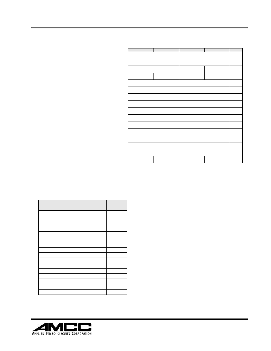
S5933 Architecture
The block diagram in figure 1 above shows the
major functional elements within the S5933. The
S5933 provides three physical bus interfaces: the
PCI Local bus, the user local bus referred to as the
Add-On Local bus and the optional serial and byte-
wide non-volatile memory buses. Data movement
between buses can take place through mailbox reg-
isters or the FIFO data channel, or a user can define
and enable one or more of the four Pass-Thru data
channels. S5933 Bus Master or DMA data transfers
to and from the PCI Local bus are performed
through the FIFO data channel under either Host or
Add-On software control or Add-On hardware con-
trol using dedicated S5933 signal pins.
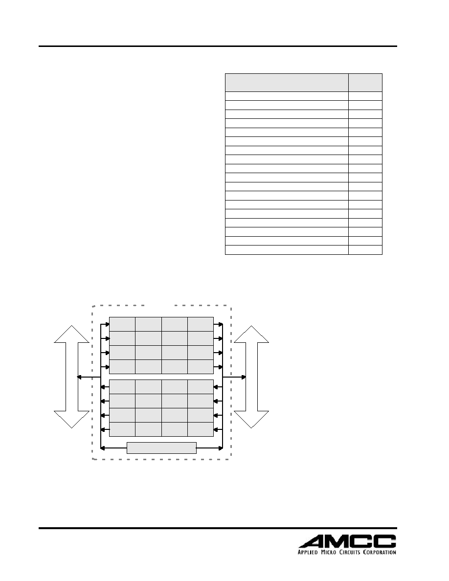
The S5933 signal pins are shown in Figure 2 right.
The PCI Local Bus signals are detailed on the left
side; Add-On Local Bus signal are detailed on the
right side. All additional S5933 device control sig-
nals are shown on the lower right side.
The S5933 supports a two wire serial nvRAM bus
and a byte-wide EPROM/FLASH bus. This allows
the designer to customize the S5933 configuration
by loading setup information on system power-up.
S5933 Register Architecture
Control and configuration of the Add-On Local bus, and the MatchMaker itself, is performed through three primary
groups of registers. These groups consist of PCI Configuration Registers, PCI Operation Registers and Add-On Oper-
ation Registers. All these registers are user configurable through their associated bus or from an external non-volatile
memory device. This section will provide a brief overview of each of these register groups and the optional non-vola-
tile interface.
Add-On Bus
Control
S5933 Register
Access
Pass-Thru
Control/Access
Serial Bus
Config/BIOS Opt.
PCI
Local
Bus
S5933
Control
Add-On
Data Bus
Direct FIFO
Access
Byte Wide
Config/BIOS Opt.
BPCLK
RDFIFO#
SYSRST#
IRQ#
WRFIFO#
DQ[31:0]
SELECT#
ADR[6:2]
BE[3:0]#
RD#
WR#
PTATN#
PTBURST#
PTNUM[1:0]#
PTBE[3:0]#
PTADR#
PTWR
PTRDY#
RDEMPTY
WRFULL
EA[15:0]
EQ[7:0]
EWR#/SDA
ERD#/SCL
PCLK
INTA#
RST#
AD[31:0]
C/BE[3:0]#
FRAME#
DEVSEL#
IRDY#
TRDY#
IDSEL#
STOP#
LOCK#
PAR
PERR#
SERR#
FLT#
S5933
GNT#
REQ#
MODE
SNV
Figure 2
Figure 1
6290 Sequence Drive, San Diego, California 92121-4358 800-755-2622
3
S5933
32-Bit PCI "MatchMaker"
Device ID
PCI Status
Class Code
Base Address Register 0
Base Address Register 2
Base Address Register 4
Reserved Space
Expansion ROM Base Address
Reserved Space
Built-In Self Test
Header Type
Reserved Space
Max. Latency
Min. Grant
Vendor ID
PCI Command
Revision ID
Base Address Register 1
Base Address Register 3
Base Address Register 5
CacheLine Size
Latency Timer
Interrupt Line
Interrupt Pin
Byte 3
Byte 2
Byte 0
Byte 1
Address
00h
04h
08h
0Ch
10h
14h
18h
1Ch
20h
24h
28h
2Ch
30h
34h
38h
3Ch
Reserved Space
PCI Configuration Registers
All PCI compliant devices are required to pro-
vide a group of Configuration Registers for the
host system. These registers are polled during
power up initialization and contain specific
device and add-in card product information
including Vendor ID, Device ID, Revision and
the amount of memory required for product
operation. The S5933 can either load these reg-
isters with default values or initialize them from
an external non-volatile memory area called
'Configuration Space'. The S5933 can accom-
modate a total of 256 bytes of external memory
for this purpose. The first 64 bytes is reserved
for user defined configuration data which is
loaded into the PCI Configuration Registers
during power-up initialization. The remaining
192 bytes may be used to implement an Expan-
sion BIOS or contain add-in card POST code.
Table 1 shows all the S5933 PCI Configuration
Registers.
PCI Operation Registers
The second group of registers are the PCI Oper-
ation Registers shown in Table 2. This group
consists of sixteen 32-bit (DWORD) registers
accessible to the Host processor from the PCI Local bus. These are the main registers through which the PCI Host
configures S5933 operation and communicates with the Add-On Local bus. These registers encompass the PCI bus
incoming and outgoing Mailboxes, FIFO data channel, Bus
Master Address and Count registers, Pass-Thru data channel
registers and S5933 device Status and Control registers.
Add-On Bus Operation Registers
The third and last register group consists of the Add-On
Operation Registers, shown in Table 3. This group of eigh-
teen 32-bit (DWORD) registers is accessible to the Add-On
Local bus. These are the main registers through which the
Add-On logic configures S5933 operation and communicates
with the PCI Local bus. These registers encompass the Add-
On bus Mailboxes, Add-On FIFO, DMA Address/Count Reg-
isters (when Add-On initiated Bus Mastering), Pass-Thru
Registers and Status/Control registers.
Non-Volatile Memory Interface
The S5933 contains a set of PCI Configuration Registers.
These registers can be initialized with default values or with
designer specified values contained in an external nvRAM.
The nvRAM can be either a serial (2 Kbytes, maximum) or a
byte-wide device (64 Kbytes, maximum).
PCI Operation Registers
Outgoing Mailbox Register 1 (OMB1)
Incoming Mailbox Register 1 (IMB1)
Mailbox Empty/Full Status Register (MBEF)
Interrupt Control/Status Register (INTCSR)
Bus Master Control/Status Register (MCSR)
Address
Offset
00h
10h
34h
38h
3Ch
Outgoing Mailbox Register 2 (OMB2)
04h
Outgoing Mailbox Register 3 (OMB3)
08h
Outgoing Mailbox Register 4 (OMB4)
0Ch
Incoming Mailbox Register 2 (IMB2)
14h
Incoming Mailbox Register 3 (IMB3)
18h
Incoming Mailbox Register 4 (IMB4)
1Ch
FIFO Register Port (bidirectional) (FIFO)
20h
Master Write Address Register (MWAR)
24h
Master Write Transfer Count Register (MWTC)
28h
Master Read Address Register (MRAR)
2Ch
Master Read Transfer Count Register (MRTC)
30h
Table 2
Table 1
6290 Sequence Drive, San Diego, California 92121-4358 800-755-2622
4
S5933
32-Bit PCI "MatchMaker"
Add-On Bus Operation Registers
Incoming Mailbox Register 1 (AIMB1)
Outgoing Mailbox Register 1 (AOMB1)
Pass-Thru Address Register (APTA)
Pass-Thru Data Register (APTD)
Maibox Empty/Full Status Register (AMBEF)
Interrupt Control/Status Register (AINT)
General Control/Status Register (ARCR)
Bus Master Write Transfer Count (MWTC)
Address
00h
10h
28h
2Ch
34h
38h
3Ch
58h
Incoming Mailbox Register 2 (AIMB2)
04h
Incoming Mailbox Register 3 (AIMB3)
08h
Incoming Mailbox Register 4 (AIMB4)
0Ch
Outgoing Mailbox Register 2 (AOMB2)
14h
Outgoing Mailbox Register 3 (AOMB3)
18h
Outgoing Mailbox Register 4 (AOMB4)
1Ch
FIFO Port (AFIFO)
20h
Bus Master Write Address Register (MWAR)
24h
Bus Master Read Address Register (MRAR)
30h
Bus Master Read Transfer Count (MRTC)
5Ch
The optional nvRAM allows the Add-On card manufac-
turer to initialize the S5933 with his specific Vendor ID
and Device ID numbers along with desired S5933 opera-
tion characteristics. The non-volatile memory feature
also provides for the Expansion BIOS and POST code
(power-on-self-test) options on the PCI bus.
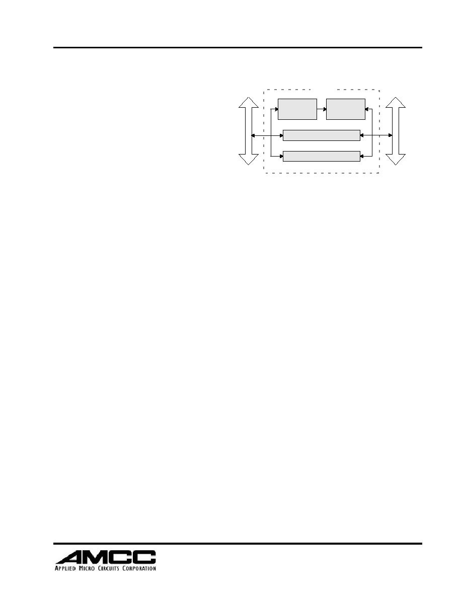
Mailbox Operation
The Mailbox Registers are divided into two four
DWORD sets. Each set is dedicated to one bus for trans-
ferring data to the other bus. Figure 3 below shows a
block diagram of the mailbox section of the S5933. The
provision of Mailbox Registers provides an easy path for
the transfer of user information (command, status or
parametric data) between the two buses. An empty/full
indication for each Mailbox Register, at the byte level, is
determined by polling a Status Register accessible to
both the PCI and Add-On buses. Providing Mailbox byte
level empty/full indications allows for greater flexibility
in 8-, 16- or 32-bit system interfaces. i.e., transferring a
single byte to an 8-bit Add-On bus without requiring the
assembling or disassembling of 32-bit data.
The generation of interrupts from Mailbox Registers is
equivalent with the commonly known 'DOORBELL'
interrupt technique. Bit locations
configured within the S5933's Oper-
ation Registers select a Mailbox and
Mailbox byte which is to generate an
interrupt when full or touched. A
mailbox interrupt control register is
then used to enable interrupt genera-
tion and to select if the interrupt is to
be generated on the PCI or Add-On
Local bus. PCI Local bus interrupts
may also be generated from direct
hardware interfacing due to a unique
AMCC feature. A dedicated Mail-
box byte of the S5933 is directly
accessible via a set of hardware
device signal pins. A single mailbox
load signal pin latches Add-On bus
data directly into the Mailbox initiat-
ing a PCI bus interrupt if enabled.
The mailbox data may also be read
in a similar manner. This option is
shared with the byte wide non-vola-
tile memory signal pins. The S5933
must use the serial nvRAM option for the direct mailbox option signals to be available or they will be assigned to the
byte wide at power up.
Table 3
P
C
I
L
o
c
a
l
B
u
s
Mailbox Status Register
S5933
A
d
d
-
O
n
L
o
c
a
l
B
u
s
PCI MB1
Byte 0
PCI MB2
Byte 0
PCI MB3
Byte 0
PCI MB4
Byte 0
PCI MB1
Byte 1
PCI MB2
Byte 1
PCI MB3
Byte 1
PCI MB4
Byte 1
PCI MB1
Byte 2
PCI MB2
Byte 2
PCI MB3
Byte 2
PCI MB4
Byte 2
PCI MB1
Byte 3
PCI MB2
Byte 3
PCI MB3
Byte 3
PCI MB4
Byte 3
Add MB1
Byte 0
Add MB2
Byte 0
Add MB3
Byte 0
Add MB4
Byte 0
Add MB1
Byte 1
Add MB2
Byte 1
Add MB3
Byte 1
Add MB4
Byte 1
Add MB1
Byte 2
Add MB2
Byte 2
Add MB3
Byte 2
Add MB4
Byte 2
Add MB1
Byte 3
Add MB2
Byte 3
Add MB3
Byte 3
Add MB4
Byte 3
Figure 3
6290 Sequence Drive, San Diego, California 92121-4358 800-755-2622
5
S5933
32-Bit PCI "MatchMaker"
Pass-Thru Operation
Pass-Thru operation executes PCI bus cycles in real
time with the Add-On bus. This allows the PCI bus
to directly read or write to Add-On resources. The
S5933 allows the designer to declare up to four indi-
vidual Pass-Thru Regions. Each region may be
defined as 8-, 16-, or 32-bits wide, mapped into host
memory or I/O space and may be up to 512MB bytes
in size. Figure 4 right shows a block diagram of the
S5933 Pass-Thru architecture.
Pass-Thru operations are performed in PCI target
only mode, making this data channel useful for con-
verting existing ISA or EISA designs over to the fast
PCI architecture. The Pass-Thru data channel uti-
lizes separate Add-On bus signal pins to reflect a
PCI bus read or write request. Add-On logic decodes these signals to determine if it must read or write data to the
S5933 to satisfy the request. Information decoded includes PCI request occurring, the byte lanes involved, the spe-
cific Pass-Thru region accessed and if the request is a burst or single-cycle access. All requested Pass-Thru address
and data information is passed via Add-On Operation Registers.
Pass-Thru operation supports single PCI data cycles and PCI data bursts. During PCI burst operations, the S5933 is
capable of transferring data at the full PCI bandwidth. Should slower Add-On logic be implemented, the S5933 auto-
matically issues PCI bus waits or a Host retry indication until the requested transfer is satisfied.
FIFO PCI Bus Mastering Operation
FIFO PCI Bus Master data transfers are processed by one of two 8-DWORD FIFOs. The FIFO block diagram is
shown in Figure 5. The particular FIFO selected for a data transfer is dependent only on the direction of data flow and
is completely transparent to the user. Internal S5933 decode logic selects the FIFO that is dedicated to transferring
data to the other bus.
The way data is transferred by a FIFO, is determined by Operation and Configuration Registers contained within the
S5933. A FIFO may be configured for either PCI or Add-On initiated Bus Mastering with programmable byte
advance conditions, read vs. write priorities and Add-On bus widths. Advance conditions allow the FIFO to imple-
ment 8-, 16- or 32-bit bus widths. Configuring the S5933 for Bus Master operation enables separate address and data
count registers, which are loaded with the PCI memory address location and number of bytes to be read or written.
This is accomplished by either the Host CPU or Add-On logic. Data can be transferred between the two buses trans-
parent to the PCI Host processor, however, the Add-On logic is required to service the S5933 Add-On Local bus. An
indication of transfer completion can be seen by polling a status register done bit or S5933 signal pin or enabling a
'transfer count = 0' interrupt to either bus.
Further FIFO configuration bits select 16, 32, or 64 bit Endian conversion options for incoming and outgoing data.
Endian conversion allows an Add-On processor and the host to transfer data in their native Endian format. Other con-
figuration bits determine if the Add-On Local bus width is 8, 16 or 32 bits. 16-bit bus configurations internally steer
FIFO data from the upper 16 bits of the DWORD and then to the lower 16-bits on alternate accesses. FIFO pointers
are then updated when appropriate bytes are accessed. Other methods are available for 8-bit or 16-bit Add-Ons.
Efficient FIFO management configuration schemes unique to the AMCC S5933 specify how full or empty a FIFO
must be before it requests the PCI Local bus. These criteria include bus requests when any of the 8 DWORDs are
empty, or when four or more DWORDs are empty. This allows the designer to control how often the S5933 requests
the bus. The S5933 always attempts to perform burst operations to empty or fill the FIFOs. Further FIFO capabilities
over the standard register access methods allow for direct hardware FIFO access. This is provided through separate
access pins on the S5933. Other status output pins allow for easily cascading external FIFOs to the Add-On design.
P
C
I
L
o
c
a
l
B
u
s
S5933
Add-On Pass-Thru Read Data
Add-On Pass-Thru Write Data
A
d
d
-
O
n
L
o
c
a
l
B
u
s
Address Latch
Add-On Pass-
Thru Address
Register
Figure 4