 | –≠–ª–µ–∫—Ç—Ä–æ–Ω–Ω—ã–π –∫–æ–º–ø–æ–Ω–µ–Ω—Ç: S6003 | –°–∫–∞—á–∞—Ç—å:  PDF PDF  ZIP ZIP |
Applied Micro Circuits Corporation
6195 Lusk Blvd., San Diego, CA 92121 ∑ (619) 450-9333
S3005/S3006 EVALUATION BOARD
S6004
Page 1
August 4, 1994
BiCMOS PECL CLOCK GENERATOR
EVALUATION BOARD
Æ
S3005/S3006 EVALUATION BOARD
S6004
VEE
VCC
LEDVCC
REFCLKP
DLDP
DLDP
REFCLKN
TSDP
RSDP
TSDN
LLCLKP
RSDN
LLCLKP
LLCLKN
LLDP
LLCLKN
JP8
JP7
LLDN
S3
S1
RESET
S2
S3006
S3005
D1
U2
1
0
1
0
U1
S3005
XTAL
S3006
XTAL
GND
GND
LEDGND
DLDN
DLDN
LLDP
LLDN
REFCLKN
REFCLKP
TSCLKP
TSCLKN
H1
H4
H2
JP10
JP9
≠2V
JP6
JP5
JP4
JP3
JP1
2
4
6
8
10
12
14
16
18
20
22
24
26
28
30
32
34
36
38
40
42
44
46
48
50
52
54
56
58
60
1
3
5
7
9
11
13
15
17
19
21
23
25
27
29
31
33
35
37
39
41
43
45
47
49
51
53
55
57
59
H3
2
4
6
8
10
12
14
16
18
20
22
24
26
28
30
32
34
36
38
40
42
44
46
48
50
52
54
56
58
60
1
3
5
7
9
11
13
15
17
19
21
23
25
27
29
31
33
35
37
39
41
43
45
47
49
51
53
55
57
59
JP2
JPB
JPA
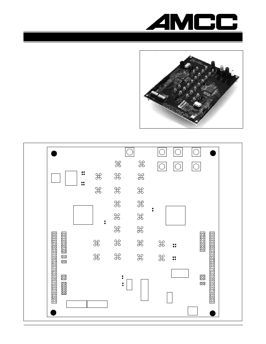
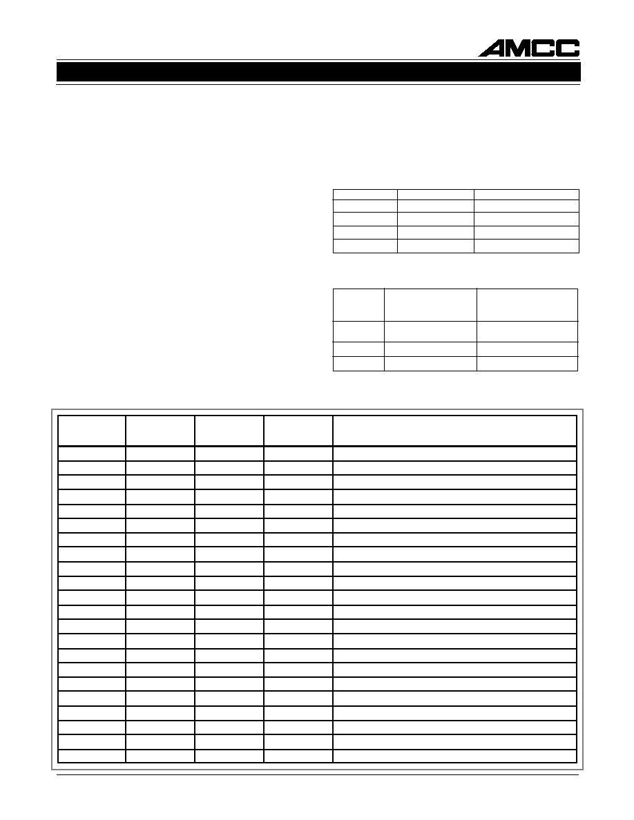
Figure 1. Board Layout
EVALUATION BOARD DESCRIPTION
The S6004 SONET Evaluation Board allows dem-
onstration of AMCC's S3005 and S3006 SONET/
SDH OC-3/12 transmitter/receiver chipset. This data
sheet provides information on board contents and
layout. It should be used in conjunction with the
S3005/S3006 data sheets, which contain full techni-
cal details on chip operation.
Figure 1 depicts the layout of the evaluation board,
showing the location of connectors and components.
Power is supplied to the board from external sup-
plies connected through the on-board banana jacks.
Connectors allow easy access to all of the interface
signals on the S3005/S3006 chips.
Applied Micro Circuits Corporation
6195 Lusk Blvd., San Diego, CA 92121 ∑ (619) 450-9333
Page 2
S6004
S3005/S3006 EVALUATION BOARD
August 4, 1994
ELECTRICAL CONNECTIONS
The 60-pin header strips H1 and H3 allow simple
ribbon cable connections to and from a user-pro-
vided pattern generator. Parallel data can be input to
the S3005 transmitter either through the connector
pins, or by using DIP switch S1. The on-board LED
bank provides checks on output signals. DIP
switches S1, S2, and S3 allow access to the control
signals of both the S3005 and S3006 chips.
Banana jacks are provided for the power connec-
tions. Coaxial SMA connectors are used for serial
data link and external reference clock connections.
Pin Names
Pin No. Level
I/O
Description
GND
31
-
-
Ground
PCLK
32 TTL/CMOS
O
Parallel Clock
GND
33
-
-
Ground
GND
34
-
-
Ground
GND
35
-
-
Ground
LOCKDET
36
TTL
O
Lock Detect
GND
37
-
-
Ground
PIN0
38
TTL
I
Parallel data input
GND
39
-
-
Ground
PIN1
40
TTL
I
Parallel data input
GND
41
-
-
Ground
GND
42
-
-
Ground
GND
43
-
-
Ground
PIN2
44
TTL
I
Parallel data input
GND
45
-
-
Ground
PIN3
46
TTL
I
Parallel data input
GND
47
-
-
Ground
PIN4
48
TTL
I
Parallel data input
GND
49
-
-
Ground
PIN5
50
TTL
I
Parallel data input
GND
51
-
-
Ground
PIN6
52
TTL
I
Parallel data input
GND
53
-
-
Ground
PIN7
54
TTL
I
Parallel data input
GND
55
-
-
Ground
GND
56
-
-
Ground
GND
57
-
-
Ground
GND
58
-
-
Ground
GND
59
-
-
Ground
GND
60
-
-
Ground
Pin Names
Pin No.
Level
I/O
Description
GND
1
-
-
Ground
SYNC
2
TTL
I
Synchronization Enable
GND
3
-
-
Ground
REFSEL1
4
TTL
I
Reference Select 1
GND
5
-
-
Ground
REFSEL0
6
TTL
I
Reference Select 0
GND
7
-
-
Ground
MODE2
8
TTL
I
Mode Select 2
GND
9
-
-
Ground
MODE1
10
TTL
I
Mode Select 1
GND
11
-
-
Ground
MODE0
12
TTL
I
Mode Select 0
GND
13
-
-
Ground
DLCV
14
TTL
I
Diag. Line Code Violation
GND
15
-
-
Ground
DLEB
16
TTL
I
Diag. Loopback Enable
GND
17
-
-
Ground
LLEB
18
TTL
I
Line Loopback Enable
GND
19
-
-
Ground
Table 2. H1 Pin Descriptions
PAE
20 TTL/CMOS
O
Phase Alignment Event
GND
21
-
-
Ground
RSTB
22
TTL
I
Master Reset
GND
23
-
-
Ground
BYTCLKIP
24 TTL/CMOS
O
Reference Feedback Clock
GND
25
-
-
Ground
TESTEN
26
TTL
I
Test Clock Enable
GND
27
-
-
Ground
PICLK
28
TTL
I
Parallel Input Clock
GND
29
-
-
Ground
GND
30
≠
≠
Ground
Refer to Figure 1 for locations of the connectors dis-
cussed in the following sections. All connectors, con-
trols, and jumpers are labeled on the board.
Power Connections
Power connections are made through the on-board
banana jacks (VCC, VEE, GND, LEDVCC, and
LEDGND). Refer to Table 1 for recommended oper-
ating conditions. A ≠2V connection provides proper
on-board termination for the DLDP/N outputs of
the S3005 when connected to the DLDP/N inputs
of the S3006.
Table 1. Power Connection
Recommended Operating Conditions
Power Supply
Nominal Input Voltage
VCC
5 V
Ground
0 V
VEE
-4.5 or -5.2V
LEDVCC
5 V
Applied Micro Circuits Corporation
6195 Lusk Blvd., San Diego, CA 92121 ∑ (619) 450-9333
S3005/S3006 EVALUATION BOARD
S6004
Page 3
August 4, 1994
Pin Names
Pin No.
Level
I/O
Description
SYNC
1
TTL
Input
SYNC input (pin 58) of S3005
SYNC
2
TTL
Input
DIP Switch S2 position 9
REFSEL1
3
TTL
Input
REFSEL1 input (pin 28) of S3005
REFSEL1
4
TTL
Input
DIP Switch S2 position 8
REFSEL0
5
TTL
Input
REFSEL0 input (pin 27) of S3005
REFSEL0
6
TTL
Input
DIP Switch S2 position 7
MODE2
7
TTL
Input
MODE2 input (pin 66) of S3005
MODE2
8
TTL
Input
DIP Switch S2 position 6
MODE1
9
TTL
Input
MODE1 input (pin 63) of S3005 and (pin 28) of S3006
MODE1
10
TTL
Input
DIP Switch S2 position 5
MODE0
11
TTL
Input
MODE0 input (pin 65) of S3005 and (pin 29) of S3006
MODE0
12
TTL
Input
DIP Switch S2 position 4
DLCV
13
TTL
Input
DLCV input (pin 59) of S3005
DLCV
14
TTL
Input
DIP Switch S2 position 3
DLEB
15
TTL
Input
DLEB input (pin 26) of S3005 and (pin 57) of S3006
DLEB
16
TTL
Input
DIP Switch S2 position 2
LLEB
17
TTL
Input
LLEB input (pin 57) of S3005
LLEB
18
TTL
Input
DIP Switch S2 position 1
RSTB
19
TTL
Input
RSTB input (pin 29) of S3005 and (pin 21) of S3006
RSTB
20
TTL
Input
RESET switch
TESTEN
21
TTL
Input
TESTEN input (pin 31) of S3005
TESTEN
22
TTL
Input
DIP Switch S1 position 9
PIN0
23
TTL
Input
PIN0 input (pin 14) of S3005
PIN0
24
TTL
Input
DIP Switch S1 position 8
PIN1
25
TTL
Input
PIN1 input (pin 12) of S3005
PIN1
26
TTL
Input
DIP Switch S1 position 7
PIN2
27
TTL
Input
PIN2 input (pin 10) of S3005
PIN2
28
TTL
Input
DIP Switch S1 position 6
PIN3
29
TTL
Input
PIN3 input (pin 9) of S3005
PIN3
30
TTL
Input
DIP Switch S1 position 5
PIN4
31
TTL
Input
PIN4 input (pin 8) of S3005
PIN4
32
TTL
Input
DIP Switch S1 position 4
PIN5
33
TTL
Input
PIN5 input (pin 5) of S3005
PIN5
34
TTL
Input
DIP Switch S1 position 3
PIN6
35
TTL
Input
PIN6 input (pin 3) of S3005
PIN6
36
TTL
Input
DIP Switch S1 position 2
PIN7
37
TTL
Input
PIN7 input (pin 2) of S3005
PIN7
38
TTL
Input
DIP Switch S1 position 1
Transmitter Signals--Headers H1 and H2
Header H1 allows connection to a 60-pin ribbon
cable or to single discrete cables. Controls for sig-
nals RSTB, DLEB, MODE0, and MODE1 are com-
mon to both transmitter and receiver and can be
controlled via header H1. These signals can also be
controlled by dipswitch S2 if H2 jumpers are installed.
Header H2 allows for DIP SWITCH control of signals
SYNC, REFSEL [1:0], MODE [2:0], DLCV, DLEB,
LLEB, TESTEN, and PIN[7:0]. Control of each sig-
nal will be transferred to the corresponding DIP
switch SI or S2 when the corresponding jumpers are
installed on H2. (See Table 3.)
Table 3. H2 Pin Descriptions
Applied Micro Circuits Corporation
6195 Lusk Blvd., San Diego, CA 92121 ∑ (619) 450-9333
Page 4
S6004
S3005/S3006 EVALUATION BOARD
August 4, 1994
Receiver Signals--Headers H3 and H4
Header H3 allows connection to a 60-pin ribbon
cable or to single discrete cables. (Controls for sig-
nals RSTB, DLEB, MODE0, and MODE1 are com-
mon to both the transmitter and receiver and can be
controlled via header H1. These signals can also be
controlled by dipswitch S2 if H2 jumpers are in-
stalled. Mode2 is controlled via header H3. If the
Mode2 jumper is installed, the Mode2 input will be
low. If the Mode2 jumper is not installed, the Mode2
input will float to a high state.) When the associated
pins on header H4 are jumpered, signals REFSEL
[1:0] and TESTRST will be connected to DIP
SWITCH S3. (See Table 3.) Without using any
jumpers on these signal pins, they can be accessed
directly by a 60-pin ribbon cable attached to header
H3. Signal pins POUT [7:0] are always tied to LED
bank D1, and can also be accessed by the same 60-
pin ribbon cable by jumpering those outputs on
header H4. Refer to Table 4 for pin descriptions of
Header H3.
Pin Names
Pin No. Level
I/O
Description
GND
31
-
-
Ground
POCLK
32 TTL/CMOS
O
Parallel Output Clock
GND
33
-
-
Ground
GND
34
-
-
Ground
GND
35
-
-
Ground
TESTEN
36
TTL
I
Test Clock Enable
GND
37
-
-
Ground
REFSEL1
38
TTL
I
Reference Select 1
GND
39
-
-
Ground
REFSEL0
40
TTL
I
Reference Select 0
GND
41
-
-
Ground
GND
42
-
-
Ground
GND
43
-
-
Ground
TESTRST
44
TTL
I
Test Reset
GND
45
-
-
Ground
LCV
46 TTL/CMOS
O
Line Code Violation
GND
47
-
-
Ground
FP
48 TTL/CMOS
O
Frame Pulse
GND
49
-
-
Ground
-
50
-
-
-
GND
51
-
-
Ground
-
52
-
-
-
GND
53
-
-
Ground
-
54
-
-
-
GND
55
-
-
Ground
GND
56
-
-
Ground
GND
57
-
-
Ground
GND
58
-
-
Ground
GND
59
-
-
Ground
GND
60
-
-
Ground
Table 4. H3 Pin Description
Pin Names
Pin No.
Level
I/O
Description
GND
1
-
-
Ground
POUT0
2 TTL/CMOS
O
Parallel data output
GND
3
-
-
Ground
POUT1
4 TTL/CMOS
O
Parallel data output
GND
5
-
-
Ground
POUT2
6 TTL/CMOS
O
Parallel data output
GND
7
-
-
Ground
POUT3
8 TTL/CMOS
O
Parallel data output
GND
9
-
-
Ground
POUT4
10 TTL/CMOS
O
Parallel data output
GND
11
-
-
Ground
POUT5
12 TTL/CMOS
O
Parallel data output
GND
13
-
-
Ground
POUT6
14 TTL/CMOS
O
Parallel data output
GND
15
-
-
Ground
POUT7
16 TTL/CMOS
O
Parallel data output
GND
17
-
-
Ground
LOCKDET
18
TTL
O
Lock Detect
GND
19
-
-
Ground
OOF
20
TTL
I
Out of Frame
GND
21
-
-
Ground
LOS
22
ECL
I
Loss of Signal
GND
23
-
-
Ground
MODE2
24
TTL
I
Operating Mode
GND
25
-
-
Ground
-
26
-
-
-
GND
27
-
-
Ground
BYTCLKIP
28 TTL/CMOS
O
Ref. Feedback Clock
GND
29
-
-
Ground
GND
30
-
-
Ground
RESET
When the RSTB pins on Header H2 are shorted to
each other, the push button switch on the top left of
the board is connected to the S3005 and S3006
RSTB Master Reset inputs.
CRYSTAL REFERENCES AND CLOCK
GENERATION
Two 19.44-MHz differential ECL crystal oscillators
with 100-ppm stability are provided, one each for the
transmitter and receiver. If a higher reference fre-
quency is needed (38.88, 51.84, or 77.76 MHz), it
can be selected by setting the two reference select
input pins. The correct frequency is set with the
REFSEL[1:0] inputs as shown in Table 6.
The output clock frequency can be 155.52 MHz
(STS-3), 311.04 MHz (STS-3 CMI), or 622.08 MHz
(STS-12). The output frequency is set with the
MODE[2:0] inputs as shown in Table 7.
Applied Micro Circuits Corporation
6195 Lusk Blvd., San Diego, CA 92121 ∑ (619) 450-9333
S3005/S3006 EVALUATION BOARD
S6004
Page 5
August 4, 1994
To use the S3005 crystal oscillator as its reference,
install jumpers on JP8 and JP10. To use an external
reference clock through the S3005 REFCLKP/N
SMA connector, install jumpers on JP7 and JP9. To
use the S3006 crystal oscillator as its reference, in-
stall jumpers on JP3 and JP5. To use an external
reference clock through the S3006 REFCLKP/N
SMA connector, install jumpers on JP4 and JP6.
(See Table 9, Jumpers.)
LEDs
The bank of 10 LEDs (D1) display when the S3005/
S3006 chips are locked, and also light when the ap-
propriate POUT is in the high state. The function of
each LED is shown in Table 8, and is also labeled
on the board.
SMA Connectors
SMA connectors provide input/output capability for a
number of signals, including serial data I/O and ref-
erence clocks. These connectors are labeled on the
board and are also shown in Figure 1.
Table 5. H4 Pin Description
Pin
Names
Pin No.
Level
I/O
Description
POUT0
1
TTL/CMOS
Output
POUT0 output (pin 14) of S3006
POUT0
2
TTL/CMOS
Output
Connected to H3 pin 2
POUT1
3
TTL/CMOS
Output
POUT1 output (pin 12) of S3006
POUT1
4
TTL/CMOS
Output
Connected to H3 pin 4
POUT2
5
TTL/CMOS
Output
POUT2 output (pin 10) of S3006
POUT2
6
TTL/CMOS
Output
Connected to H3 pin 6
POUT3
7
TTL/CMOS
Output
POUT3 output (pin 9) of S3006
POUT3
8
TTL/CMOS
Output
Connected to H3 pin 8
POUT4
9
TTL/CMOS
Output
POUT4 output (pin 8) of S3006
POUT4
10
TTL/CMOS
Output
Connected to H3 pin 10
POUT5
11
TTL/CMOS
Output
POUT5 output (pin 5) of S3006
POUT5
12
TTL/CMOS
Output
Connected to H3 pin 12
POUT6
13
TTL/CMOS
Output
POUT6 output (pin 3) of S3006
POUT6
14
TTL/CMOS
Output
Connected to H3 pin 14
POUT7
15
TTL/CMOS
Output
POUT7 output (pin 2) of S3006
POUT7
16
TTL/CMOS
Output
Connected to H3 pin 16
REFSEL1
17
TTL
Input
Dip Switch S3 position 1
REFSEL1
18
TTL
Input
Connected to H3 pin 38
REFSEL0
19
TTL
Input
Dip Switch S3 position 2
REFSEL0
20
TTL
Input
Connected to H3 pin 40
TESTRST
21
TTL
Input
Dip Switch S3 position 3
TESTRST
22
TTL
Input
Connected to H3 pin 44
Jumpers
A number of jumpers allow the user to control vari-
ous aspects of the characterization procedure. The
function of each jumper is described in Table 9.
REFSEL1
REFSEL0
FREQUENCY
0
0
19.44 MHz
0
1
38.88 MHz
1
0
51.84 MHz
1
1
77.76 MHz
Table 6. REFSEL Settings
FREQ.
BYPASS MODE
NORMAL MODE
(TESTEN = 1)
(TESTEN = 0)
Mode2 Mode1 Mode0 Mode2 Mode1 Mode0
622.08 MHz
1
0
0
1
0
0
311.04 MHz
1
0
1
0
0
1
155.52 MHz
1
1
0
0
1
0
Table 7. Output Clock Frequency Settings