Applied Micro Circuits Corporation
6195 Lusk Blvd., San Diego, CA 92121 ∑ (619) 450-9333
Page 1
October 23, 1995
BiCMOS PECL CLOCK GENERATOR
Æ
PRELIMINARY
EVALUATION MANUAL
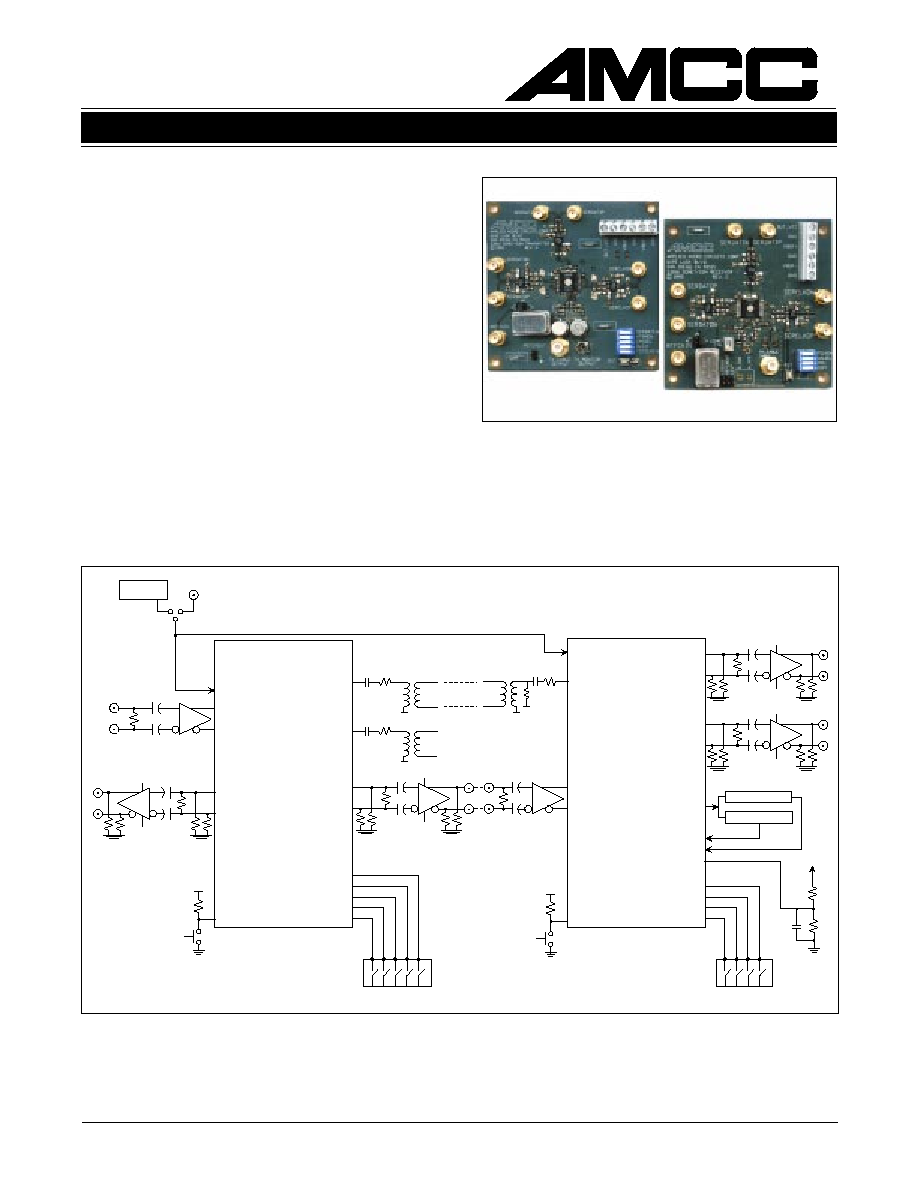
The S6006 Evaluation Manual describes two evalua-
tion boards that allow demonstration of AMCC's
S3015/S3016 E4/STM-1/OC-3 SONET/SDH/ATM in-
terface circuits. This document provides information
on board contents and layout. It should be used in
conjunction with the S3015/S3016 data sheet, which
contains full technical details on chip operation.
Figure 1 depicts a block diagram of circuit functional-
ity. Power is supplied to the boards from external raw
supplies connected through the on-board power con-
nections. Connectors allow easy access to all of the
interface signals on the S3015/S3016 chips. All re-
quired external circuitry, including transformers and
passive components, are provided on the boards.
For additional detail on the interface circuitry or for
applications examples, contact AMCC for the S3015/
S3016 "System Interface Application Note".
Figure 1. Functional Block Diagram
S3015/S3016 EVALUATION BOARD
S6006
S3015
REFCKIN
REFCKIN
SERDATIP
SERDATIN
SERDATIP
SERDATIN
RSTB
CMISEL
XFRMDRVB
XFRMDRVA
SERDATOP
SERDATON
RSTB
REFCKIN
SERCLKON
SERDATOP
SERDATON
BUFOUT
BUFIN
LOSREF
EQUALSEL
LOSOPT
TSTCLKEN
ANDATIN
LOSIN
Crystal
Oscillator
S3016
GND
75
Cable
Cable
Output
(BNC)
GND
Monitor
Output
(BNC)
SERDATEN
GND
Cable
Input
(BNC)
LOSIN Compensator
Equalizer
VCC
SERCLKOP
SERCLKON
SERCLKOP
XFRMEN
DLCV
TSTCLKEN
CMISEL
DCTB
DCTB
CVTB
VBUF+
VBUF≠
CVTB
VBUF+
VBUF≠
CVTB
VBUF+
VBUF≠
CVTB
VBUF+
VBUF≠
VCC
Push
Button
Switch
VCC
Push
Button
Switch
Dip Switches
Dip Switches
DCTB = DUT Controlled Termination Buffer
CVTB = Controllable Voltage Termination Buffer
Applied Micro Circuits Corporation
6195 Lusk Blvd., San Diego, CA 92121 ∑ (619) 450-9333
Page 2
October 23, 1995
Table 1. Power Connection
Recommended Operating Conditions
ELECTRICAL CONNECTIONS
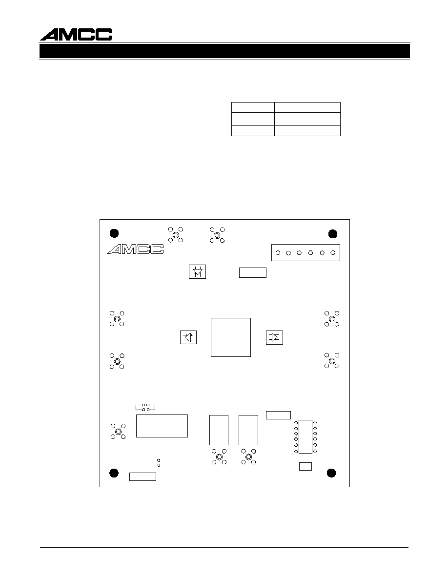
Separate boards are provided for the S3015 and
the S3016 chips. Layouts for both boards are de-
picted in Figures 2 and 3, showing the location of
connectors and components. The various connec-
tions are described in the following sections.
Power Connections
Connections are provided on the board for ground
and VCC. Refer to Table 1 for recommended oper-
ating conditions.
Power Supply Nominal Input Voltage
VCC
5 V
Ground
0 V
S3015/S3016 EVALUATION BOARD
S6006
RST
GND
SERDATEN
XFRMEN
CMISEL
DLCV
TSTCLKEN
SERDATIP
REFCKIN
SERDATIN
A
GND
DUT_VCC
GND
VBUF+
GND
VBUF≠
GND
XFORMER
XFORMER
B
JP1
DIPSWITCH
REFCKOUT
TX_CABLE
OUTPUT
TX_MONITOR
OUTPUT
GND
S3015A
SERCLKOP
SERCLKON
SERDATOP
SERDATON
BUFFER
BUFFER
BUFFER
XTAL
Figure 2. S3015 Board Layout
Applied Micro Circuits Corporation
6195 Lusk Blvd., San Diego, CA 92121 ∑ (619) 450-9333
Page 3
October 23, 1995
Cable Connections - Transmitter
Two BNC connectors allow connection to the follow-
ing two output signals. (See Figure 2 for locations.)
TX_CABLE_OUTPUT. Transformer Output. Drives the
G.703 specified 75
cable. The G.703 output mask
can be measured at this point. A 75
SMB connector
is included for impedance matching and easy inter-
facing to a 75
cable.
TX_MONITOR_OUTPUT. Transformer Output. Drives
the monitor point as specified in G.703. This output is
identical to the TX_OUT signal. A probe socket is
included to allow for easy measurements of trans-
former output.
Cable Connections - Receiver
A BNC connector allows connection to the following
input signal. (See Figure 3 for location.)
RX_CABLE_INPUT. Transformer Input. Receives the
G.703 compliant signal. The G.703 input waveforms
and loss-of-signal detection levels are specified at
this connector. A 75
SMB connector is included for
impedance matching and easy interfacing to a 75
cable.
S3015/S3016 EVALUATION BOARD
S6006
RST
LOSREF
CTRL
S3016A
GND
XTAL
LOSOPT
CMISEL
EQUALSEL
TSTCLKEN
SERDATIP
REFCKIN
SERDATIN
A
SERCLKOP
SERCLKON
SERDATON
EQUALIZER AND
LOSIN COMPENSATOR
CIRCUITRY
SERDATOP
DUT_VCC
GND
VBUF+
GND
VBUF≠
GND
BUFFER
XFORMER
B
JP1
DIPSWITCH
LOSOUT
BUFFER
BUFFER
RX_CABLE
INPUT
REFCKOUT
LCV
Figure 3. S3016 Board Layout
Applied Micro Circuits Corporation
6195 Lusk Blvd., San Diego, CA 92121 ∑ (619) 450-9333
Page 4
October 23, 1995
Overhead Processor Connections - Transmitter
RESET. TTL Input. Initializes the S3015 to a known
logic state.
SERDATIP/N. Differential AC-coupled PECL. SMA
connector that drives the serial data inputs to the CMI
encoder circuit. This input should be supplied with
NRZ data at the appropriate data rate. (See Table 2.)
REFCKIN. TTL input. SMA connector that must be
supplied with the correct reference clock frequency.
(See Table 2.) Used by the S3015 to synthesize the
serial clock.
SERDATOP/N. Differential PECL. This output is the
delayed version of the incoming data stream updated
on the falling edge of SERCLKOP/N.
SERCLKOP/N. Differential PECL. This output is
phase-aligned with SERDATOP/N.
REFCKIN. TTL input. SMA connector that must be
supplied with the correct reference clock frequency.
(See Table 2.) Used by the S3016 to initialize the
receive clock recovery PLL. The reference clock must
be present during reset to guarantee initialization of
the PLL circuits.
SERDATOP/N. Differential AC-coupled PECL output.
SMA connector that drives the decoded CMI data to
the overhead processor.
SERCLKOP/N. Differential PECL. This output is
phase-aligned with SERDATOP/N.
LOSOUT. TTL output. When High, this signal indi-
cates that the clock recovery PLL is detecting valid
data at the serial data inputs and is attempting to lock
to it. When Low, the clock recovery PLL is locked to
REFCKIN.
REFCKOUT. TTL input. Clock output that is at the
same frequency as the REFCKIN input.
DIP Switch - Receiver
An onboard DIP switch provides additional control ca-
pability on the receiver board. The following four sig-
nals are controlled by means of the DIP switch:
LOSOPT. PECL. Active Low. This input is driven by
the external optical receiver module to indicate a loss
of received optical power.
CMISEL. TTL input. A Logic High selects CMI mode;
a Logic Low selects NRZ.
EQUALSEL. TTL input. A Logic High selects
ANDATIN. A Logic Low selects SERDATIP/N.
TSTCLKEN. TTL. Active High. Enables the reference
clock to be used in place of the VCO for testing.
Allows a way to test the chip without the use of the
PLL.
CRYSTAL REFERENCE
A 19.44 MHz or a 17.408 MHz differential ECL crystal
oscillator can be used for the reference clock. One
19.44 MHz crystal is provided on each board. If a
17.408 MHz reference frequency is needed, AMCC
can recommend crystal vendors.
JUMPER CONFIGURATION
The jumpers labeled JP1 on both boards allow the
user to control whether an onboard crystal reference
or external clock reference is used (see Crystal Ref-
erence above). Jumper A is installed when an exter-
nal reference is used, and Jumper B is installed when
the onboard crystal reference is used.
MODE REF CLK FREQ
SERIAL DATA RATE
(REFCKIN/P) MHz (SERDATIP/N, TX_OUT) Mbits/s
STS-3 CMI
19.44
155.52
E4 CMI
17.408
139.264
DIP Switch - Transmitter
An onboard DIP switch provides additional control ca-
pability on the transmitter board. The following five
signals are controlled by means of the DIP switch:
SERDATEN. TTL input. Enables the loopback path
from the S3015 to the S3016. The data from the
SERDATIP/N inputs will be CMI-encoded and sent to
the S3016, where it will be decoded and output on
the SERDATOP/N pins.
XFRMEN. TTL input. Enables the transformer outputs
TX_OUT and MON_OUT.
CMISEL. TTL input. Selects CMI or NRZ. Logic High
selects CMI mode, and Logic Low selects NRZ mode.
DLCV. Singled-ended PECL input. Only active in CMI
mode. Set High to force a CMI line code violation.
TSTCLKEN. TTL input. Enables the reference clock
to be used instead of the VCO for testing, allowing a
means of testing chip functions without the use of the
PLL.
Overhead Processor Connections - Receiver
RESET. TTL Input. Initializes the S3016 to a known
logic state.
SERDATIP/N. Differential PECL. Clock is recovered
from transitions on these inputs.
Table 2. Operating Frequencies
S3015/S3016 EVALUATION BOARD
S6006