
1
HIGH DEFINITION SERIAL DIGITAL INTERFACE (HD-SDI) CHIPSET
S8401/S8501
December 10, 1999 / Revision C
BiCMOS PECL CLOCK GENERATOR
FEATURES
∑ Micro-Power Bipolor technology
∑ SMPTE 292M compliant
∑ 1.485 Gb/s or 1.485/1.001 Gb/s operation
∑ HD-SDI Serializer transmitter incorporates a
Phase Lock Loop (PLL) providing clock synthe-
sis from low-speed reference
∑ HD-SDI Deserializer receiver PLL configured
for clock and data recovery
∑ 20-bit parallel TTL compatible interface
∑ Low-jitter serial PECL compatible interface
∑ Lock detect
∑ Local loopback
∑ Continuous downstream clocking from receiver
∑ Single +3.3V power supply
∑ Compact 52 PQFP package
APPLICATIONS
Parallel to HD-SDI/HD-SDI to parallel interfacing
∑ Compressors
∑ Video graphics
∑ Video editors
∑ Disc storage devices
∑ VTR's
∑ Cameras
∑ Monitors
∑ Frame synchronizers
∑ Character generators
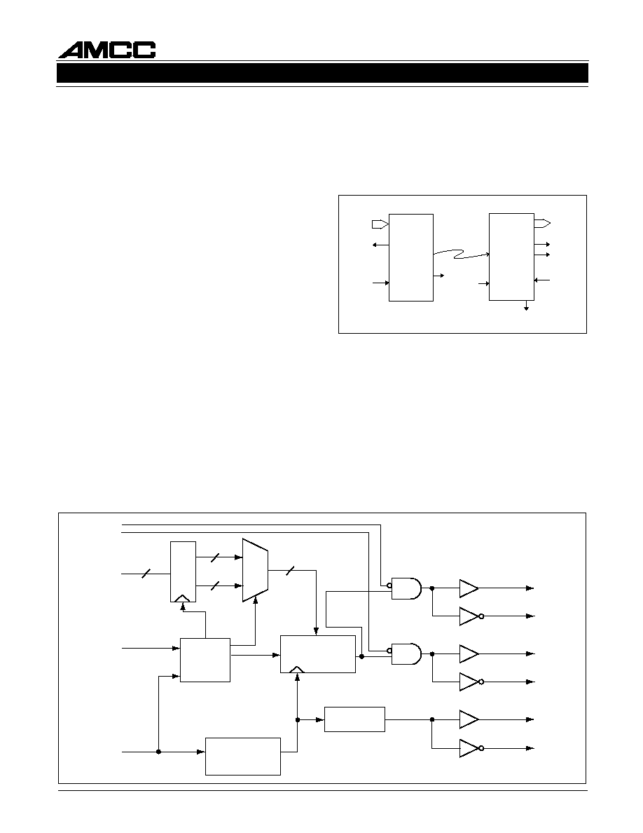
GENERAL DESCRIPTION
The S8401 and S8501 transmitter and receiver pair
are designed to perform HD-SDI over fiber optic or
coaxial cable interfaces conforming to the require-
ments of the SMPTE 292M. The chipset supports
1.485 Gb/s with an associated 20-bit data word.
The chipset performs parallel-to-serial and serial-to-
parallel conversion for scrambled data. The S8401
on-chip PLL synthesizes the high-speed clock from a
low-speed reference. The S8501 on-chip PLL syn-
chronizes directly to incoming digital signals, to receive
the data stream. The transmitter and receiver each
support differential PECL I/O for fiber optic compo-
nent interfaces, to minimize crosstalk and maximize
data integrity. Local loopback allows for system diag-
nostics.
The S8401 and S8501 operate from +3.3V power
supplies. Each chip typically dissipates only 0.70 and
0.90W respectively. Figure 1 shows a typical network
configuration incorporating the chipset.
Figure 1. System Block Diagram
Æ
DEVICE
SPECIFICATION
S8401/S8501
HIGH DEFINITION SERIAL DIGITAL INTERFACE (HD-SDI) CHIPSET
FPGA
Scrambler
S8401
HD-SDI
Serializer
20
DRV
EQ
S8501
HD-SDI
Deserializer
20
FPGA
Descrambler
Framer
Coax
or
Fibre
2
HIGH DEFINITION SERIAL DIGITAL INTERFACE (HD-SDI) CHIPSET
S8401/S8501
December 10, 1999 / Revision C
Loopback
Local loopback is supported by the chipset, and pro-
vides a capability for performing offline testing of the
interface to ensure the integrity of the serial channel
before enabling the transmission medium. It also al-
lows for system diagnostics.
S8401/S8501 OVERVIEW
The S8401 transmitter and S8501 receiver provide
serialization and deserialization functions for
scrambled data to implement a HD-SDI. Operation of
the S8401/S8501 chips is straightforward, as depicted
in Figure 2. The sequence of operations is as follows:
Transmitter
1. 20-bit parallel input
2. Parallel-to-serial conversion
3. Serial output
Receiver
1. Clock and data recovery from serial input
2. Serial-to-parallel conversion
3. 20-bit parallel output
The 20-bit parallel data handled by the S8401 and
S8501 devices should be from a DC-balanced en-
coding scheme, such as the scrambling as defined
by SMPTE-292M.
Internal clocking and control functions are transpar-
ent to the user. Details of data timing can be seen in
Figure 5.
A lock detect feature is provided on the receiver, which
indicates that the PLL is locked (synchronized) to the
data stream.
Figure 2. Interface Diagram
20 Bit
Parallel
Data In
Transmitter
S8401
Receiver
S8501
REFCLK
Lock
Detect
REFCLK
RCLK
Parallel
Data Out
RCLKN
Loopback
Loopback
Serial
Data
TCLK
S8401 TRANSMITTER
Architecture/Functional Description
The S8401 transmitter accepts parallel input data and
serializes it for transmission over fiber optic or coaxial
cable media. The S8401 is compliant with SMPTE
292M Specification, and supports the HD-SDI data
rate of 1.485 Gb/s.
The parallel input data word is 20 bits wide. A block
diagram showing the basic chip function is shown in
Figure 3.
CONTROL
LOGIC
TEST
D[19:0]
OE1
OE0
REFCLK
2:1
10
10
20
10
PLL CLOCK
MULTIPLIER
F0 = F1 X 20
SHIFT
REGISTER
TX
TY
TLX
TLY
TCLK
TCLKN
DIVIDE-BY-20
D
Q
Figure 3. S8401 Functional Block Diagram
3
HIGH DEFINITION SERIAL DIGITAL INTERFACE (HD-SDI) CHIPSET
S8401/S8501
December 10, 1999 / Revision C
Parallel/Serial Conversion
The parallel-to-serial converter takes in 20-bit wide
data from the input latch and converts it to a serial
data stream. Parallel data is latched into the transmit-
ter on the positive going edge of REFCLK. The data
is then clocked synchronous to the clock synthesis
unit serial clock into the serial output shift register.
The shift register is clocked by the internally gener-
ated bit clock which is 20 times the REFCLK input
frequency. The state of the serial outputs is controlled
by the output enable pins, OE0 and OE1. D[0] is
transmitted first.
Reference Clock Input
The reference clock input (REFCLK) must be supplied
with a PECL single-ended AC coupled crystal clock
source with 100 PPM tolerance to assure that the trans-
mitted data meets the SMPTE 292M Specification
frequency limits. The internal serial clock is frequency
locked to the reference clock. Refer to Table 1 for
reference clock frequency.
Table 1. Transmitter Operating Mode
e
t
a
R
a
t
a
D
)
s
p
b
M
(
)
s
p
b
M
(
)
s
p
b
M
(
)
s
p
b
M
(
)
s
p
b
M
(
d
r
o
W
h
t
d
i
W
h
t
d
i
W
h
t
d
i
W
h
t
d
i
W
h
t
d
i
W
)
s
t
i
B
(
)
s
t
i
B
(
)
s
t
i
B
(
)
s
t
i
B
(
)
s
t
i
B
(
e
c
n
e
r
e
f
e
R
k
c
o
l
C
k
c
o
l
C
k
c
o
l
C
k
c
o
l
C
k
c
o
l
C
y
c
n
e
u
q
e
r
F
y
c
n
e
u
q
e
r
F
y
c
n
e
u
q
e
r
F
y
c
n
e
u
q
e
r
F
y
c
n
e
u
q
e
r
F
)
z
H
M
(
)
z
H
M
(
)
z
H
M
(
)
z
H
M
(
)
z
H
M
(
N
K
L
C
T
/
K
L
C
T
y
c
n
e
u
q
e
r
F
y
c
n
e
u
q
e
r
F
y
c
n
e
u
q
e
r
F
y
c
n
e
u
q
e
r
F
y
c
n
e
u
q
e
r
F
)
z
H
M
(
)
z
H
M
(
)
z
H
M
(
)
z
H
M
(
)
z
H
M
(
5
8
4
1
0
2
5
2
.
4
7
5
2
.
4
7
Figure 4. S8501 Functional Block Diagram
PLL CLOCK
RECOVERY
2:1
D
20
D
BITCLK
Q
RX
REFCLK
LOCKREFN
RY
RLX
RLY
LPEN
LOCKDETN
D[19:0]
RCLK
RCLKN
SHIFT
REGISTER
DIVIDER
4
HIGH DEFINITION SERIAL DIGITAL INTERFACE (HD-SDI) CHIPSET
S8401/S8501
December 10, 1999 / Revision C
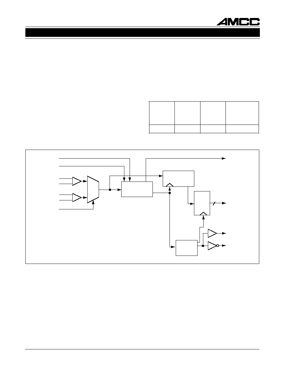
S8501 RECEIVER
Architecture/Functional Description
The S8501 receiver is designed to implement SMPTE
292M Specification receiver functions. A block dia-
gram showing the basic chip function is provided in
Figure 4.
Whenever a signal is present, the S8501 attempts to
achieve bit synchronization of the received encoded
bit stream. Received data from the incoming bit stream
is provided on the device's parallel data outputs.
The S8501 accepts serial encoded data from a fiber
optic or coaxial cable interface. The serial input stream
is the result of the serialization of scrambled data by
a compatible transmitter. Clock recovery is performed
on-chip, with the output data presented to the trans-
mission layer as 20-bit parallel data. The chip operates
at the HD-SDI frequency of 1.485Gb/s.
Serial/Parallel Conversion
Serial data is received on the RX, RY pins. The PLL
clock recovery circuit will lock to the data stream if the
clock to be recovered is within
±
100 PPM of the inter-
nally generated bit rate clock. The recovered clock is
used to retime the input data stream. The data is then
clocked into the serial to parallel output registers.
Reference Clock Input
The reference clock input must be supplied with a
PECL single-ended AC coupled crystal clock source
at
±
100 PPM tolerance. See Table 2 for reference
clock frequency.
Framing
Framing is performed off-chip. Typically, an FPGA
would be used to implement descrambling and Word/
Frame synchronization as required by SMPTE 292M.
Lock Detect
The S8501 lock detect function indicates the state of
the phase-locked loop (PLL) clock recovery unit. The
PLL will indicate lock within 2.5
µ
s after the start of
receiving serial data inputs. If the serial data inputs
have an instantaneous phase jump (from a serial
switch, for example) the PLL will not indicate an out-
of-lock state, but will recover the correct phase
alignment within 250 bit times. If a run length of 80-
160 bits is exceeded the loop will declare loss of lock.
Input data rate variation (compared to REFCLK) can
also cause loss of lock. Table 3 shows the response
of the PLL loop circuit to input data rate variation.
When lock is lost, the PLL will attempt to re-acquire
bit synchronization, and will shift from the serial input
data to the reference clock so that the correct fre-
quency downstream clocking will be maintained.
The LOCKDETN output will go inactive (High) when
no data is present on the serial data inputs. When
LOCKDETN is in the inactive (high) state, it indicates
that the PLL is locking to the local reference clock to
maintain downstream clocking. When LOCKDETN is
in the active (low) state, it indicates that the PLL is
attempting to lock to the incoming serial data. When
serial data is restored, the LOCKDETN output will
stay in the active state.
REFCLK
(Input)
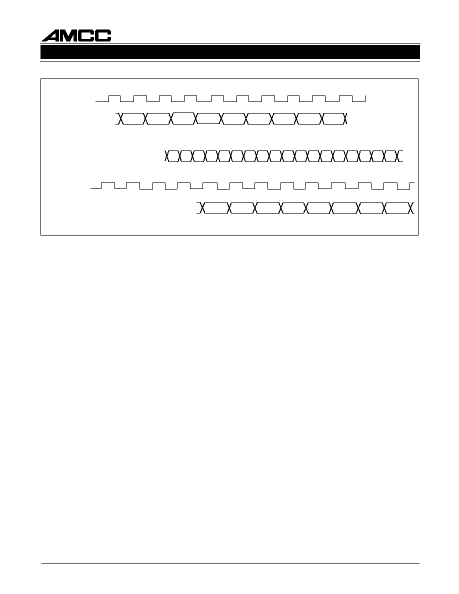
RCLK
(Output)
PARALLEL
DATA BUS
(Input)
D1
D0
D2
D3
D4
D5
D6
D7
D8
D9
D10
D11
D12
D13
D14
D15
PARALLEL
DATA BUS
(Output)
SERIAL DATA
S
8
4
0
1
S
8
5
0
1
D0/D1
D2/D3
D4/D5
D6/D7
D8/D9 D10/D11 D12/D13 D14/D15
D0/D1
D2/D3
D4/D5
D6/D7
D8/D9 D10/D11 D12/D13 D14/D15
Figure 5. Functional Waveform

5
HIGH DEFINITION SERIAL DIGITAL INTERFACE (HD-SDI) CHIPSET
S8401/S8501
December 10, 1999 / Revision C
Figure 6. Interface Diagram
Data In
HD-SDI
Serializer
HD-SDI
Serializer
HD-SDI
Deserializer
HD-SDI
Deserializer
CLK
Data Out
Local
Loopback
Local
Loopback
OE0, OE1
CLK
Data Out
Data In
OE0, OE1
e
t
a
R
a
t
a
D
)
s
p
b
M
(
)
s
p
b
M
(
)
s
p
b
M
(
)
s
p
b
M
(
)
s
p
b
M
(
d
r
o
W
h
t
d
i
W
h
t
d
i
W
h
t
d
i
W
h
t
d
i
W
h
t
d
i
W
)
s
t
i
B
(
)
s
t
i
B
(
)
s
t
i
B
(
)
s
t
i
B
(
)
s
t
i
B
(
e
c
n
e
r
e
f
e
R
k
c
o
l
C
k
c
o
l
C
k
c
o
l
C
k
c
o
l
C
k
c
o
l
C
y
c
n
e
u
q
e
r
F
y
c
n
e
u
q
e
r
F
y
c
n
e
u
q
e
r
F
y
c
n
e
u
q
e
r
F
y
c
n
e
u
q
e
r
F
)
z
H
M
(
)
z
H
M
(
)
z
H
M
(
)
z
H
M
(
)
z
H
M
(
N
K
L
C
R
/
K
L
C
R
y
c
n
e
u
q
e
r
F
y
c
n
e
u
q
e
r
F
y
c
n
e
u
q
e
r
F
y
c
n
e
u
q
e
r
F
y
c
n
e
u
q
e
r
F
)
z
H
M
(
)
z
H
M
(
)
z
H
M
(
)
z
H
M
(
)
z
H
M
(
5
8
4
1
0
2
5
2
.
4
7
5
2
.
4
7
Table 2. Receiver Operating Modes
When lock is lost, the PLL will attempt to reacquire bit
synchronization, and will shift from the serial input
data to the reference clock so that the correct down-
stream clocking will be maintained. The PLL will
continuously shift between the reference clock and
the input data until input data has been restored. This
will be reflected in the RCLK and the LOCKDETN
outputs ≠ RCLK will shift slightly in frequency, and
LOCKDETN will toggle to show that the PLL is shift-
ing between input data and REFCLK.
In any transfer of PLL control from the serial data to
the reference clock, the RCLK/RCLKN output remains
phase continuous and glitch free, assuring the integ-
rity of downstream clocking.
OTHER OPERATING MODES
Loopback
Local loopback requires a S8401 and a S8501 as
shown in Figure 6. When enabled, serial data from
the S8401 transmitter is sent to the S8501 receiver,
where the clock is extracted and the data is
deserialized. The parallel data is then sent to the
subsystem for verification. This loopback mode pro-
vides the capability to perform offline testing of the
interface to guarantee the integrity of the serial chan-
nel before enabling the transmission medium. It also
allows system diagnostics.
Operating Frequency Range
The S8401 and S8501 are optimized for operation at
the HD-SDI rate of 1.485 Gb/s. A REFCLK must be
selected to be within 100 ppm of the desired byte or
word clock rate.
Table 3. Response of PLL Loop Circuit to Input Data Rate Variation
e
t
a
t
S
t
n
e
s
e
r
P
L
L
P
e
t
a
R
a
t
a
D
t
u
p
n
I
o
t
d
e
r
a
p
m
o
c
(
n
o
i
t
a
i
r
a
V
)
K
L
C
F
E
R
N
T
E
D
K
C
O
L
L
L
P
e
t
a
t
S
w
e
N
o
t
d
e
k
c
o
L
K
L
C
F
E
R
m
p
p
4
4
2
-
0
L
>
--
H
a
t
a
d
t
u
p
n
i
o
t
d
e
k
c
o
L
m
p
p
6
6
3
-
4
4
2
e
t
a
n
i
m
r
e
t
e
d
n
I
e
t
a
n
i
m
r
e
t
e
d
n
I
m
p
p
6
6
3
>
H
K
L
C
F
E
R
o
t
d
e
k
c
o
L
o
t
d
e
k
c
o
L
a
t
a
D
t
u
p
n
I
m
p
p
8
4
4
-
0
L
a
t
a
D
t
u
p
n
I
o
t
d
e
k
c
o
L
m
p
p
2
5
7
-
8
4
4
e
t
a
n
i
m
r
e
t
e
d
n
I
e
t
a
n
i
m
r
e
t
e
d
n
I
m
p
p
2
5
7
>
H
>
--
L
K
L
C
F
E
R
o
t
d
e
k
c
o
L