
TAXIchip
TM
Integrated Circuits
Transparent Asynchronous
Transmitter/Receiver Interface
Am7968/Am7969-125
Am7968/Am7969-175
Data Sheet
and
Technical Manual
1994

©
1994 Advanced Micro Devices, Inc.
Advanced Micro Devices reserves the right to make changes in its products
without notice in order to improve design or performance characteristics.
This publication neither states nor implies any warranty of any kind, including but not limited to implied warrants of merchantability or fitness
for a particular application. AMD
Æ
assumes no responsibility for the use of any circuitry other than the circuitry in an AMD product.
The information in this publication is believed to be accurate in all respects at the time of publication, but is subject to change without notice.
AMD assumes no responsibility for any errors or omissions, and disclaims responsibility for any consequences resulting from the use of the
information included herein. Additionally, AMD assumes no responsibility for the functioning of undescribed features or parameters.
Trademarks
AMD and the AMD logo are registered trademarks of Advanced Micro Devices, Inc.
TAXIchip and TAXI are trademarks of Advanced Micro Devices, Inc.
Product names used in this publication are for identification purposes only and may be trademarks of their respective companies.

Table of Contents
iii
TABLE OF CONTENTS
Am7968/Am7969 TAXIchip Integrated Circuits
Am7968/Am7969
Data Sheet
1
. . . . . . . . . . . . . . . . . . . . . . . . . . . . . . . . . . . . . . . . . . . . . . . . . . . . . .
Am7968/Am7969
Technical Manual
50
. . . . . . . . . . . . . . . . . . . . . . . . . . . . . . . . . . . . . . . . . . . . . . . .
Chapter 1
Introduction
50
. . . . . . . . . . . . . . . . . . . . . . . . . . . . . . . . . . . . . . . . . . . . . . . . . . . .
1.1 The Am7968 TAXI
TM
Transmitter
50
. . . . . . . . . . . . . . . . . . . . . . . . . . . . . . . . . .
1.2 The Am7969 TAXI Receiver
52
. . . . . . . . . . . . . . . . . . . . . . . . . . . . . . . . . . . . .
Chapter 2
Using the TAXIchip Set
52
. . . . . . . . . . . . . . . . . . . . . . . . . . . . . . . . . . . . . . . . . . .
2.1 Data and Command
52
. . . . . . . . . . . . . . . . . . . . . . . . . . . . . . . . . . . . . . . . . . . .
2.2 Operational Modes: Local, Cascade and Test
53
. . . . . . . . . . . . . . . . . . . . . . . .
Chapter 3
Data Encoding, Violation and Syncs
53
. . . . . . . . . . . . . . . . . . . . . . . . . . . . . . . .
3.1 Data Encoding
53
. . . . . . . . . . . . . . . . . . . . . . . . . . . . . . . . . . . . . . . . . . . . . . . .
3.2 Violation Logic
57
. . . . . . . . . . . . . . . . . . . . . . . . . . . . . . . . . . . . . . . . . . . . . . . .
3.3 TAXI PLL Characteristics
57
. . . . . . . . . . . . . . . . . . . . . . . . . . . . . . . . . . . . . . . .
Chapter 4
Clock Generation and Distribution
59
. . . . . . . . . . . . . . . . . . . . . . . . . . . . . . . . . .
4.1 TAXI Transmitter Clock Connections
59
. . . . . . . . . . . . . . . . . . . . . . . . . . . . . . .
4.1.1 Local Mode Transmitters
60
. . . . . . . . . . . . . . . . . . . . . . . . . . . . . . . . . . .
4.2 TAXI Receiver Clock Connections
60
. . . . . . . . . . . . . . . . . . . . . . . . . . . . . . . . .
4.2.1 Cascade Mode Receivers (Am7969-125 only)
61
. . . . . . . . . . . . . . . . . .
Chapter 5
Interfacing with the Serial Media
61
. . . . . . . . . . . . . . . . . . . . . . . . . . . . . . . . . . .
5.1 Very Short Link, DC Coupled
62
. . . . . . . . . . . . . . . . . . . . . . . . . . . . . . . . . . . . .
5.2 Terminated, DC Coupled
63
. . . . . . . . . . . . . . . . . . . . . . . . . . . . . . . . . . . . . . . .
5.3 Terminated, AC Coupled
63
. . . . . . . . . . . . . . . . . . . . . . . . . . . . . . . . . . . . . . . .
5.4 Baseline Wander and the AC Coupling Capacitor
64
. . . . . . . . . . . . . . . . . . . . .
5.5 Interfacing to Fiber Optic Transmitters/Receivers
66
. . . . . . . . . . . . . . . . . . . . .
5.5.1 DC-Coupled TAXl-Fiber Optic Transceiver Interface
66
. . . . . . . . . . . . .
5.5.2 AC-Coupled TAXl-Fiber Optic Transceiver Interface
68
. . . . . . . . . . . . .
5.6 Interfacing to Coaxial Cable
68
. . . . . . . . . . . . . . . . . . . . . . . . . . . . . . . . . . . . . .
5.7 Interfacing to Twisted-Pair Cable
70
. . . . . . . . . . . . . . . . . . . . . . . . . . . . . . . . . .
Chapter 6
Board Layout Considerations
71
. . . . . . . . . . . . . . . . . . . . . . . . . . . . . . . . . . . . . .
6.1 Printed Circuit Board Layout
71
. . . . . . . . . . . . . . . . . . . . . . . . . . . . . . . . . . . . .
6.1.1 Rules for Layout
71
. . . . . . . . . . . . . . . . . . . . . . . . . . . . . . . . . . . . . . . . .
6.2 Layout using Fiber Optic Data Links
73
. . . . . . . . . . . . . . . . . . . . . . . . . . . . . . .

AMD
Table of Contents
iv
Chapter 7
Cascade Mode Operation
74
. . . . . . . . . . . . . . . . . . . . . . . . . . . . . . . . . . . . . . . . .
7.1 Transmit Cascaded Data with a Single TAXI Transmitter
76
. . . . . . . . . . . . . . .
7.2 Receivers In Cascade Mode: Connections (Am7969-125 only)
79
. . . . . . . . . . .
7.3 Auto-Repeat Configuration
81
. . . . . . . . . . . . . . . . . . . . . . . . . . . . . . . . . . . . . .
7.3.1 Receiver Connections in Auto-Repeat Configuration
81
. . . . . . . . . . . . .
7.3.2 Timing Limitations of the Auto-Repeat Configuration
84
. . . . . . . . . . . . .
7.4 Unbalanced Configuration (Am7968/Am7969-125 only)
85
. . . . . . . . . . . . . . . .
Chapter 8
Test Mode
86
. . . . . . . . . . . . . . . . . . . . . . . . . . . . . . . . . . . . . . . . . . . . . . . . . . . . . .
8.1 Transmitter Connections
87
. . . . . . . . . . . . . . . . . . . . . . . . . . . . . . . . . . . . . . . .
8.2 Receiver Connections
89
. . . . . . . . . . . . . . . . . . . . . . . . . . . . . . . . . . . . . . . . . .
8.3 Timing Relationships in Test Mode
89
. . . . . . . . . . . . . . . . . . . . . . . . . . . . . . . .
Appendix A
Optical Components Manufacturers
90
. . . . . . . . . . . . . . . . . . . . . . . . . . . . . . . .
Appendix B
Error Detection Efficiency
91
. . . . . . . . . . . . . . . . . . . . . . . . . . . . . . . . . . . . . . . . .
Appendix C
TAXI TIPs
94
. . . . . . . . . . . . . . . . . . . . . . . . . . . . . . . . . . . . . . . . . . . . . . . . . . . . . .

Publication# 07370
Rev. F
Amendment /0
Issue Date: April 1994
Advanced
Micro
Devices
Am7968/Am7969
TAXIchip
TM
Integrated Circuits
(Transparent Asynchronous Xmitter-Receiver Interface)
FINAL
DISTINCTIVE CHARACTERISTICS
s
Parallel TTL bus interface
-- Eight Data and four Command Pins
-- or nine Data and three Command Pins
-- or ten Data and two Command Pins
s
Transparent synchronous serial link
-- +5 V ECL Serial I/O
-- AC or DC coupled
-- NRZI 4B/5B, 5B/6B encoding/decoding
s
Drive coaxial cable or twisted pair directly
s
Easy interface with fiber optic data links
s
32≠140 Mbps (4≠17.5 Mbyte/s) data
throughput
s
Asynchronous input using STRB/ACK
s
Automatic MUX/DEMUX of Data and Command
s
Complete on-chip PLL, Crystal Oscillator
s
Single +5 V supply operation
s
28-pin PLCC or DIP or LCC
GENERAL DESCRIPTION
The Am7968 TAXIchip Transmitter and Am7969
TAXIchip Receiver Chipset is a general-purpose inter-
face for very high-speed (4≠17.5 Mbyte/s, 40≠175
Mbaud serially) point-to-point communications over co-
axial or fiber-optic media. The TAXIchip set
emulates a
pseudo-parallel register. They load data into one side
and output it on the other, except in this case, the "other"
side is separated by a long serial link.
The speed of a TAXIchip system is adjustable over a
range of frequencies, with parallel bus transfer rates of
4 Mbyte/s at the low end, and up to 17.5 Mbyte/s at the
high end. The flexible bus interface scheme of the
TAXIchip set accepts bytes that are either 8, 9, or
10 bits wide. Byte transfers can be Data or Command
signaling.
BLOCK DIAGRAM
Am7968
Note:
N can be 8, 9, or 10 bits; total of N + M = 12.
07370F-1
Strobe (STRB)
Acknowledge (ACK
Clock (CLK)
Data Mode Select (DMS)
Test Serial In
(TSERIN)
Test/Local Select (TLS)
Strobe &
Acknowledge
Oscillator
and
Clock Gen.
Serial Interface
Shifter
Data Encoder
Encoder Latch
Input Latch
Media
Interface
(SEROUT+) Serial Out +
(SEROUT≠) Serial Out ≠
Data
Command
N
M
X1
X2

AMD
2
Am7968/Am7969
BLOCK DIAGRAM (continued)
Am7969
Note:
N can be 8, 9, or 10 bits Total of N + M = 12
Output Latch
Data Decoder
Decoder Latch
Shifter
(X1)
(X2)
Oscillator
and
Clock Gen.
Media
Interface
PLL Clock
Generator
Byte Sync
Logic
N
M
Data Command
(VLTN)
Violation
(DMS) Data Mode Select
(CNB) Catch Next Byte
(IGM) I-Got-Mine
(CLK) Clock
(DSTRB) Data Strobe
(CSTRB) Command Strobe
Serial In+ (SERIN+)
Serial In≠ (SERIN≠)
07370F-2
CONNECTION DIAGRAMS
Top View
Am7968
1
2
3
4
28 27 26
25
5
24
23
22
21
20
19
18
17
16
15
6
7
8
9
10
11
12 13 14
SEROUT-
SEROUT+
STRB
ACK
DI5
DI4
DI3
CI0
CI1
DI9/CI2
DI8/CI3
DI7
DI6
CLK
V
CC2
(ECL)
V
CC1
(TTL)
V
CC3
(TTL)
RESET
DMS
TLS
TSERIN
DI2
DI1
DI0
GND1 (TTL)
X1
X2
GND2 (CML)
16
15
28
27
26
25
24
23
22
21
20
19
18
17
13
14
1
2
3
4
5
6
7
8
9
10
11
12
DIPs
LCC/PLCC
Note:
Pin 1 is marked for orientation.
07370F-3
CI1
DI9/CI2
ACK
STRB
SEROUT+
SEROUT≠
V
CC2
(ECL)
V
CC1
(TTL)
V
CC3
(CML)
RESET
DMS
TLS
TSERIN
CI0
DI7
DI8/CI3
DI5
DI4
DI3
DI2
DI1
DI0
GND1
(TTL)
GND2 (CML)
X1
X2
CLK
DI6
07370F-4

AMD
3
Am7968/Am7969
CONNECTION DIAGRAMS (continued)
Top View
Am7969
1
2
3
4
28 27 26
25
5
24
23
22
21
20
19
18
17
16
15
6
7
8
9
10
11
12 13 14
DO0
DO1
DO2
DO3
DO4
DO5
DO6
DSTRB
CSTRB
VLTN
CO0
CO1
DO9/CO2
IGM
RESET
V
CC1
(TTL)
SERIN+
SERIN-
DMS
DO7
CNB
X2
X1
CLK
GND2 (CML)
V
CC2
(CML)
DO8/CO3
GND1 (TTL)
LCC/PLCC
Note:
Pin 1 is marked for orientation.
07370F-5
CSTRB
VLTN
DO3
DO2
DO1
DO0
IGM
RESET
V
CC1
(TTL)
V
CC2
(CML)
SERIN+
SERIN≠
DMS
DSTRB
CO1
CO0
DO4
DO5
DO6
DO7
CNB
X2
X1
GND2 (CML)
GND1
(TTL)
CLK
DO8/CO3
DO9/C02
16
15
28
27
26
25
24
23
22
21
20
19
18
17
13
14
1
2
3
4
5
6
7
8
9
10
11
12
DIPs
07370F-6
LOGIC SYMBOLS
Am7969
DO
n
/CO
m
VLTN
DSTRB
CSTRB
IGM
CLK
CNB
DMS
RESET
X1
X2
12
V
CC
= Power Supply (3)
GND = Ground (2)
2
12
2
Am7968
ACK
CLK
TLS
DMS
RESET
X1
X2
SERIN+
SEROUT+
STRB
DI
n
/CI
m
V
CC
= Power Supply (2)
GND = Ground (2)
07370F-7
07370F-8
TSERIN

AMD
4
Am7968/Am7969
ORDERING INFORMATION
Standard Products
AMD standard products are available in several packages and operating ranges. The ordering number (Valid Combination) is
formed by a combination of:
AM7968
D
C
TEMPERATURE RANGE
C = Commerical (0
∞
C to +70
∞
C)
PACKAGE TYPE
D = 28-Pin Ceramic DIP (CD 028)
J
= 28-Pin Plastic Leaded Chip
Carrier (PL 028)
SPEED OPTION
-125
= Max Serial Encoded
Transmission Rate is 125 MHz
-175
= Max Serial Encoded
Transmission Rate is 175 MHz
DEVICE NUMBER/DESCRIPTION
Am7968 TAXIchip Transmitter
Am7969 TAXIchip Receiver
Valid Combinations
Valid Combinations list configurations planned to be
supported in volume for this device. Consult the local
AMD sales office to confirm availability of specific
valid combinations and to check on newly released
combinations.
Valid Combinations
AM7969
AM7968-125
AM7969-125
AM7968-175
AM7969-175
DC, JC
≠125

AMD
5
Am7968/Am7969
MILITARY ORDERING INFORMATION
CPL Products
Pkg
Temps (TC)
V
CC
CPL Part Number
SMD Part Number
APL Part Number
LCC
≠30
∞
C to 125
∞
C
4.5 V to 5.5 V
AM7968-125/LKC
LCC
≠55
∞
C to 125
∞
C
4.75 V to 5.5 V
5962-9052701M3A
AM7968-125V/B3A
DIP
≠30
∞
C to 125
∞
C
4.5 V to 5.5 V
AM7968-125/DKC
DIP
≠55
∞
C to 125
∞
C
4.75 V to 5.5 V
5962-9052701MXA
AM7968-125V/BXA
LCC
≠30
∞
C to 125
∞
C
4.5 V to 5.5 V
AM7969-125/LKC
LCC
≠55
∞
C to 125
∞
C
4.75 V to 5.5 V
5962-9052801M3A
AM7969-125V/B3A
DIP
≠30
∞
C to 125
∞
C
4.5 V to 5.5 V
AM7969-125/DKC
DIP
≠55
∞
C to 125
∞
C
4.75 V to 5.5 V
5962-9052801MXA
AM7969-125V/BXA
AMD products for Aerospace and Defense applications are available in several packages and operating ranges. CPL (Controlled
Products List) products are compliant with MIL-STD-883C requirements with exceptions for V
CC
or operating temperature. The
order number (Valid Combination) is formed by a combination of:
TEMPERATURE
RANGE
K = ≠30
∞
C to 125
∞
C
M = ≠55
∞
C to 125
∞
C
PACKAGE TYPE
D = 28-Pin Ceramic DIP (CD 028)
L = 28-Pin Ceramic Leadless Chip
Carrier (CL 028)
DEVICE NUMBER/DESCRIPTION
Am7968 ≠ TAXIchip Transmitter (Local Mode only)
Am7969 ≠ TAXIchip Receiver (Local Mode only)
AM7968
AM7969
/L
K
Valid Combinations
Valid Combinations list configurations planned to be
supported in volume for this device. Consult the local
AMD sales office to confirm availability of specific
valid combinations and to check on newly released
combinations.
C = Controlled Product List
C
Group A Tests
Group A tests consist of Subgroups
1, 2, 3, 7, 8, 9, 10, 11.
-125
SPEED OPTION
-125
= Max Serial Encoded Transmission
Rate is 125 MHz
Valid Combinations

AMD
6
Am7968/Am7969
PIN DESCRIPTION
Am7968 TAXIchip Transmitter
ACK
Input-Strobe Acknowledge (TTL Output)
ACK High signifies that the Am7968 is ready to accept
new Data and Command. The timing of ACK's response
to STRB depends on the condition of the Input Latch (in
given CLK cycle).
If the Input Latch is empty, data is immediately stored
and ACK
closely follows STRB. If the Input Latch con-
tains previously stored data when STRB is asserted,
ACK is delayed until the next falling edge of CLK. Note
that for ACK to rise STRB must maintain HIGH for both
of the above conditions.
CI0
≠ CI1
Parallel Command In (TTL Inputs)
These two inputs accept parallel command information
from the host system. If one or more command bits are
logic "1", the command bit pattern is latched, encoded,
and transmitted in place of any pattern on the
Data inputs.
CLK
Clock (TTL I/O)
CLK is an I/O pin that supplies the byte-rate clock refer-
ence to drive all internal logic. When TLS is connected to
ground (Local mode), CLK is enabled as a free-running
(byte-rate) clock output which runs at the Crystal Oscil-
lator frequency; this output can be used to drive the X1
input of TAXIchip Receivers or other system logic. In
Test mode CLK becomes an input. In Test Mode 1 CLK
is a Byte rate input and in Test Mode 2 it is a Bit
rate input.
DI0 ≠ DI7
Parallel Data In (TTL Inputs)
These eight inputs accept parallel data from the host
system, to be latched, encoded and transmitted.
DI8/CI3
Parallel Data (8) In or Command (3) In (TTL Input)
DI
8
/CI
3
input is either Data or Command, depending
upon the state of DMS
.
DI9/CI2
Parallel Data (9) In or Command (2) In (TTL Input)
DI
9
/CI
2
input is either Data or Command, depending
upon the state of DMS
.
DMS
Data Mode Select (Input)
Data Mode Select input determines the Data pattern
width. When it is wired to GND, the Am7968 Transmitter
will assume Data to be eight bits wide, with four bits of
Command. When it is wired to V
CC
, the Am7968
Transmitter will assume Data to be nine bits wide, with
three bits of Command. If DMS is left floating (or termi-
nated to 1/2 V
CC
), the Am7968 will assume Data to be
ten bits wide, with two bits of Command.
GND1, GND2
Ground Pins
GND1
is a TTL I/O Ground and GND2 is an internal
Logic and Analog Ground.
RESET
PLL RESET (Input)
This pin is normally left open, but can be momentarily
grounded to force the internal PLL to reactivate lock.
This allows for correction in the unlikely occurrence of
PLL lockup on application of power.
RESET
has an internal pull-up resistor which causes it
to float high when left unconnected (50 K ohm nominal).
If this board is driven by a board Reset signal, an open
drain (or open collector) style output should be used to
insure the High level signal is at V
CC
.
SEROUT+, SEROUT≠
Differential Serial Data Out (Differential Open Emit-
ter ECL Outputs)
These differential ECL outputs generate data at ECL
voltage levels referenced to +5.0 V. When connected to
appropriated pull down resistors, they are capable of
driving 50-
terminated lines, either directly or through
isolating capacitors.
STRB
Input Strobe Signal (TTL Input)
A rising edge on the STRB
input causes the Data (DI0 ≠
DI9)
or the Command (CI0 ≠ CI3) inputs to be latched
into the Am7968 Transmitter. The STRB signal is nor-
mally taken LOW after ACK
has risen.
TLS
Test/Local Select (Input)
TLS input determines the mode of operation. When TLS
is wired to GND, the Am7968 Transmitter assumes a
Local mode connection to the media. It will output NRZI
encoded data, and will enable its CLK output driver. The
TLS pin should always be grounded during normal
operation.
When TLS is wired to V
CC
(Test Mode 1),the serial data
is NRZ, CLK becomes an input, and ACK timing is modi-
fied. This mode is only used for Automatic Test Equip-
ment (ATE) testing at full speed.
When this input is left unconnected, it floats to an inter-
mediate level which puts the Am7968 Transmitter into
its Test Mode 2. In Test Mode 2, the internal clock

AMD
7
Am7968/Am7969
multiplier is switched out, and the internal logic is
clocked directly from the CLK pin. Test Mode 2 is in-
cluded to ease Automatic Test Equipment (A.T.E.) test-
ing by making the internal logic of the Transmitter
synchronous to the external clock instead of the
internal PLL.
TSERIN
Test Serial Input (Pseudo ECL Input)
This pin is left unconnected in Local Mode operation.
TSERIN can be used to input serial data patterns into
the Shifter in Test Mode 1 operation.
V
CC1
, V
CC2
, V
CC3
Power Supply
V
CC1
,
V
CC2
, and V
CC3
are +5.0 volt nominal power sup-
ply pins. V
CC1
powers TTL I/O, V
CC2
powers ECL and
V
CC3
powers internal Logic and Analog circuitry.
X1, X2
Crystal Oscillator Inputs (Inputs)
The two crystal input pins connect to an internal parallel
mode oscillator which operates at the fundamental fre-
quency of the external crystal. The byte rate matches
the crystal frequency. During normal operation, the byte
rate is set by the crystal frequency.
Alternatively, X1 can be driven by an external TTL fre-
quency source. In multiple TAXI systems this external
source could be another Am7968's CLK output.

AMD
8
Am7968/Am7969
Am7969 TAXIchip Receiver
CLK
Clock (TTL Output)
This is a free-running clock output which runs at the byte
rate, and is synchronous with the serial input. It falls at
the time that the Decoder Latch is loaded from the
Shifter, and rises at mid-byte. The
CLK output of the Re-
ceiver is not suitable as a frequency source for another
TAXI Transmitter or Receiver. It is intended to be used
by the host system as a clock synchronous with the re-
ceived data.
CNB
Catch Next Byte Input (TTL Input)
If this input is connected to the
CLK output, the Receiver
will be in the Local mode, and each received byte will be
captured, decoded and latched to the outputs.
If the
CNB input is HIGH, it allows the Am7969 Receiver
to capture the first byte after a sync. The Am7969 Re-
ceiver will wait for another sync before latching the data
out, and capturing another. If
CNB is toggled LOW, it will
react as if it had decoded a sync byte.
In Cascade mode,
CNB input is typically connected to
an upstream Am7969's
IGM output. The first Am7969
Receiver in line will have its
CNB input connected to
V
CC
.
For Am7969-175 applications, an inverter is required
between CLK and CNB for speeds above 140 MHz. See
Figure 3 and Timing Specifications T47A, T47B, T48,
and T49.
CO0 ≠ CO1
Parallel Command Out (TTL Output)
These two outputs reflect the most recent Command
data received by the Am7969 Receiver.
CSTRB
Command Data Strobe (TTL Output)
The rising edge of this output signals the presence of
new Command data on the CO0 ≠ CO3 lines. Command
bits are valid just before the rising edge of
CSTRB.
DMS
Data Mode Select (Input)
DMS selects the Data pattern width. When it is wired to
GND, the Am7969 Receiver will assume Data to be
eight bits wide, with four bits of Command. When it is
wired to V
CC
the Am7969 Receiver will assume Data to
be nine bits wide, with three bits of Command. If
DMS is
left floating (or terminated to 1/2 V
CC
), the Am7969 Re-
ceiver will assume Data to be ten bits wide, with two bits
of Command.
DO0 ≠ DO7
Parallel Data Out (TTL Outputs)
These eight outputs reflect the most recent Data re-
ceived by the Am7969 Receiver.
DO8/CO3
Parallel Data (8) Out or Command (3) Out
(TTL Output)
DO8/CO3 output will be either a Data or Command bit,
depending upon the state of
DMS.
DO9/CO2
Parallel Data (9) Out or Command (2) Out
(TTL Output)
DO9/CO2
output will be either a Data or Command bit,
depending upon the state of
DMS.
DSTRB
Output Data Strobe (TTL Output)
The rising edge of this output signals the presence of
new Data on the DO0 ≠ DO9
lines. Data is valid just be-
fore the rising edge of
DSTRB.
GND1, GND2
Ground
GND1 is a TTL I/O Ground, GND2 is an internal Logic
and Analog Ground.
IGM
I-Got-Mine (TTL Output)
This pin signals cascaded Am7969 Receivers that their
upstream neighbor has captured its assigned data byte.
IGM falls at the mid-byte when the first half of a sync
byte is detected in the Shifter. It rises at mid-byte when it
detects a non-sync pattern. During Local mode opera-
tion the
IGM signal is undefined.
RESET
PLL RESET (Input)
This pin is normally left open, but can be momentarily
grounded to force the internal PLL to reactivate lock.
This allows for correction in the unlikely occurance of
PLL Lockup on application of power.
RESET
has an internal pull-up resistor (50 K nominal)
which causes it to float high when left unconnected.
If this board is driven by a board Reset signal, an open
drain (or open collector) style output should be used to
insure the High level signal is at V
CC
.
SERIN+, SERIN≠
Differential Serial Data In (ECL Inputs)
Data is shifted serially into the Shifter. The
SERIN+ and
SERIN≠ differential ECL inputs accept ECL voltage

AMD
9
Am7968/Am7969
swings, which are referenced to +5.0 V. When
SERIN≠
is grounded, the Am7969 is put into Test Mode;
SERIN+
becomes a single-ended ECL input, the PLL clock gen-
erator is bypassed, and
X1
determines the bit rate
(rather than the byte rate). Both pins have internal pull
down resistors which cause unterminated inputs to
stay low.
V
CC1
, V
CC2
Power Supply
V
CC1
and
V
CC2
are +5.0 volt nominal power supply pins.
V
CC1
powers TTL I/O, and
V
CC2
powers internal Logic
and Analog circuitry.
VLTN
Violation (TTL Output)
The rising edge of this output indicates that a transmis-
sion error has been detected. It changes state at the
same time
DOi or COi
change and will be followed by
either
DSTRB or CSTRB. This pin goes LOW when the
next valid byte is decoded.
X1, X2
Crystal Oscillator Inputs (Inputs)
These two crystal input pins connect to an internal paral-
lel/mode oscillator which oscillates at the fundamental
frequency external crystal. During normal operation, the
byte rate is set by the crystal frequency. Alternatively,
X1 can be driven by an external frequency source. In
multiple TAXI systems, this external source could be a
TAXI Transmitter's
CLK output or an external TTL fre-
quency source.

AMD
10
Am7968/Am7969
FUNCTIONAL DESCRIPTION
System Configuration
The TAXIchip system provides a means of connecting
parallel data systems over a serial link (Figure 2). In
LOCAL Mode (normal operation mode) each TX/RX
pair is connected over a serial link which can be a Fiber
Optic or Copper Media (Figure 3).
The Am7968 Transmitter accepts inputs from a sending
host system using a simple
STRB/ACK handshake.
Parallel bits are saved by the Am7968's input latch on
the rising edge of a
STRB input. The input latch can be
updated on every
CLK cycle; if it still contains previously
stored data when a second
STRB pulse arrives, Data is
stored in the input latch, and the second
ACK response
is delayed until the next
CLK cycle.
The inputs to an Am7968 Transmitter can be either Data
or Command and may originate from two different parts
of the host system. A byte cycle may contain Data or
Command, but not both. Data represents the normal
data channel message traffic between host systems.
Commands can come from a communication control
section of the host system. Commands occur at a rela-
tively infrequent rate but have priority over Data. Exam-
ples include communication specific commands such
as REQUEST-TO-SEND or CLEAR-TO-SEND; or
application specific commands such as MESSAGE-
ADDRESS-FOLLOWS, MESSAGE-TYPE-FOLLOWS,
INITIALIZE YOUR SYSTEM, ERROR, RETRANSMIT,
HALT, etc.
The Am7968 Transmitter switches between Data and
Command by examining Command input patterns. All
0s on Command input pins cause information on the
Am7968's Data input pins to be latched into the device
on the rising edge of
STRB. All other Command patterns
cause a Command symbol to be sent in response to an
input strobe. The pattern on the Data inputs is ignored
when a Command symbol is sent. In either case, if there
is no
STRB before the next byte boundary, a Sync sym-
bol will be transmitted. The sync pattern maintains link
synchronization and provides an adequate signal transi-
tion density to keep the Receiver Phase-Locked-Loop
(PLL) circuits in lock. It was chosen for its unique pattern
which never occurs in any Data or Command mes-
sages. This feature allows Sync to be used to establish
byte boundaries.
The Sync pattern utilized by TAXIchip set keeps the
automatic gain control (AGC) fiber-optic transceiver cir-
cuits in their normal range because the pattern has zero
DC offset.
The Am7969 Receiver detects the difference between
Data and Command patterns and routes each to the
proper Output Latch. When a new Data pattern enters
the output latch,
DSTRB is pulsed and Command
information remains unchanged. If a Command pattern
is sent to the output latch or if Sync is received,
CSTRB
is pulsed and Data outputs remain in their previous
state. Reception of a Sync pattern clears the Command
outputs to all 0's, since Sync is a legal command.
Noise-induced bit errors can distort transmitted bit pat-
terns. The Am7969 Receiver logic detects most noise-
induced transmission errors. Invalid bit patterns are
recognized and indicated by the assertion of the viola-
tion (
VLTN) output pin. This signal rises to a logic "1"
state at the same time that Data or Command outputs
change and remains HIGH until a valid pattern is
detected by the Data Decoder. The error detection
method used in the Receiver cannot identify bit
errors which transform one valid Command or Data pat-
tern to another. Fault-sensitive systems should use ad-
ditional error checking mechanisms to guarantee
message integrity.
Am7968 Transmitter
The Transmitter accepts messages from its parallel in-
put pins (Command or Data). Once latched into an
Am7968, a parallel message is encoded, serialized, and
shifted out to the serial link. The idle time between trans-
mitted bytes (evident by lack of STRB) is filled with
Sync bytes.
Am7969 Receiver
Receivers accept differential signals on the
SERIN+/
SERIN≠ input pins. This information, previously
encoded by an Am7968 Transmitter, is loaded into
a decoder.
When serial patterns are received, they are decoded
and routed to the appropriate outputs. If the received
message is a Command, it is stored in the output latch,
appears at the Command output pins, and
CSTRB is
pulsed; Data output pins continue holding the last Data
byte and
DSTRB stays inactive. If a Data message fol-
lows the reception of a Command, Command output
pins continue holding the previous Command byte and
CSTRB stays inactive. The command outputs will retain
their states until another Command signal is received
(Sync is considered to be a valid command which, when
decoded, sets Command outputs to "0" and issues a re-
sulting
CSTRB).
Byte Width
The TAXIchip set has twelve parallel interface pins
which are designated to carry either Command or Data
bits. The Data Mode Select (
DMS) pin on each chip can
be set to select one of three modes of operation: eight
Data and four Command bits, nine Data and three Com-
mand, or ten Data and two Command. This allows the
system designer to select the byte-width which best
suits system needs.

AMD
11
Am7968/Am7969
Am7968 Encoder/Am7969 Decoder
To guarantee that the Am7969's PLL can stay locked
onto an incoming bit stream, the data encoding scheme
must provide an adequate number of transitions in each
data pattern. This implies a limit on the maximum time
allowed between transitions. The TAXIchip set encod-
ing scheme is based on the ANSI X3T9.5 (FDDI) com-
mittee's 4-bit/5-bit (4B/5B) code.
An ANSI X3T9.5 system used an 8-bit parallel data pat-
tern. This pattern is divided into two 4-bit nibbles which
are each encoded into a 5-bit symbol. Of the thirty-two
patterns possible with these five bits, sixteen are chosen
to represent the sixteen input Data patterns. Some of
the others are used as Command symbols. Those re-
maining represent invalid patterns that fail either the
run-length test or DC balance tests.
Transmitters in 8-bit mode use two 4B/5B encoders to
encode eight Data bits into a 10-bit pattern. In 9-bit
mode, Transmitters use one 5B/6B encoder and one
4B/5B encoder to code nine Data bits into an 11-bit pat-
tern. In 10-bit mode, two 5B/6B encoders are used to
change ten bits of Data into a 12-bit pattern (see Tables
1 and 2 for encoding patterns).
The Am7968 Transmitter further encodes all symbols
using NRZI (Non Return to Zero, Invert on Ones). NRZI
represents a "1" by a transition and a "0" by the lack of
transition. In this system a "1" can be a HIGH-to-LOW or
LOW-to-HIGH transition. This combination of 4B/5B
and NRZI encoding ensures at least two transitions per
symbol and permits a maximum of three consecutive
non-transition bit times. The Am7969 then uses the
same method to decode incoming symbols so that the
whole encoding/decoding process is transparent to
the user.
Most Serially transmitted data patterns with this code
will have the same average amount of HIGH and LOW
times. This near DC balance minimizes pattern-sensi-
tive decoding errors which are caused by jitter in AC-
coupled systems.
Operational Modes
In normal operational mode, a single Transmitter/
Receiver pair is used to transfer 8, 9, or 10 bits of parallel
Data over a private serial link. (On the Am7968, the
TLS
pin is tied to ground and
TSERIN is left unconnected).
On the Am7969,
CNB must be connected to the CLK
output. The Am7969 Receiver continuously deserial-
izes the incoming bit stream, decodes the resulting pat-
terns, and saves parallel data at its output latches (see
Figure 3).
Local mode provides a fast and efficient parallel
throughout because data can be transferred on every
clock cycle. On the other hand, it is not necessary for the
host to match the byte rate set by the Transmitter's crys-
tal oscillator; the Am7968 automatically sends a Sync
pattern during each clock cycle in which no new Data or
Command messages are being transmitted.
Cascade Mode (for ≠125 only)
For very wide parallel buses, TAXI Receiver's (commer-
cial temperature parts only) can be Cascaded. The
Am7969 Receivers all have their
SERIN+ and SERIN≠
pins connected to the media (or an optical data link).
IGM of each Am7969 is connected to CNB of its down-
stream neighbor or is left unconnected on the Receiver
farthest downstream.
CNB of the first Receiver is tied
HIGH, making this device the only Receiver in the chain
that can act on the first non-Sync pattern in a message
(see below).
Each TAXIchip Receiver monitors the serial link and a
special acknowledgment scheme is used to direct sym-
bols into each of the Am7969s. When a Catch-Next-
Byte (
CNB) input is HIGH, the Receiver will capture the
next non-Sync symbol from the serial link. At this point,
the device forces its I-Got-Mine (
IGM) pin HIGH to tell
the downstream Receiver to capture the next symbol.
The Receiver then waits for the Sync symbol or for its
CNB to be set LOW before transferring the message to
its output latch.
IGM is forced LOW whenever a Sync
byte is detected or when
CNB goes LOW. This IGM-
CNB exchange continues down the chain until the last
Receiver captures its respective byte. The next byte to
appear on the serial link will be a Sync symbol which is
detected by all of the cascaded Am7969s. On the follow-
ing Clock cycle their messages are transferred to the
output latch of each device and sent to the receiving
host.
IGM pins on all Receivers are also set LOW when
the first half of the Sync symbol is detected.
Asynchronous Operation
Inputs to the Am7968 Transmitter Input Latch can be
asynchronous to its internal clock. Data
STRB will latch
data into the Am7968 Transmitter and an internal clock
will transfer the data to the Encoder Latch at the first
byte boundary. Data can be entered at any rate less
than the maximum transfer rate without regard to actual
byte boundaries. As data rates approach the TAXI
BYTE RATE, care must be taken to insure that the 2
BYTE FIFO inside TAXI Transmitter is not over filled.
STRB/ACK handshake will assure that every byte is
transferred correctly. At higher byte rates, where delays
and setup/hold times make the
STRB/ACK handshake
impractical,
STRB should be synchronized with CLK.
Synchronous Operation
The Transmitter may be strobed synchronous by tying
the strobe to the input clock. When doing this a provision
should be make to inhibit the strobe periodically to en-
sure proper byte alignment. In the absence of a strobe,
Syncs will be transmitted on the serial link which will al-
low the receiver to re-align the byte boundaries. In addi-
tion it is essential that the delay between the falling edge

AMD
12
Am7968/Am7969
of the internal byte clock (CLK) and the rising edge of
strobe does not violate t
BB
specification shown in the
SWITCHING CHARACTERISTICS Section.
The internal byte clock controls the flow of data from the
input register through the shift register. The falling edge
of the internal byte clock delineates the end of one byte
from the start of the next. Due to various tolerances in
the PLL, the period of the internal byte clock may vary
slightly. This effect may cause a shift in the location of
the byte boundary with respect to the falling edge of the
clock. This variation may move the byte boundary and
therefore creates a window during which the part should
not be strobed. This window called the t
6
window, is
shown in the figure below. If the part is strobed during
the t
6
window data will not be lost however, a sync may
be added and the transmitter latency will be increased
by one byte time.
CLK
≠9/8(t1/n) + 9 ns
20 ns
Strobe Stayout Area
(t
6
window)
07370F-9
Nominal Byte
Boundary
Sync Acquisition
In case of errors which cause Am7969 Receivers to lose
byte/symbol sync, and on power-up, internal logic de-
tects this loss-re-acquisition of sync and modifies the
CLK output. CLK output is actually a buffered version of
the signal which controls Data transfers inside the
Am7969 Receiver on byte boundaries. Byte boundaries
move when the Am7969 Receiver loses, and re-
acquires sync. To protect slave systems (which may use
this output as a clock synchronous with the incoming
data) from having clocks which are too narrow, the out-
put logic will stretch an output pulse when the pulse
would have been less than a byte-time long. The data
being processed just prior to this re-acquisition of sync
will be lost. The Sync symbol, and all subsequent data
will be processed correctly.
TAXI User Test Modes
TLS input can be used to force the Am7968 Transmitter
into either of the two Test modes. If
TLS is open or termi-
nated to approximately V
CC
/2 (Test Mode 2), the internal
VCO is switched out and everything is clocked directly
from the
CLK input. The serial output data rate will be at
the CLK bit rate and not at 10X, 11X, or 12X, as is the
case in normal operation. Test Mode 2 will allow testing
of the logic in the Latches, Encoder, and Shifter without
having to first stabilize the PLL clock multiplier. In Test
Mode 1 (
TLS wired to V
CC
), the PLL is enabled and the
chip operates normally, except that the output is an NRZ
stream (CLK is an input & ACK function is slightly modi-
fied). This will allow testing of all functions at full rate
without needing to perform match loop tests to accom-
modate the data inversion characteristics of NRZI.
Differential
SERIN+/SERIN≠ inputs can be used to
force the Am7969 Receiver into its Test mode. This will
allow testing of the logic in the Latches, Decoder, and
Shifter without having to first stabilize the the PLL. If
SERIN≠ is tied to ground, the internal V
CO
is switched
out and
X
1
becomes the internal bit rate clock. The serial
data rate will be at the CLK bit rate, not at 10X, 11X, or
12X, as is the case in normal operation. In this mode,
SERIN+ becomes a single-ended serial data input with
nominal 100K ECL threshold voltages (Referenced to
+5 volts).
These Test Mode switches make the parts determinate,
synchronous systems, instead of statistical, asynchro-
nous ones. An automatic test system will be able to
clock each part through the functional test patterns at
any rate or sequence that is convenient. After the logic
has been verified, the part can be put back into the nor-
mal mode, and the PLL functions verified knowing that
the rest of the chip is functional.

AMD
13
Am7968/Am7969
Oscillator
The Am7968 and Am7969 contain an inverting amplifier
intended to form the basis of a parallel mode oscillator.
The design of this oscillator considered several factors
related to its application.
The first consideration is the desired frequency accu-
racy. This may be subdivided into several areas. An os-
cillator is considered stable if it is insensitive to
variations in temperature and supply voltage, and if it is
unaffected by individual component changes and aging.
The design of the TAXIchip set is such that the degree to
which these goals are met is determined primarily by the
choice of external components. Various types of crystal
are available and the manufacturers' literature should
be consulted to determine the appropriate type. For
good temperature stability, zero temperature coefficient
capacitors should be used (Type NPO).
The mechanism by which a crystal resonates is electro-
mechanical. This resonance occurs at a fundamental
frequency (1st harmonic) and at all odd harmonics of
this frequency (even harmonic resonance is not me-
chanically possible). Unless otherwise constrained,
crystal oscillators operate at their fundamental
frequencies.
A typical crystal specification for use in this circuit is:
Fundamental Frequency 3.3 MHz≠17.5 MHz
±
0.1%
Resonance: Mode
Parallel
Load Capacitor (Correlation)
30 pF
Operating Temperature Range
0
∞
C to 70
∞
C
Temperature Stability
±
100 ppm
Drive Level (Correlation)
2 mW
Effective Series Resistance
25
(max)
Holder Type
Low profile
Aging for 10 years
±
10 ppm
It is good practice to ground the case of the crystal to
eliminate stray pick-up and keep all connections as
short as possible.
RESET
Am7968 or, Am7969
X1
X2
C
C
Power On RESET (Optional)
C* = 220 pF for 4.0≠12.5 MHz crystal, 150 pF for a 12.5≠17.5 MHz Crystal.
*C determined by crystal specifications and trace capacities. Values shown are typical.
07370F-10
Figure 1. Connections for 4.0 MHz≠17.5 MHz

AMD
14
Am7968/Am7969
Table 1. TAXIchip Encoder Patterns
4-Bit
5-Bit
5-Bit
6-Bit
HEX
Binary
Encoded
HEX
Binary
Encoded
Data
Data
Symbol
Data
Data*
Symbol
0
0000
11110
00
00000
110110
1
0001
01001
01
00001
010001
2
0010
10100
02
00010
100100
3
0011
10101
03
00011
100101
4
0100
01010
04
00100
010010
5
0101
01011
05
00101
010011
6
0110
01110
06
00110
010110
7
0111
01111
07
00111
010111
8
1000
10010
08
01000
100010
9
1001
10011
09
01001
110001
A
1010
10110
0A
01010
110111
B
1011
10111
0B
01011
100111
C
1100
11010
0C
01100
110010
D
1101
11011
0D
01101
110011
E
1110
11100
0E
01110
110100
F
1111
11101
0F
01111
110101
10
10000
111110
11
10001
011001
12
10010
101001
13
10011
101101
14
10100
011010
15
10101
011011
16
10110
011110
17
10111
011111
18
11000
101010
19
11001
101011
1A
11010
101110
1B
11011
101111
1C
11100
111010
1D
11101
111011
1E
11110
111100
1F
11111
111101
* Note:
HEX data is parallel input data which is represented by the 4- or 5-bit binary data listed in the column to the immediate right
of HEX data. Binary bits are listed from left to right in the following order.
8-Bit Mode:
D7, D6, D5, D4, (4-Bit Binary), and D3, D2, D1, D0, (4-Bit Binary)
9-Bit Mode:
D8, D7, D6, D5, D4, (5-Bit Binary), and D3, D2, D1, D0, (4-Bit Binary)
10-Bit Mode: D8, D7, D6, D5, D4, (5-Bit Binary), and D9,D3, D2, D1, D0, (5-Bit Binary)
Serial bits are shifted out with the most significant bit of the most significant nibble coming out first.
4B/5B Encoder Scheme
5B/6B Encoder Scheme

AMD
15
Am7968/Am7969
Table 2. TAXIchip Command Symbols
Encoded
HEX
Binary
Symbol
Mnemonic
HEX
Binary
8-Bit Mode
0
0000
XXXXX XXXXX
Data
No Change
No Change
(Note 2)
(Note 2)
No STRB
No STRB
11000 10001
JK (8-bit Sync)
0
0000
(Note 1)
(Note 1)
1
0001
11111 11111
I I
1
0001
2
0010
01101 01101
TT
2
0010
3
0011
01101 11001
TS
3
0011
4
0100
11111 00100
I H
4
0100
5
0101
01101 00111
TR
5
0101
6
0110
11001 00111
SR
6
0110
7
0111
11001 11001
SS
7
0111
8 (Note 3)
1000
00100 00100
HH
8
1000
9
1001
00100 11111
HI
9
1001
A (Note 3)
1010
00100 00000
HQ
A
1010
B
1011
00111 00111
RR
B
1011
C
1100
00111 11001
RS
C
1100
D (Note 3)
1101
00000 00100
QH
D
1101
E (Note 3)
1110
00000 11111
Q I
E
1110
F (Note 3)
1111
00000 00000
QQ
F
1111
9-Bit Mode
0
000
XXXXXX XXXXX
Data
No Change
No Change
(Note 2)
(Note 2)
No STRB
No STRB
011000 10001
LK (9-bit Sync)
0
000
(Note 1)
(Note 1)
1
001
111111 11111
I ' I
1
001
2
010
011101 01101
T ' T
2
010
3
011
011101 11001
T'S
3
011
4
100
111111 00100
I' H
4
100
5
101
011101 00111
T'R
5
101
6
110
111001 00111
S'R
6
110
7
111
111001 11001
S'S
7
111
10-Bit Mode
0
00
XXXXXX XXXXXX
Data
No Change
No Change
(Note 2)
(Note 2)
No STRB
No STRB
011000 100011
LM (10-bit Sync)
0
00
(Note 1)
(Note 1)
1
01
111111 111111
I ' I '
1
01
2
10
011101 011101
T ' T '
2
10
3
11
011101 111001
T ' S '
3
11
Notes:
1. Command pattern Sync cannot be explicitly sent by Am7968 Transmitter with any combination of inputs and STRB,
but is used to pad between user data.
2. A strobe with all Os on the Command input lines will cause Data to be sent. See Table 1.
3. While these Commands are legal data and will not disrupt normal operation if used occasionally, they
may cause data errors if grouped into recurrent fields. Normal PLL operation cannot be guaranteed if one or more
of these commands is continuously repeated.
Command Input
Command Output
Am7969 Receiver
Am7968 Transmitter

AMD
16
Am7968/Am7969
Am7968 Transmitter Functional Block
Description
(Refer to page 1)
Crystal Oscillator/Clock Generator
The serial link speed is derived from a master frequency
source (byte rate). This source can either be the built-in
Crystal Oscillator, or a clock signal applied through the
X
1
pin. This signal is buffered and sent to the CLK out-
put when Am7968 Transmitter is in Local mode.
CLK (input is multiplied by ten (8-bit mode), eleven (9-bit
mode), or twelve (10-bit mode), using the internal PLL to
create the bit rate.
The working frequency can be varied between 3.3 MHz
and 17.5 MHz. The crystal frequency required to
achieve the maximum 175 Mbaud on the serial link, and
the resultant usable data transfer rate will be:
Crystal
Am7968-125 Input and Am7969-125
Internal
Mode
Frequency
Maximum Parallel Throughput
Divide Ratio
8-Bit
12.50 MHz
80 ns/pattern (100 Mbit/sec)
125/10
9-Bit
11.36 MHz
88 ns/pattern (102 Mbit/sec)
125/11
10-Bit
10.42 MHz
96 ns/pattern (104 Mbit/sec)
125/12
Crystal
Am7968-175 Input and Am7969-175
Internal
Mode
Frequency
Maximum Parallel Throughput
Divide Ratio
8-Bit
17.50 MHz
57.1 ns/pattern (140 Mbit/sec)
175/10
9-Bit
15.90 MHz
62.8 ns/pattern (143 Mbit/sec)
175/11
10-Bit
14.58 MHz
68.5 ns/pattern (145 Mbit/sec)
175/12
Input Latch
The Am7968's Input Latch accommodates asynchro-
nous strobing of Data and Command by being divided
into two stages.
If
STRB is asserted when both stages are empty, Data
or Command bits are transferred directly to the second
stage of the Input Latch and
ACK rises shortly after
STRB. This pattern is now ready to move to the Encoder
Latch at the next falling edge of
CLK.
An input pattern is strobed into the first stage of the Input
Latch only when the second stage is BUSY (contains
previously stored data). The Transmitter will be BUSY
when
STRB is asserted a second time in a given CLK
cycle. Contents of the first stage are not protected from
subsequent
STRBs within the same CLK cycle. At the
falling edge of
CLK, previously stored data is transferred
from the second stage to the Encoder Latch and the new
data is clocked into the second stage of the Input Latch.
If in Local mode,
ACK will rise at this time.
Encoder Latch
Input to the Encoder Latch is clocked by an internal sig-
nal which is synchronous with the shifted byte being
sent on the serial link. Whenever a new input pattern is
strobed into the Input Latch, the data is transferred to the
Encoder Latch at the next opportunity.
Data Encoder
Encodes twelve data inputs (8, 9, 10 Data bits or 4, 3, 2
Command inputs) into 10, 11, or 12 bits. The Command
data inputs control the transmitted symbol. If all Com-
mand inputs are LOW, the symbol for the Data bits will
be sent. If Command inputs have any other pattern then
the symbol representing that Command will be
transmitted.
Shifter
The Shifter is parallel-loaded from the Encoder at the
first available byte boundary, and then shifted until the
next byte boundary. The Shifter is being serially loaded
at all times. As data is being shifted out of the Transmit-
ter, the shifter fills from the LSB. If parallel data is avail-
able at the end of the byte, it is parallel-loaded into the
Shifter and begins shifting out during the next clock cy-
cle. Otherwise, the serially loaded data fills the next
byte. The serial data which loads into the Shifter is gen-
erated by an internal state machine which generates a
repeating Sync pattern.
Media Interface
The Media Interface is differential ECL, referenced to
+5 V. It is capable of driving lines terminated with 50
to
(V
CC
- 2.0) volts.

AMD
17
Am7968/Am7969
Am7969 Receiver Functional Block
Description
(Refer to page 1)
Crystal Oscillator/Clock Generator
The data recovery PLL in the Am7969 must be supplied
with a reference frequency at the expected byte rate of
the data to be recovered. The source of this frequency
can either be the built-in Crystal Oscillator, or an exter-
nal clock signal applied through the
X
1
pin. The refer-
ence frequency source is then multiplied by ten (8-bit
mode), eleven (9-bit mode) or twelve (10-bit mode) us-
ing an internal PLL.
Media Interface
SERIN+, SERIN≠ inputs are to be driven by differential
ECL voltages, referenced to +5 V. Serial data at these
inputs will serve as the reference for PLL tracking.
PLL Clock Generator
A PLL Clock recovery loop follows the incoming data
and allows the encoded clock and data stream to be de-
coded into a separated clock and data pattern. It uses
the crystal oscillator and clock generator to predict the
expected frequency of data and will track jittered data
with a characteristically small offset frequency.
Shifter
The Shifter is serially loaded from the Media Interface,
using the bit clock generated by PLL.
Byte Sync Logic
The incoming data stream is a continuous stream of
data bits, without any significant signal which denotes
byte boundaries. This logic will continuously monitor the
data stream, and upon discovering the reserved code
used for Am7969 Receiver Sync, will initialize a
synchronous counter which counts bits, and indicates
byte boundaries.
The logic signal that times data transfers from the Shif-
ter to the Decoder Latch is buffered and sent to the
CLK
output.
CLK output from the Receiver is not suitable as a
frequency source for another TAXI Transmitter or Re-
ceiver. It is intended to be used by the host system as a
clock synchronous with the received data. This output is
synchronous with the byte boundary and is synchronous
with the Receiver's internal byte clock.
Byte Sync Logic is responsible for generating the inter-
nal strobe signals for Parallel Output Latches. It also
generates the
IGM (I-Got-Mine) signal in Test mode
when the first byte after a Sync symbol is transferred.
Parallel outputs are made on a byte boundary, after
CNB falls, or when Sync is detected.
The I-Got-Mine (
IGM) signal will fall when the first half of
a Sync is detected in the Shifter or when
CNB goes
LOW. It will remain LOW until the first half of a non-Sync
byte is detected in the Shifter, whereupon it will rise (as-
suming that the
CNB input is HIGH). A continuous
stream of normal data or command bytes will cause
IGM
to go HIGH and remain HIGH. A continuous stream of
Sync's will cause
IGM to stay LOW. IGM will go HIGH
during the byte before data appears at the output. This
feature could be used to generate an early warning of in-
coming data.
Decoder Latch
Data is loaded from the Shifter to this latch at each
symbol/byte boundary. It serves as the input to the
Data Decoder.
Data Decoder
Decodes ten, eleven, or twelve data inputs into twelve
outputs. In 8-bit mode, data is decoded into either an
8-bit Data pattern or a 4-bit Command pattern. In 9-bit
mode, data is decoded into either a 9-bit Data pattern or
a 3-bit Command pattern. In 10-bit mode, data is de-
coded into either a 10-bit Data pattern or a 2-bit Com-
mand pattern.
The decoder separates Data symbols from Command
symbols, and causes the appropriate strobe output to
be asserted.
Parallel Output Latch
Output Latch will be clocked by the byte clock, and will
reflect the most recent data on the link. Any Data pattern
will be latched to the Data outputs and will not affect the
status of the Command outputs. Likewise, any Com-
mand pattern will be latched to the Command outputs
without affecting the state of the Data outputs.
Any data transfer, either Data or Command will be syn-
chronous with an appropriate output strobe. However,
there will be
CSTRBs when there is no active data on the
link, since Sync is a valid Command code.
Any pattern which does not decode to a valid Command
or Data pattern is flagged as a violation. The output of
the decoder during these violations is indeterminate and
will result in either a
CSTRB or DSTRB output when the
indeterminate pattern is transferred to the output latch.

AMD
18
Am7968/Am7969
Note:
N can be 8, 9, or 10 bits of parallel data; total of N + M = 12.
07370F-11
M
N
Data
Signals
Data
Source
Message
Transfer
Control
Logic
Command
Source
Command
Signals
Command
Signals
Command
Destination
Data Path
Control
Logic
Data
Destination
N
M
Transmission
Media
ACK
STRB
CSTRB
VLTN
DSTRB
Data
Signals
Am7968
Am7969
Figure 2. TAXIchip System Block Diagram

AMD
19
Am7968/Am7969
Notes:
1. DMS = GND = 8 Bit Mode
TLS = GND = Local Mode
Pin 11 = Don't Connect = Local Mode
2. DMS = V
CC
= 9 Bit Mode
TLS = GND = Local Mode
Pin 11 = Don't Connect = Local Mode
3. Two 8-bit local mode systems in parallel will result in an effective data rate of 200 Mbps.
4. Use inverter for operation above 140 MHz only.
*Alternatively, the X1 inputs may be driven by external TTL frequency sources.
Figure 3. TAXIchip System in Local Mode
(Note 1)
SEROUT+
SEROUT≠
STRB
ACK
CLK
TAXI TX #1
TLS
DMS
X1
X2
Message Transfer Control Logic
Data
Source
Command
Source
8
3.3 MHz to
17.5 MHz
8
3.3 MHz to
17.5 MHz
X1
X2
DMS
CLOCK
SERIN+ SERIN≠
CNB
DSTRB
IGM
VLTN
CSTRB
TAXI RX #1
4
DO0≠ DO7
CO0 ≠ CO3
Data
Destination
Command
Destination
Data Path Control Logic
Message Transfer Control Logic
Command
Source
Data
Source
9
3
SEROUT+
SEROUT≠
STRB
ACK
CLK
TLS
DMS
X1
X2
TAXI TX #2
To Other Stages
SERIN+ SERIN≠
X1
X2
DMS
CLOCK
3.3 MHz to
17.5 MHz
IGM
VLTN
CNB
DSTRB
DO0 ≠ DO8
CO0 ≠ CO2
CSTRB
9
3
Data
Destination
Command
Destination
Data Path Control Logic
TAXI RX #2
4
*
(Note 4)
(Note 1)
(Note 2)
(Note 4)
*
*
07370F-12
DI0 ≠ DI7
CI0 ≠ CI3
DI0 ≠ DI8
CI0 ≠ CI2

AMD
20
Am7968/Am7969
SERIN≠ SERIN+
SERIN≠ SERIN+
SERIN≠ SERIN+
Crystal
OSC
RX1
Am7969
Primary RX
V
CC
CNB
CLK
X2
X1
IGM
DMS
RX2
Am7969
IGM
DMS
RX3
Am7969
IGM
DMS
CNB
CNB
X1
X1
X2
X2
N/C
From Serial Media
07370F-13
Figure 4. Cascaded Receiver Clock Connections (Commercial ≠125 only)

AMD
21
Am7968/Am7969-125
Am7968/Am7969-125
ABSOLUTE MAXIMUM RATINGS
StorageTemperature
≠65
∞
C to +150
∞
C
. . . . . . . . . . . .
Ambient Temperature
Under Bias
≠55
∞
C to +125
∞
C
. . . . . . . . . . . . . . . . . . .
Supply Voltage to Ground
Potential Continuous
≠0.5 V to +7.0 V
. . . . . . . . . . . .
DC Voltage Applied to
Outputs
≠0.5 V to V
CC
Max
. . . . . . . . . . . . . . . . . . . . .
DC Input Voltage
≠0.5 V to +5.5 V
. . . . . . . . . . . . . . .
DC Output Current
±
100 mA
. . . . . . . . . . . . . . . . . . .
DC Input Current
≠30 mA to +5.0 mA
. . . . . . . . . . . . .
Stresses above those listed under Absolute Maximum Rat-
ings may cause permanent device failure. Functionality at or
above these limits is not implied. Exposure to absolute maxi-
mum ratings for extended periods may affect device reliability.
OPERATING RANGES
Commercial (C) Devices
Temperature (T
A
)
0
∞
C to +70
∞
C
. . . . . . . . . . . . . . . . .
Supply Voltage (V
CC
)
+4.5 V to +5.5 V
. . . . . . . . . . . .
Operating ranges define those limits between which the func-
tionality of the device is guaranteed.

AMD
22
Am7968/Am7969-125
DC CHARACTERISTICS over operating range unless otherwise specified
Am7968-125 TAXIchip Transmitter
Parameter
Symbol
Parameter Description
Test Conditions (Note 1)
Min
Max
Unit
Bus Interface Signals: DI0≠DI7, DI8/CI3, DI9/CI2, CI0≠CI1, STRB, ACK, CLK
V
OH1
Output HIGH Voltage
V
CC
= Min, I
OH
= ≠1 mA
2.4
V
ACK
V
IN
= 0 or 3 V
V
OH2
Output HIGH Voltage
V
CC
= Min, I
OH
= ≠3 mA
2.4
V
CLK
V
IN
= 0 or 3 V
V
OL
Output LOW Voltage
V
CC
= Min, I
OL
= 8 mA
0.45
V
ACK, CLK
V
IN
= 0 or 3 V
V
IH
Input HIGH Voltage
V
CC
= Max (Note 9)
2.0
V
V
IL
Input LOW Voltage
V
CC
= Max (Note 9)
0.8
V
V
I
Input Clamp Voltage
V
CC
= Min I
IN
= ≠18 mA
≠1.5
V
I
IL
Input LOW Current
V
CC
= Max, V
IN
= 0.4 V
≠400
µ
A
I
IH
Input HIGH Current
V
CC
= Max, V
IN
= 2.7 V
50
µ
A
I
I
Input Leakage Current
V
CC
= Max,
All Inputs
50
µ
A
V
IN
= 5.5 V
Except CLK
CLK Input
150
µ
A
I
SC
Output Short Circuit
(Note 4)
≠15
≠85
mA
Current ACK, CLK
Serial Interface Signals: SEROUT+, SEROUT≠
V
OH
Output HIGH Voltage
V
CC
= Min ECL Load
V
CC
V
CC
V
≠1.025
≠0.88
V
OL
Output LOW Voltage
V
CC
= Min ECL Load
V
CC
V
CC
V
≠1.81
≠1.62
Miscellaneous Signals: X1, V
CC1
, V
CC2
, V
CC3
V
IHX
Input HIGH Voltage X1
2.0
V
V
ILX
Input LOW Voltage X1
0.8
V
I
ILX
Input LOW Current X1
V
IN
= 0.45 V
≠900
µ
A
I
IHX
Input HIGH Current X1
V
IN
= 2.4 V
+600
µ
A
I
CC
Supply Current
SEROUT = ECL
Load, DMS = 0
V
CC1
= V
CC2
=
V
CC3
= Max
Pin V
CC1
(TTL)
20
mA
Pin V
CC2
(ECL)
45
mA
Pin V
CC3
(CML)
200
mA
*See notes following end of Switching Characteristics tables.

AMD
23
Am7968/Am7969-125
Am7969-125 TAXIchip Receiver
Parameter
Symbol
Parameter Description
Test Conditions (Note 1)
Min
Max
Unit
Bus Interface Signals: DO0≠DO7, DO8/CO3, DO9/CO2, CO0≠CO1, DSTRB, CSTRB, IGM, CLK, CNB, VLTN
V
OH
Output HIGH Voltage
V
CC
= Min, I
OH
= ≠1 mA
2.4
V
V
IN
= 0 or 3 V
V
OL
Output LOW Voltage
V
CC
= Min, I
OL
= 8 mA
0.45
V
V
IN
= 0 or 3 V
V
IH
Input HIGH Voltage
V
CC
= Max (Note 9)
2.0
V
V
IL
Input LOW Voltage
V
CC
= Max (Note 9)
0.8
V
V
I
Input Clamp Voltage
V
CC
= Min, I
IN
= ≠18 mA
≠1.5
V
I
IL
Input LOW Current
V
CC
= Max, V
IN
= 0.4 V
≠400
µ
A
I
IH
Input HIGH Current
V
CC
= Max, V
IN
= 2.7 V
50
µ
A
I
I
Input Leakage Current
V
CC
= Max, V
IN
= 5.5 V
50
µ
A
I
SC
Output Short Circuit
≠15
≠85
mA
Current (Note 4)
Serial Interface Signals: SERIN+, SERIN≠
V
IHS
Input HIGH Voltage
(Notes 9, 21)
V
CC
V
CC
V
SERIN+
≠1.165
≠0.88
V
ILS
Input LOW Voltage
(Notes 9, 21)
V
CC
V
CC
V
SERIN+
≠1.81
≠1.475
V
THT
Test Mode Threshold
V
CC
= Max
0.25
V
SERIN≠
V
DIF
Differential Input Voltage
0.3
1.1
V
V
ICM
Input Common Mode
(Note 6)
3.05
V
CC
V
Voltage
≠0.55
I
IL
Input LOW Current
V
CC
= Max, V
IN
= V
CC
≠1.81 V
0.5
µ
A
I
IH
Input HIGH Current
V
CC
= Max,
220
µ
A
V
IN
= V
CC
≠0.88 V
Miscellaneous Signals: X1, V
CC1
, V
CC2
V
IHX
Input HIGH Threshold X1
2.0
V
V
ILX
Input LOW Threshold X1
0.8
V
I
ILX
Input LOW Current X1
V
IN
= 0.45 V
≠900
µ
A
I
IHX
Input HIGH Current X1
V
IN
= 2.4 V
+600
µ
A
I
CC
Supply Current
V
CC1
= V
CC2
= Max Pin V
CC1
(TTL)
50
mA
DMS = 0 V
Pin V
CC2
(CML)
300
mA

AMD
24
Am7968/Am7969-125
SWITCHING CHARACTERISTICS (Note 20)
Am7968-125 TAXIchip Transmitter (Notes 10, 13, 22)
Parameter
No.
Symbol
Parameter Description
Test Conditions
Min
Max
Units
Bus Interface Signals: DI0≠DI7, DI8/CI3, DI9/CI2, CI0≠CI1, STRB, ACK, CLK
1
t
P
CLK Period
8n
25n
ns
2
t
PW
CLK Pulse Width HIGH
30
ns
3
t
PW
CLK Pulse Width LOW
30
ns
4
t
PW
STRB Pulse Width HIGH (Note 7)
15
ns
5
t
PW
STRB Pulse Width LOW
15
ns
6
t
BB
Internal Byte Boundary to CLK
20
ns
(Note 11)
9
t
S
Data≠STRB Setup Time
5
ns
10
t
H
Data≠STRB Hold Time
15
ns
11
t
H
ACK
to STRB
Hold (Note 8)
TTL Output Load
0
ns
12
t
H
ACK
to STRB
Hold
TTL Output Load
0
ns
13
t
PD
STRB
to ACK
(Note 18)
TTL Output Load
40
ns
14 t
PD
STRB
to ACK
TTL Output Load
23
ns
15
t
PD
CLK
to ACK
(Note 18)
TTL Output Load
ns
Serial Interface Signals: SEROUT+, SEROUT≠ (Note 2)
22
t
SK
SEROUT
±
Skew
ECL Output Load
≠200
+200
ps
23
t
R
SEROUT
±
Output Rise Time
ECL Output Load
.45
2
ns
24
t
F
SEROUT
±
Output Fall Time
ECL Output Load
.45
2
ns
26
t
PW
SEROUT
±
Pulse Width LOW
ECL Output Load
ns
27
t
PW
SEROUT
±
Pulse Width HIGH
ECL Output Load
ns
Miscellaneous Signals: X1
(Note 15)
29
t
PW
X1 Pulse Width HIGH (Note 12)
TTL Output Load on CLK
35
ns
30
t
PW
X1 Pulse Width LOW (Note 12)
TTL Output Load on CLK
35
ns
32
t
PD
X1
to CLK
TTL Load
32
ns
33
t
PD
X1
to CLK
TTL Load
32
ns
3t
1
n + 33
t
1
n ≠ 5%
t
1
n + 5%
t
1
n + 5%
t
1
n ≠ 5%
≠9t
1
8n +9

AMD
25
Am7968/Am7969-125
Am7969-125 TAXIchip Receiver (Notes 13, 14, 22)
Parameter
No.
Symbol
Parameter Description
Test Conditions
Min
Max
Unit
Bus Interface Signals:
DO0≠DO7,DO8/CO3,DO9/CO2,CO0≠CO1,DSTRB,CSTRB, IGM,CLK,CNB,VLTN
35
t
P
CLK Period (Note 24)
8n
25n
ns
36
t
PD
Data Valid to STRB
Delay
TTL Output Load
ns
37
t
PD
CLK
to STRB
TTL Output Load
ns
38
t
PD
CLK
to STRB
TTL Output Load
ns
38a
t
PD
STRB
to CLK
(Note 23)
TTL Output Load
ns
39
t
PD
CLK
to Data Valid Delay
TTL Output Load
ns
40
t
PW
STRB Pulse Width HIGH
TTL Output Load
ns
41
t
PW
CLK Pulse Width HIGH
TTL Output Load
ns
42
t
PW
CLK Pulse Width LOW
TTL Output Load
ns
43
t
PD
SERIN to CLK
Delay
TTL Output Load
ns
44
t
PD
CLK
to IGM
TTL Output Load
ns
45
t
PD
CLK
to IGM
TTL Output Load
ns
46
t
PD
CNB
to IGM
TTL Output Load
20
ns
47
t
S
CNB
to CLK
Setup Time
ns
(Note 5)
47A
t
S
CNB
to CLK
Setup Time
ns
(Note 19)
48
t
H
CNB
to CLK
Hold
ns
49
t
PW
CNB Pulse Width LOW
ns
Serial Interface Signals: SERIN+, SERIN≠
57
t
J
SERIN
±
Peak to Peak Input Jitter
5
ns
Tolerance (Note 16)
Miscellaneous Signals: X1 (Note 15)
60
t
PW
X1 Pulse Width HIGH
35
ns
61
t
PW
X1 Pulse Width LOW
35
ns
2t
35
n
-
2t
35
n
2t
35
n
+15
t
35
n
≠7
5t
35
2n
5t
35
n
≠15
5t
35
n
≠15
t
35
2n +17
2t
35
n
+26
2t
35
n
+7
2t
35
n
+10
≠32
t
35
n ≠31
-
t
35
n
+
-
23
5t
35
n
2t
35
n
+5
2t
35
n
3t
35
n
≠14

AMD
26
Am7968/Am7969-175
(Page intentionally left blank)

AMD
27
Am7968/Am7969-175
Am7968/Am7969-175
ABSOLUTE MAXIMUM RATINGS
StorageTemperature
≠65
∞
C to + 50
∞
C
. . . . . . . . . . . .
Ambient Temperature
Under Bias
≠55
∞
C to +125
∞
C
. . . . . . . . . . . . . . . . . . .
Supply Voltage to Ground
Potential Continuous
≠0.5 V to +7.0 V
. . . . . . . . . . . .
DC Voltage Applied to
Outputs
≠0.5 V to V
CC
Max
. . . . . . . . . . . . . . . . . . . . .
DC Input Voltage
≠0.5 V to +5.5 V
. . . . . . . . . . . . . . .
DC Output Current
+100 mA
. . . . . . . . . . . . . . . . . . .
DC Input Current
≠30 mA to +5.0 mA
. . . . . . . . . . . . .
Stresses above those listed under Absolute Maximum Rat-
ings may cause permanent device failure. Functionality at or
above these limits is not implied. Exposure to absolute maxi-
mum ratings for extended periods may affect device reliability.
OPERATING RANGES
Commercial (C) Devices
Temperature (T
C
)
0
∞
C to +70
∞
C
. . . . . . . . . . . . . .
Supply Voltage (V
CC
)
+4.5 V to +5.5 V
. . . . . . . . .
Operating ranges define those limits between which the func-
tionality of the device is guaranteed.

AMD
28
Am7968/Am7969-175
DC CHARACTERISTICS over operating range unless otherwise specified
Am7968-175 TAXIchip Transmitter
Parameter
Symbol
Parameter Description
Test Conditions (Note 1)
Min
Max
Unit
Bus Interface Signals: DI0≠DI7, DI8/CI3, DI9/CI2, CI0≠CI1, STRB, ACK, CLK
V
OH1
Output HIGH Voltage
V
CC
= Min, I
OH
= ≠1 mA
2.4
V
ACK
V
IN
= 0 or 3 V
V
OH2
Output HIGH Voltage
V
CC
= Min, I
OH
= ≠3 mA
2.4
V
CLK
V
IN
= 0 or 3 V
V
OL
Output LOW Voltage
V
CC
= Min, I
OL
= 8 mA
0.45
V
ACK, CLK
V
IN
= 0 or 3 V
V
IH
Input HIGH Voltage
V
CC
= Max (Note 9)
2.0
V
V
IL
Input LOW Voltage
V
CC
= Max (Note 9)
0.8
V
V
I
Input Clamp Voltage
V
CC
= Min I
IN
= ≠18 mA
≠1.5
V
I
IL
Input LOW Current
V
CC
= Max, V
IN
= 0.4 V
≠400
µ
A
I
IH
Input HIGH Current
V
CC
= Max, V
IN
= 2.7 V
50
µ
A
I
I
Input Leakage Current
V
CC
= Max,
All Inputs
50
µ
A
V
IN
= 5.5 V
Except CLK
CLK Input
150
µ
A
I
SC
Output Short Circuit
(Note 4)
≠15
≠85
mA
Current ACK, CLK
Serial Interface Signals: SEROUT+, SEROUT≠
V
OH
Output HIGH Voltage
V
CC
= Min ECL Load
V
CC
V
CC
V
≠1.025
≠0.88
V
OL
Output LOW Voltage
V
CC
= Min ECL Load
V
CC
V
CC
V
≠1.81
≠1.62
Miscellaneous Signals: X1, V
CC1
, V
CC2
, V
CC3
V
IHX
Input HIGH Voltage X1
2.0
V
V
ILX
Input LOW Voltage X1
0.8
V
I
ILX
Input LOW Current X1
V
IN
= 0.45 V
≠900
µ
A
I
IHX
Input HIGH Current X1
V
IN
= 2.4 V
+600
µ
A
I
CC
Supply Current
SEROUT = ECL
Load, DMS = 0
V
CC1
= V
CC2
=
V
CC3
= Max
Pin V
CC1
(TTL)
20
mA
Pin V
CC2
(ECL)
45
mA
Pin V
CC3
(CML)
200
mA
*See notes following end of Switching Characteristics tables.

AMD
29
Am7968/Am7969-175
Am7969-175 TAXIchip Receiver
Parameter
Symbol
Parameter Description
Test Conditions (Note 1)
Min
Max
Unit
Bus Interface Signals: DO0≠DO7, DO8/CO3, DO9/CO2, CO0≠CO1, DSTRB, CSTRB, IGM, CLK, CNB, VLTN
V
OH
Output HIGH Voltage
V
CC
= Min, I
OH
= ≠1 mA
2.4
V
V
IN
= 0 or 3 V
V
OL
Output LOW Voltage
V
CC
= Min, I
OL
= 8 mA
0.45
V
V
IN
= 0 or 3 V
V
IH
Input HIGH Voltage
V
CC
= Max (Note 9)
2.0
V
V
IL
Input LOW Voltage
V
CC
= Max (Note 9)
0.8
V
V
I
Input Clamp Voltage
V
CC
= Min, I
IN
= ≠18 mA
≠1.5
V
I
IL
Input LOW Current
V
CC
= Max, V
IN
= 0.4 V
≠400
µ
A
I
IH
Input HIGH Current
V
CC
= Max, V
IN
= 2.7 V
50
µ
A
I
I
Input Leakage Current
V
CC
= Max, V
IN
= 5.5 V
50
µ
A
I
SC
Output Short Circuit
≠15
≠85
mA
Current (Note 4)
Serial Interface Signals: SERIN+, SERIN≠
V
IHS
Input HIGH Voltage
(Notes 9, 21)
V
CC
V
CC
V
SERIN+
≠1.165
≠0.88
V
ILS
Input LOW Voltage
(Notes 9, 21)
V
CC
V
CC
V
SERIN+
≠1.81
≠1.475
V
THT
Test Mode Threshold
V
CC
= Max
0.25
V
SERIN≠
V
DIF
Differential Input Voltage
0.3
1.1
V
V
ICM
Input Common Mode
(Note 6)
3.05
V
CC
V
Voltage
≠0.55
I
IL
Input LOW Current
V
CC
= Max, V
IN
= V
CC
≠1.81 V
0.5
µ
A
I
IH
Input HIGH Current
V
CC
= Max,
220
µ
A
V
IN
= V
CC
≠0.88 V
Miscellaneous Signals: X1, V
CC1
, V
CC2
V
IHX
Input HIGH Threshold X1
2.0
V
V
ILX
Input LOW Threshold X1
0.8
V
I
ILX
Input LOW Current X1
V
IN
= 0.45 V
≠900
µ
A
I
IHX
Input HIGH Current X1
V
IN
= 2.4 V
+600
µ
A
I
CC
Supply Current
V
CC1
= V
CC2
= Max
Pin V
CC1
(TTL)
50
mA
DMS = 0 V
Pin V
CC2
(CML)
300
mA
AMD
30
Am7968/Am7969-175
SWITCHING CHARACTERISTICS (Note 20)
Am7968-175 TAXIchip Transmitter (Notes 10, 13, 22)
Parameter
No.
Symbol
Parameter Description
Test Conditions
Min
Max
Units
Bus Interface Signals: DI0≠DI7, DI8/CI3, DI9/CI2, CI0≠CI1, STRB, ACK, CLK
1
t
P
CLK Period
5.7 n
8 n
ns
2
t
PW
CLK Pulse Width HIGH
20
ns
3
t
PW
CLK Pulse Width LOW
20
ns
4
t
PW
STRB Pulse Width HIGH (Note 7)
15
ns
5
t
PW
STRB Pulse Width LOW
15
ns
6
t
BB
Internal Byte Boundary to CLK
20
ns
(Note 11)
9
t
S
Data≠STRB Setup Time
5
ns
10
t
H
Data≠STRB Hold Time
15
ns
11
t
H
ACK
to STRB
Hold (Note 8)
TTL Output Load
0
ns
12
t
H
ACK
to STRB
Hold
TTL Output Load
0
ns
13
t
PD
STRB
to ACK
(Note 18)
TTL Output Load
40
ns
14 t
PD
STRB
to ACK
TTL Output Load
23
ns
15
t
PD
CLK
to ACK
(Note 18)
TTL Output Load
ns
Serial Interface Signals: SEROUT+, SEROUT≠ (Note 2)
22
t
SK
SEROUT
±
Skew
ECL Output Load
≠200
+200
ps
23
t
R
SEROUT
±
Output Rise Time
ECL Output Load
.45
2
ns
24
t
F
SEROUT
±
Output Fall Time
ECL Output Load
.45
2
ns
26
t
PW
SEROUT
±
Pulse Width LOW
ECL Output Load
ns
27
t
PW
SEROUT
±
Pulse Width HIGH
ECL Output Load
ns
Miscellaneous Signals: X1
(Note 15)
29
t
PW
X1 Pulse Width HIGH (Note 12)
TTL Output Load on CLK
24
ns
30
t
PW
X1
Pulse Width LOW (Note 12)
TTL Output Load on CLK
24
ns
32
t
PD
X1
to CLK
TTL Load
32
ns
33
t
PD
X1
to CLK
TTL Load
32
ns
3t
1
n + 33
t
1
n ≠ 5%
t
1
n + 5%
t
1
n + 5%
t
1
n ≠ 5%
≠9t
1
8n +9

AMD
31
Am7968/Am7969-175
Am7969-175 TAXIchip Receiver (Notes 13, 14, 22)
t
35
n
t
35
n
Parameter
No.
Symbol
Parameter Description
Test Conditions
Min
Max
Unit
Bus Interface Signals:
DO0≠DO7, DO8/CO3, DO9/CO2, CO0≠CO1, DSTRB, CSTRB, IGM, CLK, CNB, VLTN
35
t
P
CLK Period (Note 24)
5.7 n
8 n
ns
36
t
PD
Data Valid to STRB
Delay
TTL Output Load
ns
37
t
PD
CLK
to STRB
TTL Output Load
ns
38
t
PD
CLK
to STRB
TTL Output Load
ns
38a
t
PD
STRB
to CLK
(Note 23)
TTL Output Load
ns
39
t
PD
CLK
to Data Valid Delay
TTL Output Load
ns
40
t
PW
STRB Pulse Width HIGH
TTL Output Load
ns
41
t
PW
CLK Pulse Width HIGH
TTL Output Load
ns
42
t
PW
CLK Pulse Width LOW
TTL Output Load
ns
43
t
PD
SERIN to CLK
Delay
TTL Output Load
ns
47A
t
S
CNB
to CLK
Setup Time
ns
(Note 19)
47B
t
S
CNB
to CLK
Setup Time
29
ns
48
t
H
CNB
to CLK
Hold
ns
49
t
PW
CNB Pulse Width LOW
ns
Serial Interface Signals: SERIN+, SERIN≠
57
t
J
SERIN
±
Peak to Peak Input Jitter
2
ns
Tolerance (Note 16)
Miscellaneous Signals: X1 (Note 15)
60
t
PW
X1 Pulse Width HIGH
21
ns
61
t
PW
X1 Pulse Width LOW
21
ns
2t
35
n
2t
35
n
+15
t
35
n
≠5
5t
35
2n
5t
35
n
≠7
5t
35
n
≠4
t
35
2n +17
2t
35
n
+26
+
-
23
5t
35
n
2t
35
n
3t
35
n
≠10
≠31
-
2t
35
n
≠3
≠2

AMD
32
Am7968/Am7969-125 Military
(Page intentionally left blank)

AMD
33
Am7968/Am7969-125 Military
Am7968/Am7969-125 MILITARY
ABSOLUTE MAXIMUM RATINGS
StorageTemperature
≠65
∞
C to +150
∞
C
. . . . . . . . . . . .
Ambient Temperature
Under Bias
≠55
∞
C to +125
∞
C
. . . . . . . . . . . . . . . . . . .
Supply Voltage to Ground
Potential Continuous
≠0.5 V to +7.0 V
. . . . . . . . . . . .
DC Voltage Applied to
Outputs
≠0.5 V to V
CC
Max
. . . . . . . . . . . . . . . . . . . . .
DC Input Voltage
≠0.5 V to +5.5 V
. . . . . . . . . . . . . . .
DC Output Current
±
100 mA
. . . . . . . . . . . . . . . . . . .
DC Input Current
≠30 mA to +5.0 mA
. . . . . . . . . . . . .
Stresses above those listed under Absolute Maximum Rat-
ings may cause permanent device failure. Functionality at or
above these limits is not implied. Exposure to absolute maxi-
mum ratings for extended periods may affect device reliability.
OPERATING RANGES
Military (SMD) Devices
5962-9052701M3A
5962-9052701MXA
5962-9052801M3A
5962-9052801MXA
Temperature (T
C
)
≠55
∞
C to +125
∞
C
. . . . . . . . . . . .
Supply Voltage (V
CC
)
+4.75 V to +5.5 V
. . . . . . . . . . .
Military (CPL) Devices
Am7968-125/LKC
Am7968-125/DKC
Am7969-125/LKC
Am7969-125/DKC
Temperature (T
C
)
≠30
∞
C to +125
∞
C
. . . . . . . . . . . . .
Supply Voltage (V
CC
)
+4.5 V to +5.5 V
. . . . . . . . . . . .
Operating ranges define those limits between which the func-
tionality of the device is guaranteed.

AMD
34
Am7968/Am7969-125 Military
DC CHARACTERISTICS over operating range unless otherwise specified (for CPL Prod-
ucts Group A, Subgroups 1, 2, 3 are tested unless otherwise noted)
Am7968-125 Military TAXIchip Transmitter
Parameter
Symbol
Parameter Description
Test Conditions (Note 1)
Min
Max
Unit
Bus Interface Signals: DI0≠DI7, DI8/CI3, DI9/CI2, CI0≠CI1, STRB, ACK, CLK
V
OH1
Output HIGH Voltage
V
CC
= Min, I
OH
= ≠1 mA
2.4
V
ACK
V
IN
= 0 or 3 V
V
OH2
Output HIGH Voltage
V
CC
= Min, I
OH
= ≠1 mA
2.4
V
CLK
V
IN
= 0 or 3 V
V
OL
Output LOW Voltage
V
CC
= Min, I
OL
= 8 mA
0.45
V
ACK, CLK
V
IN
= 0 or 3 V
V
IH
Input HIGH Voltage
V
CC
= Max (Note 9)
T
C
= ≠30 to +125
∞
C
2.0
V
T
C
= ≠55 to +125
∞
C
2.1
V
V
IL
Input LOW Voltage
V
CC
= Max (Note 9)
0.8
V
V
I
Input Clamp Voltage
V
CC
= Min I
IN
= ≠18 mA
≠1.5
V
I
IL
Input LOW Current
V
CC
= Max, V
IN
= 0.4 V
≠400
µ
A
I
IH
Input HIGH Current
V
CC
= Max, V
IN
= 2.7 V
50
µ
A
I
I
Input Leakage Current
V
CC
= Max,
All Inputs
50
µ
A
V
IN
= 5.5 V
Except CLK
CLK Input
150
µ
A
I
SC
Output Short Circuit
(Note 4)
≠15
≠85
mA
Current ACK, CLK
Serial Interface Signals: SEROUT+, SEROUT≠
V
OH
Output HIGH Voltage
V
CC
= Min ECL Load
V
CC
V
CC
V
≠1.165
≠0.88
V
OL
Output LOW Voltage
V
CC
= Min ECL Load
V
CC
V
CC
V
≠1.81
≠1.62
Miscellaneous Signals: X1, V
CC1
, V
CC2
, V
CC3
V
IHX
Input HIGH Voltage X1
V
CC
= Max (Note 9)
T
C
= ≠30 to +125
∞
C
2.0
V
T
C
= ≠55 to +125
∞
C
2.1
V
V
ILX
Input LOW Voltage X1
0.8
V
I
ILX
Input LOW Current X1
V
IN
= 0.45 V
≠900
µ
A
I
IHX
Input HIGH Current X1
V
IN
= 2.4 V
+600
µ
A
I
CC
Supply Current
SEROUT = ECL
Load, DMS = 0
V
CC1
= V
CC2
=
V
CC3
= Max
Pin V
CC1
(TTL)
30
mA
Pin V
CC2
(ECL)
45
mA
Pin V
CC3
(CML)
215
mA
*See notes following end of Switching Characteristics tables.

AMD
35
Am7968/Am7969-125 Military
Am7969-125 Military TAXIchip Receiver
Parameter
Symbol
Parameter Description
Test Conditions (Note 1)
Min
Max
Unit
Bus Interface Signals: DO0≠DO7, DO8/CO3, DO9/CO2, CO0≠CO1, DSTRB, CSTRB, IGM, CLK, CNB, VLTN
V
OH
Output HIGH Voltage
V
CC
= Min, I
OH
= ≠1 mA
2.4
V
V
IN
= 0 or 3 V
V
OL
Output LOW Voltage
V
CC
= Min, I
OL
= 8 mA
0.45
V
V
IN
= 0 or 3 V
V
IH
Input HIGH Voltage
V
CC
= Max (Note 9)
2.0
V
V
IL
Input LOW Voltage
V
CC
= Max (Note 9)
0.8
V
V
I
Input Clamp Voltage
V
CC
= Min, I
IN
= ≠18 mA
≠1.5
V
I
IL
Input LOW Current
V
CC
= Max, V
IN
= 0.4 V
≠400
µ
A
I
IH
Input HIGH Current
V
CC
= Max, V
IN
= 2.7 V
50
µ
A
I
I
Input Leakage Current
V
CC
= Max, V
IN
= 5.5 V
50
µ
A
I
SC
Output Short Circuit
≠15
≠85
mA
Current (Note 4)
Serial Interface Signals: SERIN+, SERIN≠
V
IHS
Input HIGH Voltage
(Notes 9, 21)
V
CC
V
CC
V
SERIN+
≠1.165
≠0.88
V
ILS
Input LOW Voltage
(Notes 9, 21)
V
CC
V
CC
V
SERIN+
≠1.81
≠1.475
V
THT
Test Mode Threshold
V
CC
= Max
0.25
V
SERIN≠
V
DIF
Differential Input Voltage
0.3
1.1
V
V
ICM
Input Common Mode
(Note 6)
3.05
V
CC
V
Voltage
≠0.55
I
IL
Input LOW Current
V
CC
= Max, V
IN
= V
CC
≠1.81 V
0.5
µ
A
I
IH
Input HIGH Current
V
CC
= Max,
220
µ
A
V
IN
= V
CC
≠0.88 V
Miscellaneous Signals: X1, V
CC1
, V
CC2
V
IHX
Input HIGH Threshold X1
2.0
V
V
ILX
Input LOW Threshold X1
0.8
V
I
ILX
Input LOW Current X1
V
IN
= 0.45 V
≠900
µ
A
I
IHX
Input HIGH Current X1
V
IN
= 2.4 V
+600
µ
A
I
CC
Supply Current
V
CC1
= V
CC2
= Max Pin V
CC1
(TTL)
55
mA
DMS = 0 V
Pin V
CC2
(CML)
335
mA

AMD
36
Am7968/Am7969-125 Military
SWITCHING CHARACTERISTICS over operating range unless otherwise specified
(Note 20) (for CPL Products Group A, Subgroups 9, 10, and 11 are tested unless other-
wise noted)
Am7968-125 Military TAXIchip Transmitter (Notes 10, 13, 22)
Parameter
No.
Symbol
Parameter Description
Test Conditions
Min
Max
Units
Bus Interface Signals: DI0≠DI7, DI8/CI3, DI9/CI2, CI0≠CI1, STRB, ACK, CLK
1
t
P
CLK Period
8 n
25 n
ns
2
t
PW
CLK Pulse Width HIGH
25
ns
3
t
PW
CLK Pulse Width LOW
25
ns
4
t
PW
STRB Pulse Width HIGH (Note 7)
20
ns
5
t
PW
STRB Pulse Width LOW
20
ns
6
t
BB
Internal Byte Boundary to CLK
25
ns
(Note 11)
9
t
S
Data≠STRB Setup Time
10
ns
10
t
H
Data≠STRB Hold Time
15
ns
11
t
H
ACK
to STRB
Hold (Note 8)
TTL Output Load
0
ns
12
t
H
ACK
to STRB
Hold
TTL Output Load
0
ns
13
t
PD
STRB
to ACK
(Note 18)
TTL Output Load
45
ns
14 t
PD
STRB
to ACK
TTL Output Load
25
ns
15
t
PD
CLK
to ACK
(Note 18)
TTL Output Load
ns
Miscellaneous Signals: X1
(Note 15)
29
t
PW
X1 Pulse Width HIGH (Note 12)
TTL Output Load on CLK
35
ns
30
t
PW
X1 Pulse Width LOW (Note 12)
TTL Output Load on CLK
35
ns
32
t
PD
X1
to CLK
TTL Load
32
ns
33
t
PD
X1
to CLK
TTL Load
32
ns
3t
1
n + 43
≠9t
1
8n +3

AMD
37
Am7968/Am7969-125 Military
Am7969-125 Military TAXIchip Receiver (Notes 13, 14, 22)
t
35
n
Parameter
No.
Symbol
Parameter Description
Test Conditions
Min
Max
Unit
Bus Interface Signals:
DO0≠DO7, DO8/CO3, DO9/CO2, CO0≠CO1, DSTRB, CSTRB, IGM, CLK, CNB, VLTN
35
t
P
CLK Period (Note 24)
8 n
25 n
ns
36
t
PD
Data Valid to STRB
Delay
TTL Output Load
ns
37
t
PD
CLK
to STRB
TTL Output Load
ns
38
t
PD
CLK
to STRB
TTL Output Load
ns
38a
t
PD
STRB
to CLK
(Note 23)
TTL Output Load
ns
39
t
PD
CLK
to Data Valid Delay
TTL Output Load
ns
40
t
PW
STRB Pulse Width HIGH
TTL Output Load
ns
41
t
PW
CLK Pulse Width HIGH
TTL Output Load
ns
42
t
PW
CLK Pulse Width LOW
TTL Output Load
ns
43
t
PD
SERIN to CLK
Delay
TTL Output Load
ns
Serial Interface Signals: SERIN+, SERIN≠
57
t
J
SERIN
±
Peak to Peak Input Jitter
5
ns
Tolerance (Note 16)
Miscellaneous Signals: X1 (Note 15)
60
t
PW
X1 Pulse Width HIGH
35
ns
61
t
PW
X1 Pulse Width LOW
35
ns
2t
35
n
2t
35
n
+15
t
35
n
≠7
5t
35
2n
5t
35
n
≠15
5t
35
2n ≠15
+
-
23
5t
35
n
3t
35
n
≠14
t
35
2n +17
2t
35
n
+26
Note:
CLK (pin 19) must be connected to CNB (pin 24).

AMD
38
Am7968/Am7969
1
2
V
CC
Notes:*
1. For conditions shown as Min or Max use the appropriate value specified under operating range.
2. The clock fall to serial output delay is typically 3 bit times.
4. Not more than one output should be shorted at a time. Duration of the short circuit test should not exceed one second.
5. If the CNB
to CLK
setup time is violated, IGM will stay LOW.
6. Voltage applied to either SERIN
±
pins must not be above V
CC
nor below +2.5 V to assure proper operation.
7. t
4
guarantees that data is latched. ACK (t
11
) timing may not be valid.
8. If t
11
is not met, ACK response and timing are not guaranteed, but data will still be latched on STRB
(see t
4
).
9. Measured with device in Test mode while monitoring output logic states.
10. For the TAXI Transmitter, "n" is determined by the following table:
11. t
6
(Internal Byte Boundary to CLK
) is created by the variation of internal STRB propagation delays relative to internal byte
boundaries over temperatures and V
CC
. The internal byte boundary determines the byte in which data will come out
(SEROUT
±
). If STRB occurs before the byte boundary, then the data will be sent out two bytes later. If STRB occurs after the
byte boundary, then the output data will be delayed by one additional byte.
12. X1 Pulse Width is measured at a point where CLK output equals t
2
or t
3
.
13. For the TAXI Transmitter, `Data' is either DI0 ≠ DI7, DI8/CI3, DI9/CI2, CI0 ≠ CI1. For the TAXI Receiver, `STRB' is either
CSTRB or DSTRB and `Data' is either DO0 ≠ DO7, DO8/CO3, DO9/CO2, CO0 ≠ CO1.
14. For the TAXI Receiver, `n' is determined by the state of the DMS and SERIN≠
inputs. When SERIN≠ is held below V
THT
max or left open, n=1. When SERIN≠ is held above 0.25 V and when:
1
2
GND
Open
or
OPEN
OPEN
OPEN
n = 1;
8 Bit
Test Mode 2
n = 10;
8 Bit
Local/Test Mode 1
n = 1;
9 Bit
Test Mode 2
n = 11;
9 Bit
Local/Test Mode 1
n = 1;
10 Bit
Test Mode 2
n = 12;
10 Bit
Local/Test Mode 1
DMS
TLS
"n"
GND
Open
or
> 2.5 V
n = 1;
8 Bit
Test Mode
n = 10;
8 Bit
Local Mode
n = 1;
9 Bit
Test Mode
n = 11;
9 Bit
Local Mode
n = 1;
10 Bit
Test Mode
n = 12;
10 Bit
Local Mode
DMS
SERIN≠
"n"
> 2.5 V
> 2.5 V
< V
THTMAX
or OPEN
< V
THTMAX
or OPEN
< V
THTMAX
or OPEN
GND/V
CC
GND/V
CC
GND/V
CC
V
CC
V
CC
V
CC

AMD
39
Am7968/Am7969
15. Jitter on X1
input must be less than
±
0.2 ns to ensure that automatic test equipment can properly measure device
switching characteristics. The X1 input frequency will determine the byte rate reference for the receiver byte clock.
16. This specification is the sum of Data Dependent Jitter, Duty Cycle Distortion, and Random Jitter.
18. ACK delay is determined by t
13
when the input latch is empty or by t
15
when the latch is full (Busy mode). Also note that ACK
will not rise if STRB does not remain HIGH until ACK rises.
19. If t
47A
(CNB
ÿ
to CLK
setup) is violated, then output data will occur one byte time later.
20. All timing references are made with respect to +1.5 V for TTL≠level signals or to the 50% point between V
OH
and V
OL
for
ECL signals. ECL input rise and fall times must be 2 ns
±
0.2 ns between 20% and 80% points. TTL input rise and fall times
must be 2 ns between 1 V and 2 V.
21. Device thresholds on the SERIN (
+/≠
) pin(s) are verified during production test by ensuring that the input threshold is less
than V
IHS
(min) and greater than V
ILS
(max). The figure below shows the acceptable range (shaded area) for the transition
voltage.
22. Switching Characteristics are tested during 8-bit local mode operation.
23. The limit for this parameter cannot be derived from t
37
and t
42
.
24. This specification does not apply during reacquisition when CLK stretch can occur.
This parameter is guaranteed but is not included in production tests.
*
Notes listed correspond to the respective references made in the DC Characteristics and the Switching Characteristics
tables.
V
CC
V
CC
= 0.88 V
V
CC
= 1.165 V
Input threshold
transition voltage
V
CC
= 1.475 V
V
CC
= 1.81 V

AMD
40
Am7968/Am7969
SWITCHING TEST CIRCUITS
Notes:
1. R1 = 500
for the I
OL
= 8 mA
2. All diodes IN916 or IN3064, or equivalent
3. C
L
= 30 pF includes scope probe, wiring and stray
capacitances without device in test fixture.
4. AMD uses constant current (A.T.E.) load
configurations and forcing functions. This figure is for
reference only.
Notes:
1. C
L
< 3 pF includes scope probe, wiring and stray
capacitances without device in test fixture.
2. AMD uses Automatic test equipment load
configurations and forcing functions. This figure
is for reference only.
2.4K
30 pF
V
OUT
V
CC
R1
07370F-14
V
OUT
C
L
V
CC
≠ 2 V
50
07370F-15
TTL Output Load
ECL Output Load

AMD
41
Am7968/Am7969
SWITCHING TEST WAVEFORMS
3.0 V
2.0 V
1.5 V
1.0 V
2
±
0.2 ns
2
±
0.2 ns
07370F-16
2
±
0.2 ns
V
CC
≠ 0.9 V
80%
2
±
0.2 ns
50%
20%
V
CC
≠ 1.7 V
07370F-17
ECL Input Waveform
TTL Input Waveform
0 V
KEY TO SWITCHING WAVEFORMS
Must Be
Steady
May
Change
from H to L
May
Change
from L to H
Does Not
Apply
Don't Care
Any Change
Permitted
Will Be
Steady
Will Be
Changing
from H to L
Will Be
Changing
from L to H
Changing
State
Unknown
Center
Line is High
Impedence
"Off" State
WAVEFORM
INPUTS
OUTPUTS
KS000010

AMD
42
Am7968/Am7969
SWITCHING WAVEFORMS
30
29
1
3
2
9
10
4
12
5
6
13
11
X1
CLK
DATA IN
STRB
ACK
SEROUT+
SEROUT-
DATA OR
COMMAND
23
24
27
22
26
Note 2
23
24
27
26
33
32
14
15
07370F-18
Am7968 TAXIchip Transmitter AC
Note:
2. The clock fall to serial output delay is typically 3 bit times.

AMD
43
Am7968/Am7969
SWITCHING WAVEFORMS
35
61
60
57
43
1
1
1
1
01
01
0
0
1
0
0
1
0
0
1
0
10
1
1
000
100
0
1
41
39
37
36
38
48
49
X1
SERIN+
CLK
DATA OUT
STRB
CNB
DSTRB OR CSTRB
DO OR CO
DATA=02
DATA=34
DATA=SYNC (JK)
1
11
1
0
1
0
1
0
0
10
01
DATA=02
DATA=XX
DATA=02
DATA=34
COMMAND=0
DATA=02
47A
N
M
40
42
47B
38A
IGM
07370F-19
Am7969 TAXIchip Receiver AC
Note 1
Note 2
Note 1
Note 3
44
46
45
Notes:
1. IGM rises because CNB = 1 and SERIN = first half of non-sync byte.
2. IGM falls because CNB falls.
3. IGM falls because SERIN = first half of sync byte.
This diagram illustrates how timing relationships are measured. Functional operation is clarified on following pages.
AMD
44
Am7968/Am7969
SWITCHING WAVEFORMS
1
2345
6
INT CLK*
CLK OUTPUT
DATA 1
DATA 2
DATA 3
DATA 4
DATA/COMMAND
INPUT
STRB INPUT
ACK OUT
(NOTE 1)
DATA 1
DATA 2
DATA 3
DATA 4
INPUT LATCH*
DATA 1
DATA 2
DATA 3
DATA 4
SYNC
SYNC
DATA 1
DATA 2
SYNC
DATA 3
ENCODER LATCH*
SHIFTER*
NRZ DATA*
SEROUT
SERIAL OUTPUT DATA
SYNC
SYNC
DATA 1
DATA 2
SYNC
DATA 3
SYNC
SYNC
DATA 1
DATA 2
SYNC
DATA 3
1
000
1
1
0
001
1
000
1
1
0
001
1
000
1
100
0
1
1
000
1
1
00
01
STRB to SEROUT Timing
(8-Bit Local Mode)
*Internal Signals
07370F-20
TAXIchip Transmitter
Note:
1. The input Latch is BUSY when the second STRB comes in; the internal STRB-ACK is delayed until the next CLK window.
Refer to Figure 3.
AMD
45
Am7968/Am7969
SWITCHING WAVEFORMS
1
2345
6
SYNC
DATA N
DATA 1
CMD 1
DATA 3
DATA 4
DATA N
SYNC
DATA 1
CMD 1
DATA 3
DATA 4
DATA N-1
DATA N
SYNC
DATA 1
CMD 1
DATA 3
DATA N-2
DATA N-1
DATA N
NO CHANGE
DATA 1
NO CHANGE
NO CHANGE
NO CHANGE
NO CHANGE
CMD 0
NO CHANGE
CMD 1
INTERNAL CLOCK*
SERIN
SERIAL DATA
NRZ DATA*
CLK OUT = CNB
DECODER LATCH*
DATA OUT
DSTRB OUT
COMMAND OUT
CSTRB OUT
10
0
0
1
1
00
01
100
0
1
1
0001
TAXIchip Receiver
07370F-21
TAXIchip Receiver Timing
(8-Bit Local Mode)

AMD
46
Am7968/Am7969
SWITCHING WAVEFORMS
(Note 4)
(Note 3)
CLK OUT = CNB
IGM
DECODER LATCH*
COMMAND OUT
CSTRB OUT
DATA OUT
DSTRB OUT
INTERNAL CLOCK*
SERIN
SERIAL DATA
NRZ DATA*
01
234
5
678
901
23
45
012
3456
78
901
2
345
678
90
12
345
6789
01
234
5
678
9
DATA N
SYNC
DATA N
SYNC
DATA 1
DATA 2
DATA 3
DATA 1
DATA 2
DATA 3
(Notes 1 & 2)
**
*
**
*
10
0
0
1
10001
100
0
1
1
0001
(Note 5)
NO CHANGE
SYNC
NO CHANGE
NO CHANGE
NO CHANGE
DATA N
(Lost)
SYNC
DATA 1
DATA 2
DATA 3
DATA N-1
DATA N
NO CHANGE
DATA 1
DATA 2
(Note 7)
(Note 6)
TAXIchip Receiver Timing (8-Bit Mode/Local) Showing External Effect of SYNC Error
07370F-22
Notes:
*Internal Signals
1. Sync detected in Shifter, but not synchronized with internal state machine.
2. State machine re-cycled to new sync position.
3. Clock output delayed to new position.
4. The LOW time or HIGH time gets stretched depending on what state of the internal machine is reset.
5. IGM rises at the 6.5th state of the state machine.
6. Strobe falls at the rising edge of the clock out.
7. Strobe may be shifted one bit time if the state machine is reset at state 1.

AMD
47
Am7968/Am7969
SWITCHING WAVEFORMS
1
2345
6
SYNC
DATA N
DATA 1
DATA 2
NO CHANGE
NO CHANGE
NO CHANGE
NO CHANGE
COMMAND 0
NO CHANGE
NO CHANGE
NO CHANGE
NO CHANGE
DATA N-1
NO CHANGE
NO CHANGE
INTERNAL CLOCK*
SERIN
SERIAL DATA
CLK OUT
COMMAND OUT
DSTRB OUT
DATA OUT
10
0
0
1
1
0
0
0
1110
00100
01
SYNC
SYNC
10
0
0
1
1
00
01
DATA N
DATA 1
DATA 2
SYNC
SYNC
10
0
0
1
1
0
0
0
1110
00100
01
1
0
0
0
1
1
00
01
NRZ DATA
CNB TAXI #1 = 1
IGM TAXI #1 =
CNB TAXI #2
CSTRB OUT
NO CHANGE
NO CHANGE
NO CHANGE
NO CHANGE
NO CHANGE
NO CHANGE
NO CHANGE
NO CHANGE
NO CHANGE
DATA N
NO CHANGE
NO CHANGE
COMMAND OUT
DSTRB OUT
DATA OUT
CSTRB OUT
TAXIchip Receiver
07370F-23
TAXIchip Receiver Timing
(8-Bit Cascade Mode)
*Internal Signals
TAXI #1
TAXI #2

AMD
48
Am7968/Am7969
PHYSICAL DIMENSIONS*
CD 028
28-Pin Ceramic DIP (measured in inches)
.050
.065
.005
MIN
.100
BSC
.160
.220
.015
.022
.015
.060
1.435
1.490
.565
.605
06837D
BZ13 CD 028
1/8/91 c dc
.125
.160
.008
.012
.590
.615
0∞
15∞
.700
MAX
END VIEW
SIDE VIEW
TOP VIEW
1
.098
MAX
.150
MIN
PL 028
28-Pin Plastic Leaded Chip Carrier
(measured in inches)
.050
REF
.042
.048
.450
.456
.485
.495
.042
.056
.165
.180
.090
.120
.009
.015
.300
REF
.013
.021
.390
.430
.020
MIN
.025
.045
06751F
BV 8 PL 028
12/31/91 c dc
R
.026
.032
.450
.456
.485
.495
TOP VIEW
SIDE VIEW
*For reference only. All dimensions measured in inches. BSC is an ANSI standard for Basic Space Centering.

AMD
49
Am7968/Am7969
PHYSICAL DIMENSIONS
CLT028
28-Pin Ceramic Leadless Chip Carrier
(measured in inches)
.015
MIN
.006
.022
.050
BSC
.150
BSC
.300
BSC
.022
.028
.150
BSC
TOP VIEW
INDEX CORNER
.020 X 45
∞
REF.
(OPTIONAL)
.040 X 45
∞
REF. (3x)
(OPTIONAL)
.430
MAX
.442
.458
.430
MAX
.442
.458
BOTTOM VIEW
.054
.065
.064
.075
PLANE 2
PLANE 1
07703D
CS47 CLT 028
04/28/94 ae
SIDE VIEW
.045
.055
.300
BSC

50
Publication# 12330
Rev. E
Amendment /0
Issue Date: April 1994
TAXIchip
TM
Integrated Circuits
Technical Manual
1.0 INTRODUCTION
Modern electronic systems move data from point-to-point across physical layer bounda-
ries using either serial or parallel data links. Parallel data links provide fast data
transfers and are compatible with most computer architectures. However, conventional
parallel data links are burdened with cost/performance issues such as costly multi-con-
ductor cables, crosstalk, RFI, bit-to-bit skew and other concerns associated with multiple
wire interfaces. Serial data links, although simpler and less costly, have not provided
sufficient bandwidth to compete with the high data transfer rates of parallel links.
Recent technological advances have altered the cost performance trade-off between
serial and parallel data transfer techniques. A new chip set from Advanced Micro
Devices offers a high performance integrated alternative to traditional serial/parallel data
transfer techniques. The TAXlchip set (Transparent Asynchronous Xmitter-Receiver
Interface) provides the means to establish a transparent high speed serial link between
two high performance parallel buses. The TAXlchip set consists of a Transmitter, which
takes parallel data and transmits it serially at up to 175 MHz, and a Receiver, which
converts the serial data stream back to parallel form. TAXlchips provide a simple parallel
interface through a high speed serial link, while maintaining the data bandwidth required
by the system.
1.1 The Am7968 TAXI Transmitter
The TAXI
TM
Transmitter consists of an input latch, an encoder, a parallel to serial shift
register, a multiplying Phase Locked Loop (PLL), and some control logic (Figure 1-1).
Data are input to the latch, encoded, and shifted out at the serial data rate. The encod-
ing used is the efficient 4B/5B scheme specified for the ANSI X3T9.5 Fiber Distributed
Data Interface (FDDI specification). This encoding divides an 8-bit byte into two, 4-bit
nibbles. Each nibble is encoded into a 5-bit symbol. The 10-bit encoded byte is format-
ted into an NRZI data stream for output to the media. This 4B/5B encoding is 80%
efficient, using a 125 Mbaud transmission rate to send 100 Mbps of data.
The Am7968 Transmitter has differential pseudo-ECL (referenced to +5 V) outputs
which can drive 50
lines. This capability makes it easy to directly interface with
shielded twisted pair or coaxial cables.
The pseudo-ECL outputs are also compatible with the ECL interface of optical compo-
nents used to drive fiber optic cable. In addition to providing high bandwidth and low
attenuation, fiber optic data transmission also offers noise immunity, eliminates RFI and
provides data security. Declining optical components costs are bringing the advantages
of fiber optic data transmission to an ever wider range of applications, from process
control to avionics. The TAXlchip set is the ideal complement for fiber optic interfaces.

AMD
51
TAXIchip Integrated Circuits Technical Manual
Figure 1-1
Am7968 TAXI Transmitter Block Diagram
Note:
N can be 8, 9, or 10 bits. Total of N + M = 12.
12330E-1
Strobe (STRB)
Acknowledge (ACK
Clock (CLK)
Data Mode
Select (DMS)
Test Serial In
(TSERIN)
Test/Local Select (TLS)
Strobe &
Acknowledge
Oscillator
and
Clock Gen.
Serial Interface
Shifter
Data Encoder
Encoder Latch
Input Latch
Media
Interface
(SEROUT+)
Serial Out +
(SEROUT≠)
Serial Out ≠
Data
Command
N
M
X1
X2
Figure 1-2
Am7969 TAXI Receiver Block Diagram
Note:
N can be 8, 9, or 10 bits. Total of N + M = 12.
Output Latch
Data Decoder
Decoder
Latch
Shifter
(X1)
(X2)
Oscillator
and
Clock Gen.
Media
Interface
PLL Clock
Generator
Byte Sync
Logic
N
M
Data Command
(VLTN)
Violation
(SERIN+) Serial In +
(SERIN≠) Serial In ≠
(DMS) Data Mode Select
(CNB) Catch Next Byte
(IGM) I-Got-Mine
(CLK) Clock
(DSTRB) Data Strobe
(CSTRB) Command Strobe
12330E-2

AMD
52
TAXIchip Integrated Circuits Technical Manual
1.2 The Am7969 TAXI Receiver
The TAXI Receiver (Figure 1-2) accepts the encoded data stream into a serial-to-paral-
lel converter, decodes and outputs the received data with an accompanying strobe. An
on-chip data tracking PLL performs the necessary clock recovery from the input serial
data stream.
2.0 USING THE TAXIchip SET
The current TAXlchip set has a maximum effective data throughput of 140 Mbps, over
ten times faster than the data rate of conventional RS-422 drivers and receivers. The
TAXlchip set has a frequency range of 40 MHz to 175 MHz corresponding to a parallel
data transfer rate of 4 to 17.5 Mbyte/sec. Data rates of less than 4 Mbyte/sec are
accommodated by the automatic insertion of Sync symbols in the absence of new data
or commands.
The TAXI Transmitter accepts parallel input data with a simple Strobe/Acknowledge
handshake, while the Receiver asserts an output strobe when data is available at its
parallel outputs. The high speed serial-to-parallel conversions and data encoding/de-
coding are transparent to the user, who sees only an effective parallel transfer rate of up
to 17.5 Mbyte/sec (see Figure 2-1). Appendix C, TAXI TIP # 89-07 addresses the use of
synchronous and asynchronous strobes.
It is important to note here that the user is not forced to supply data at the maximum
byte rate equivalent of the serial data rate. Data or Commands are sent down the serial
link only when the user strobes the Transmitter. For those byte clock cycles when the
Transmitter is not strobed, it automatically sends a special
Sync
symbol down the link.
The Sync symbol is a unique bit pattern which cannot be confused with any other valid
pattern.
For this reason, Sync is used to establish byte framing at the Receiver. See Appendix C,
TAXI TIP # 89-03
proper use of TAXI Sync.
It also keeps the link active when no other
symbols are being sent, maintaining Receiver PLL lock. Sync will not over-write data
already present in the receiver's output data latch. The serial rate is, therefore, truly
transparent to the user; at input data rates less than the equivalent serial bit rate, the
TAXI Transmitter will fill the gaps with Syncs, which do not disturb Receiver output data.
2.1 Data and Command
The Am7968 TAXI Transmitter and the Am7969 TAXI Receiver interface directly to an 8,
9, or 10 bit data bus. Each TAXlchip has 12 parallel interface lines which are designated
as either Command or Data bits. Command bits implement user defined system
supervisory functions, such as
Initialize Your System, Re-try, Halt,
or
Error
which cannot
be embedded in the ordinary data path.

AMD
53
TAXIchip Integrated Circuits Technical Manual
Figure 2-1
Basic TAXIchip Operation
6. The Data
comes out the
RX and Data
Strobe is
Raised
Am7968
Transmitter
Am7969
Receiver
1. Parallel Data
is Entered by
the User
2. The Data is
Strobed in by
the User
3. The Data is
Encoded and
then Converted
into a Serial
Stream
4. The Serial
Data is Sent
Out
5. The Re-
ceiver takes the
Serial Data and
Converts it
Back to Parallel
Data and then
Decodes it
Data Out
Data
Strobe
Data In
Strobe
Acknowledge
12330E-3
Three different widths are possible: 8 Data and 4 Command bits, 9 Data and 3 Com-
mand bits, and 10 Data and 2 Command bits. This choice of data and control bus widths
allows flexibility to meet different system bus width requirements, while providing the
capability of merging control and data into a common data stream.
2.2 Operational Modes: Local, Cascade and Test
A TAXIchip set point-to-point link can be operated in one of three modes: Local,
Cascade, or Test. Local mode consists of a single Transmitter communicating with a
single Receiver over the serial medium. Cascade mode for Am7968/7969-125 consists
of a single Transmitter driving two or more daisy chained (cascaded) Receivers over a
single serial medium. Cascade Operation for Am7968/Am7969-175 consists of a single
Transmitter driving a single Receiver as shown in Appendix C, TAXI TIPs #13 and #14.
Cascade mode permits direct interface with 16-bit, 32-bit and wider busses. The link
may be operated in any of the above modes using the TAXl's internal PLL for bit rate
generation and tracking, or the link may be run in Test Mode with external frequency
multiplying and data tracking PLLs.
3.0 DATA ENCODING, VIOLATION AND SYNCS
3.1 Data Encoding
Any form of serial data transmission requires some form of encoding before the data are
output to the transmission medium. Encoding is the process of converting a set of
m
data bits to a set of
n
code bits.
The purpose of the encoding operation is to include clock information in the data stream.
Without this timing information, the Receiver would not be able to distinguish adjacent
bits of the same value. For example, if we transmit a thousand ONEs followed by a
ZERO, the Receiver might detect only 999 ONEs, or perhaps 1001 ONEs, followed by
one or two ZEROs. An accurate clock is needed to tell the Receiver when to sample the
incoming bit stream to determine if the bit is a ONE or a ZERO. Since the Transmitter
and Receiver have only one data path between them, the clock (timing) information
must be included in the serial data stream.

AMD
54
TAXIchip Integrated Circuits Technical Manual
The TAXIchip set uses 4B/5B or 5B/6B coding, so that
m
is either 4 or 5, and
n
is either
5 or 6. In 8-bit mode, each 4-bit nibble is presented to one of two 4B/5B encoders to
produce 10 code bits, 5 from each encoder. In 9-bit mode, the more significant 4B/5B
encoder is replaced with a 5B/6B encoder to yield a total of 11 code bits. In 10-bit mode,
both encoders are replaced with 5B/6B encoders, yielding a total of 12 code bits.
The TAXIchip set can encode two types of data: either 8, 9, or 10-bit Data, or Com-
mands. Commands are special symbols which are typically used as control functions at
the receiving end of the link. Commands may be four, three, or two bits wide, corre-
sponding to a Data width of eight, nine, or ten bits respectively. The presence of any
non-ZERO bits on the Command inputs when STRB is asserted will cause a Command
symbol to be sent, regardless of the state of the Data lines. The Command bits are
encoded into 10,11, or 12 bit groupings which are special cases of the 4B/5B or 5B/6B
code not used for Data.
In the absence of Data or Commands, a unique symbol (Sync) is automatically gener-
ated to maintain link synchronization. If the user has not supplied a STRB during a byte,
a Sync symbol is sent.
NRZI stands for Non-Return to Zero, Invert on one. Logic ONEs are indicated by a
transition, while logic ZEROs produce no transition. Further encoding the 4B/5B
encoded data in this way ensures that the Receiver PLL will get a transition at least
every three clock times (the maximum number of ZEROs in the 4B/5B code). Since a
PLL can make a phase comparison and initiate a correction only at a transition,
maximizing the number of transitions helps to keep the loop solidly in lock.

AMD
55
TAXIchip Integrated Circuits Technical Manual
Table 3-1
TAXlchip Encoder Patterns
4-Bit
5-Bit
5-Bit
6-Bit
HEX
Binary
Encoded
HEX
Binary
Encoded
Data
Data
Symbol
Data
Data*
Symbol
0
0000
11110
00
00000
110110
1
0001
01001
01
00001
010001
2
0010
10100
02
00010
100100
3
0011
10101
03
00011
100101
4
0100
01010
04
00100
010010
5
0101
01011
05
00101
010011
6
0110
01110
06
00110
010110
7
0111
01111
07
00111
010111
8
1000
10010
08
01000
100010
9
1001
10011
09
01001
110001
A
1010
10110
0A
01010
110111
B
1011
10111
0B
01011
100111
C
1100
11010
0C
01100
110010
D
1101
11011
0D
01101
110011
E
1110
11100
0E
01110
110100
F
1111
11101
0F
01111
110101
10
10000
111110
11
10001
011001
12
10010
101001
13
10011
101101
14
10100
011010
15
10101
011011
16
10110
011110
17
10111
011111
18
11000
101010
19
11001
101011
1A
11010
101110
1B
11011
101111
1C
11100
111010
1D
11101
111011
1E
11110
111100
1F
11111
111101
* Notes:
HEX data is parallel input data which is represented by the 4- or 5-bit binary data listed in the column to
the immediate right of HEX data. Binary bits are listed from left to right in the following order.
8-Bit Mode:
D7, D6, D5, D4, (4-Bit Binary), and D3, D2, D1, D0, (4-Bit Binary)
9-Bit Mode:
D8, D7, D6, D5, D4, (5-Bit Binary), and D3, D2, D1, D0, (4-Bit Binary)
10-Bit Mode: D8, D7, D6, D5, D4, (5-Bit Binary), and D9,D3, D2, D1, D0, (5-Bit Binary)
Serial bits are shifted out with the most significant bit of the most significant nibble coming out first.
4B/5B ENCODER SCHEME
5B/6B ENCODER SCHEME
Table 3-2
TAXIchip Command Symbols

AMD
56
TAXIchip Integrated Circuits Technical Manual
Encoded
HEX
Binary
Symbol
Mnemonic
HEX
Binary
0
0000
XXXXX XXXXX
Data
No Change
No Change
(Note 2)
(Note 2)
No STRB
No STRB
11000 10001
JK (8-bit Sync)
0
0000
(Note 1)
(Note 1)
1
0001
11111 11111
I I
1
0001
2
0010
01101 01101
TT
2
0010
3
0011
01101 11001
TS
3
0011
4
0100
11111 00100
I H
4
0100
5
0101
01101 00111
TR
5
0101
6
0110
11001 00111
SR
6
0110
7
0111
11001 11001
SS
7
0111
8 (Note 3)
1000
00100 00100
HH
8
1000
9
1001
00100 11111
HI
9
1001
A (Note 3)
1010
00100 00000
HQ
A
1010
B
1011
00111 00111
RR
B
1011
C
1100
00111 11001
RS
C
1100
D (Note 3)
1101
00000 00100
QH
D
1101
E (Note 3)
1110
00000 11111
Q I
E
1110
F (Note 3)
1111
00000 00000
QQ
F
1111
9-Bit Mode
0
000
XXXXXX XXXXX
Data
No Change
No Change
(Note 2)
(Note 2)
No STRB
No STRB
011000 10001
LK (9-bit Sync)
0
000
(Note 1)
(Note 1)
1
001
111111 11111
I'I
1
001
2
010
011101 01101
T'T
2
010
3
011
011101 11001
T'S
3
011
4
100
111111 00100
I'H
4
100
5
101
011101 00111
T'R
5
101
6
110
111001 00111
S'R
6
110
7
111
111001 11001
S'S
7
111
10-Bit Mode
0
00
XXXXXX XXXXXX
Data
No Change
No Change
(Note 2)
(Note 2)
No STRB
No STRB
011000 100011
LM (10-bit Sync)
0
00
(Note 1)
(Note 1)
1
01
111111 111111
I'I '
1
01
2
10
011101 011101
T'T'
2
10
3
11
011101 111001
T'S'
3
11
Notes:
1. Command pattern Sync cannot be explicitly sent by Am7968 Transmitter with any combination of inputs
and STRB, but is used to pad between user data.
2. A strobe with all Os on the Command input lines will cause Data to be sent. See Table 3-1.
3. While these Commands are legal data and will not disrupt normal operation if used occasionally, they
may cause data errors if grouped into recurrent fields. Normal PLL operation cannot be guaranteed if
one or more of these Commands is continuously repeated.
Command Input
Command Output
Am7969 Receiver
Am7968 Transmitter
8-Bit Mode

AMD
57
TAXIchip Integrated Circuits Technical Manual
3.2 Violation Logic
The TAXI Receiver logic has been designed to detect the most common types of
transmission errors. It detects these errors by completely decoding the incoming data
patterns, and recognizes the following types of VIOLATIONS:
1. Illegal, reserved or unused data patterns (pure Violations).
2. Unused COMMAND combinations.
3. COMMAND in Upper half and DATA in Lower half pattern.
4. DATA in Upper half and COMMAND in Lower half pattern.
Type 1 and 2 VIOLATIONS are decoded and interpreted as either DATA or COMMAND
outputs with the appropriate STRB output. Type 3 & 4 VIOLATIONS are decoded as
COMMAND outputs with a CSTROBE output (even though one half would have been
transformed DATA/COMMAND or COMMAND/DATA by an error), since there is no
information available to the TAXI Receiver to indicate where the error lies. The user
needs to be aware of this possible transposition (possible with all four types of VIOLA-
TION), since the system must account for it. VIOLATION will always be the flag for
these detectable errors.
This method of detection is not 100% effective. As Appendix B shows, it will detect
approximately 50% of the possible double bit errors in Data. Double bit errors in
Command will be detected 99.8% of the time or more, depending upon the pattern
width. Appendix B contains a more detailed treatment of the efficiency of the violation
logic for the various data bit modes.
The method of detecting violations, is effective enough to be used to give an early
warning of transmission problems before the host's error detection system would detect
the errors. It should not be used alone in fault sensitive systems, since it misses a
significant number of transmission errors which cause one valid DATA pattern to alias to
another VALID DATA PATTERN.
3.3 TAXI PLL Characteristics
The Phase Locked Loop in the TAXI Receiver is used to recover the data encoded in
the serial bit stream sent by the TAXI Transmitter. In order to ensure accurate data
recovery, the Receiver PLL must lock on to the underlying code rate of the Transmitter,
and must track minor changes in frequency and phase while rejecting noise superim-
posed on the bit stream. This noise includes both amplitude and phase/frequency
disturbances. Amplitude variations are dealt with in the Receiver's input amplifier
(SERIN+/-), and are not passed through to the PLL, except for phase effects.
Phase/frequency noise, or jitter, can come from many sources, and can have many
different characteristics. Jitter can be introduced by the Transmitter, the Receiver, the
media interface or by the media itself. Examples of media induced jitter include reflec-
tions and edge perturbations caused by improper line termination, pulse width spreading
due to frequency dependent cable attenuation, and pulse dispersion caused by fiber
optic cable effects. Examples of media interface jitter include low light effects in optical
receivers and pulse width distortion caused by baseline shift (changing DC offset) in AC
coupled amplifiers.
The TAXI PLL has been optimized to allow correct data recovery in the presence of the
largest jitter possible. To this end, the PLL parameters, most notably loop bandwidth,
have been chosen to enhance the jitter tolerance of the TAXI Receiver.

AMD
58
TAXIchip Integrated Circuits Technical Manual
This optimization is at the expense of lock-up time. In TAXI systems, lock-up time is
relatively unimportant, since the system must achieve lock only during system power-up.
If the PLL achieves proper lock within a few tens, or even hundreds of microseconds, its
startup will be similar to the start-up characteristics of the system power supply.
The actual time to lock begins during power-up, when both Transmitter and Receiver
are marginally powered and the entire link is marginally functional. Transient effects
other than PLL characteristics, which typically occur during power-up, can either
lengthen or shorten the apparent lock time. These effects are a function of actual
implementation and are not discussed here. The discussion which follows assumes that
both Transmitter and Receiver are fully powered, and that the link is fully operational.
The only effects included are PLL transient effects.
If there is no data on the link (if the Transmitter is off, or if there is a quiet line) the data
recovery PLL will drift to its natural oscillation frequency. This frequency is determined
by component values and tolerances inside the Am7969 receive PLL, and will vary
slightly from both the Receiver reference frequency (at X1 of the Receiver) and the
Transmitter data frequency (X1 of the Transmitter).
When data appears on the line, the receive PLL must achieve phase lock from its
resting frequency. The structure of the PLL used in the TAXIchip set ensures that this
resting frequency will be no more than a few percent (typically less than 3%) from the
reference frequency applied at X1. This is in addition to the specified Transmitter/Re-
ceiver frequency mismatch allowed by the crystal tolerance specification of +0.1%.
Figure 3-1
Calculated Receiver Lock-Up Time
80
70
60
50
40
30
20
10
0
12330E-4
Lock-Up Time
(
µ
s)
Percent Offset Frequency at 125 MHz
0.1
1
2
HQ
JK
II
Neglecting frequency variations in the Transmitter and jitter in the data stream, the time
to lock is related to the PLL loop bandwidth and damping factor, and to the transition
density. The loop parameters are set by the internal component values and tolerance of
the TAXIchip set. A plot of calculated lock-up time vs Transmitter to Receiver frequency
offset and transition density is given in the Figure 3-1. Note that low transition density
causes longer lock times. In fact, at very low transition densities (1 transition per 10 bit
times of the HQ symbol), and large offset frequencies, the PLL may not be able to
acquire lock at all, even though the lock equation used to produce the graph seems to
indicate a solution. As the limits are approached, lock time may grow to several times
the value predicted by the lock equation.

AMD
59
TAXIchip Integrated Circuits Technical Manual
4.0 CLOCK GENERATION AND DISTRIBUTION
The serial baud rate for the Am7968 Transmitter is derived from a byte rate frequency
source. The TAXI Receiver must run at the same frequency as the TAXI Transmitter.
The relationship between serial baud rate and data byte rate depends on the width of
the transmitted data. For 8-bit data, the byte rate is multiplied by 10 to obtain the serial
clock rate. Since the maximum operating frequency is 125 MHz and the minimum
frequency is 40 MHz, the byte rate frequency range for 8-bit data is between 4.0 and
12.5 MHz. The multipliers for 9 and 10 bit data widths are 11 and 12 respectively. The
following table summarizes the byte rate frequency ranges for each data width selected.
Am7968/Am7969-125
Data Width
PLL Multiplier
Byte Rate
8
10
4.00 ≠ 12.50 MHz
9
11
3.64 ≠ 11.36 MHz
10
2
3.33 ≠ 10.42 MHz
Am7968/Am7969-175
Data Width
PLL Multiplier
Byte Rate
8
10
12.5 ≠17.5 MHz
9
11
11.37 ≠ 15.90 MHz
10
12
10.42 ≠ 14.58 MHz
The source of byte rate frequency can be either from the built-in crystal oscillator or from
a TTL clock signal. The maximum allowable mismatch between Transmitter and
Receiver frequency sources is
±
0.1%. This tolerance is derived from the PLL architec-
ture in the TAXI Receiver, and from considerations of crystal accuracy. More information
on crystal specifications and available distributors can be found in Appendix C, TAXI TIP
#89-05,
TAXIchip set crystal specification
.
When there is no incoming data, the Receiver PLL has no serial data stream to track.
This situation can arise if the Transmitter has not been powered up, or if the transmis-
sion medium is disconnected. In this case the VCO will drift to a frequency determined
by internal component tolerances. When data appears at the Receiver serial input, the
loop must acquire lock from this resting frequency. The worst case frequency offset and
the capture range of the PLL are designed to allow frequency mis-matching between
Transmitter and Receiver of
±
0.1%, since this accuracy is achievable with inexpensive
available crystals.
4.1 TAXI Transmitter Clock Connections
The byte rate frequency source drives a multiplying PLL to create an internal bit rate
clock which is used for timing all internal logic. The X1 and X2 pins are used to input the
byte rate frequency source to the Transmitter. Their exact usage will vary, depending on
type of frequency source (crystal or external TTL) and mode of TAXI Transmitter
operation (Local or Test).

AMD
60
TAXIchip Integrated Circuits Technical Manual
4.1.1 Local Mode Transmitters
In Local mode, X1 and X2 are the crystal oscillator inputs. The external component
connections are shown in Figure 4-1. Zero temperature coefficient capacitors (type
NPO) should be used for good temperature stability.
Typical Crystal Specification
Fundamental Frequency
4.0 MHz ≠17.5 MHz +0.1%
Resonant Mode
Parallel
Load Capacitor (Correlation)
30 pF
Operating Temperature Range
0
∞
C to 70
∞
C
Temperature Stability
±
1.00 ppm
Drive Level (Correlation)
2 mW
Effective Series Resistance
25
(max)
Holder Type
Low Profile
Aging for 10 Years
±
10 ppm
Figure 4-1
TAXlchip Crystal Connection
RESET
Am7968 or, Am7969
X1
X2
C
C
C = 150 pF for a 12.5 ≠ 17.5 MHz Crystal, 220 pF for a 4 MHz≠12.5 MHz Crystal
12330E-5
The Transmitter may also be run in local mode by applying a TTL frequency source to
X1 and grounding X2. The TTL source may be either from a crystal oscillator module, or
from a neighboring TAXI Transmitter CLK output. In local mode, CLK is the buffered
output of the internal crystal oscillator. Connecting the CLK output of a TAXI Receiver
directly to the X1 input of a TAXI Transmitter is not recommended, because the
Transmitter's clock stability and jitter requirements are not satisfied by the Receiver CLK
output.
4.2 TAXI Receiver Clock Connections
The considerations and connections for the TAXI Receiver are similar to those for the
TAXI Transmitter. The Receiver X1 and X2 inputs connect to an on-chip oscillator,
whose frequency is determined by a parallel resonant crystal, or is driven by an external
TTL frequency source. The oscillator provides the reference, which sets the expected
center frequency for the data synchronizing PLL. The synchronizing PLL tracks the
incoming data and generates a bit clock from the serial data stream. All of the internal
TAXI Receiver logic, including the logic that generates the CLK output, runs on this bit
rate clock. This recovered clock is as stable as possible in both frequency and phase, as
it tracks the incoming data stream. In addition to the bit synchronization accomplished
by the PLL, the logic will maintain byte synchronization (framing) with the incoming data

AMD
61
TAXIchip Integrated Circuits Technical Manual
using the Sync symbol to define byte boundaries. If the byte boundaries must be
re-aligned (on power-up or re-acquisition of signal), the logic will ensure that the CLK is
stretched (never shortened) upon re-sync to the new byte alignment. Due to this
behavior, the CLK output from the Receiver is not suitable as a direct frequency
reference for another TAXI Transmitter or Receiver. CLK is intended to be used by the
host system as a clock synchronous with the received data.
Figure 4-2
Cascaded Receiver Clock Connections
SERIN≠ SERIN+
SERIN≠ SERIN+
SERIN≠ SERIN+
12.5 MHz
Crystal
OSC
RX1
Am7969
(Primary Receiver)
V
CC
CNB
CLK
X2
X1
IGM
DMS
RX2
Am7969
IGM
DMS
RX3
Am7969
IGM
DMS
CNB
CNB
X1
X1
X2
X2
N/C
From Serial Media
12330E-6
4.2.1 Cascade Mode Receivers (Am7969-125 Only)
When using an on-board TTL clock source, Receivers which are in Cascade mode
should have their X1 pin tied to the Crystal Oscillator and their X2 pin grounded.
Figure 4-2 shows a typical cascaded Receiver clock connection. The frequency source
for the Local mode Receiver should be either a crystal oscillator (as shown) or another
external TTL source. It should not be the CLK output of another Receiver. As discussed
above, the CLK output from the Receiver is not suitable as a frequency source for other
TAXI Receivers.
5.0 INTERFACING WITH THE SERIAL MEDIA
The Am7968/Am7969 TAXlchip set is capable of providing a high speed point-to-point
serial link over fiber-optic, coaxial, or twisted pair media. The choice of the appropriate
medium depends primarily on line length and data rate. This chapter discusses the
issues involved in media choice and the requirements for driving different types of
media.
Any TAXIchip set to media interface design must first take into account the electrical
properties of the TAXI Transmitter and TAXI Receiver. The Transmitter serial output
drivers are open emitter, emitter followers which generate pseudo-ECL (PECL) levels
when terminated by pull-down resistors to a voltage more negative than V
OL
. PECL is
ECL referenced to the +5 V supply, so that V
OH
= (5≠0.8) and V
OL
= (5≠1.8) volts. A safe
termination voltage which guarantees meeting V
OL
is 3 V or less. The Receiver input is a
long-tailed pair which will switch on 50 mV differential input voltage, with a large

AMD
62
TAXIchip Integrated Circuits Technical Manual
common mode range. The average DC value of the input signal is therefore relatively
unimportant.
There are three broad classes of TAXl-to-media interface:
1. Very short (<3
link length), usually DC coupled.
2. Terminated, DC coupled.
3. Terminated, AC coupled.
The short link is typical of a TAXIchip set to optical components connection. The
terminated cases are used for driving cables, also optical or other components with
incompatible power supply and/or logic level requirements may sometimes need circuits
and layout that exceed 3
.
5.1 Very Short Link, DC Coupled
For DC coupled inter-connections in which the distance between the serial pins and the
next device is less than 3
, transmission line terminations are not necessary. All that is
required is an appropriate PECL pull-down resistor, RE. Elimination of reflections is not
required for these short line lengths because the round-trip propagation is significantly
less than the 2 ns TAXIchip set rise and fall time. The effect of media mismatch in this
case is distortion and slowing of the transition due to the addition of the reflection to the
still changing edge.
Figure 5-1a
Standard Load Circuit
V
OH
= 4.1 V
V
CC
≠2 V = 3 V
I
OH
50
12330E-7
Figure 5-1b
Pull-Down with I
OH
Matched to Standard Load
I
OH
RE
V
OH
= 4.1 V
C
12330E-8
The lower limit for
RE
is that value which produces the maximum value of l
OH
. In a
standard PECL load circuit (Figure 5-1a) l
OH
max is given by:
(V
OH
≠ (V
CC
≠2))/50 = (4.1≠3)/50 = 22 mA
If we return RE to ground instead of 3 V (Figure 5-1b), the minimum value of
RE
becomes 4.1 V/22 mA, or 186
.
Reflections due to mismatch can be minimized by locating the pull-down resistor at the
end of the line, rather than the source. A mismatched line termination will give a
reflection coefficient less than one while leaving the end of the line open will give a
reflection coefficient of one (maximum reflection). Note that the supply voltage and logic

AMD
63
TAXIchip Integrated Circuits Technical Manual
level of the optical components must match those of the TAXIchip set in order for the DC
connection to work. If the supply voltage or the logic levels are incompatible, an AC
connection must be used.
5.2 Terminated, DC Coupled
The parallel termination shown in Figure 5-2 may be used for a DC connection of a TAXI
Transmitter to a TAXI Receiver. The parallel termination provides both the line termina-
tion (R1llR2 =
Z0
= line characteristic impedance) and a pull-down voltage. The Thevenin
equivalent of this termination is Z0 pulled down to V
CC
≠2 V, assuring both matched
termination and adequate V
OL
. Using V
CC
and a voltage divider provides pull-down
voltage without the need for a separate power supply.
Figure 5-2
Parallel Termination
R2
12330E-9
V
CC
R1
R2 (R1 + R2) V
CC
= V
CC
≠ 2 V
R
1
| / R
2
= Z
0
Thevenin
Equivalent
R2
V
CC
R1
SERIN
TAXI RX
SEROUT
TAXI TX
Pseudo-ECL
Driver
Copper Media
Z0
5.3 Terminated, AC Coupled
AC coupling is the connection of choice for many TAXIchip set applications. The typical
arrangement for an AC coupled link is shown in Figure 5-3. RE is returned to ground to
provide the PECL (pseudo-ECL) pull-down for the driver. The capacitor C blocks the DC
voltage, and R1 and R2 terminate the transmission line and provide a DC bias level for
the Receiver. Since only AC variations are passed through the coupling capacitor, the
bias level at the termination should be set to the midpoint of the signal swing expected
by the Receiver input stage. Note that this bias level is not the same as that which is
recommended for the DC coupled case.
The minimum value of RE was previously established as 186
, to avoid exceeding
I
OH
max. The maximum value of RE must be small enough to supply the transmission
line with enough current to avoid cutting off the output driver. When switching from a
HIGH to the LOW state, the transmission line may cause the emitter voltage of the driver
to fall more slowly than the base voltage, causing the output transistor to turn off. When
the output transistor turns off, its output impedance becomes very high, causing the
falling edge rate to be controlled by the external load (RE and the transmission line).
This variation in edge rate cannot be tolerated until the falling edge crosses the

AMD
64
TAXIchip Integrated Circuits Technical Manual
threshold level of the receiver's differential amplifier. Once the Receiver recognizes the
state change, variations in the falling edge are not significant.
To avoid edge rate variations due to driver turn-off, we must equate the voltage to which
the driver is taken at turn-off with a point in the logic swing which will guarantee that the
Receiver changes state. Since PECL logic swings are 800 mV, we may safely choose a
500 mV change at the driver (100 mV past the midpoint) as a guaranteed state change
at the Receiver. If the driver turns off instantly, we require the voltage divider formed by
RE and Z0 to produce a 500 mV change from V
OH
. We can write:
V
OH
RE/(RE + Z0) = V
OH
≠ 0.5
4.1 x RE/(RE + Z0) = 3.6
RE = 7.33 Z0
As a general rule, we may then say that:
186 < RE < 7.33 Z0
Figure 5-3
Pull-Down and Termination for AC Coupled Link
12330E-10
R2
V
CC
R1
SERIN
TAXI RX
SEROUT
TAXI TX
Pseudo-ECL
Driver
Copper Media
RE
C
Figure 5-4
Serial Link with Output Driver Model
12330E-11
R2
V
CC
R1
SERIN
TAXI RX
SWI
TAXI TX
Pseudo-ECL
Driver (Model)
Copper Media
RE
C
V
OH
R0
B
5.4 Baseline Wander and the AC Coupling Capacitor
The 4B/5B and 5B/6B data encoding schemes which are used by the TAXIchip set are
run-length limited to a maximum of 3 consecutive LOW states (non-transitions in NRZI).
This type of encoding ensures that on average there will be less than
±
10% variation in
the DC component of the encoded data.
When the encoded data is passed through an AC coupled link, the high-pass filtering of
the AC coupling will introduce jitter because of the fluctuating threshold caused by the
variation in DC component. This undesired side-effect of AC coupling is often described

AMD
65
TAXIchip Integrated Circuits Technical Manual
as baseline wander effect and is illustrated in Figure 5-5. In Figure 5-5a, the average DC
fluctuates between 40% and 60% of the maximum level (+10% of midpoint). After the
signal is capacitively coupled (Figure 5-5b), the average DC component is lost due to
high-pass filtering, causing an undesired shift in the signal levels. This shift in the signal
levels, coupled with non-zero rise and fall times of the serial stream cause pulse width
distortion and thus apparent jitter and possible increased error rates.
This DC shifting effect can be minimized if the values of the AC coupling components
are chosen appropriately. The DC level of the data will fluctuate at a data-dependent
frequency, f
b
, called the baseline wander frequency. The 3 dB corner frequency of the
AC coupling, f
3dB
=1/(2
RC), should be chosen below the minimum baseline wander
frequency of the data. This allows most DC variations to pass through the AC coupling
high-pass filtering, minimizing the DC shift in the signal.
To minimize f
3dB
we must maximize R and C. The resistance R is generally determined
either by the termination required by the transmission line or by biasing requirements on
both sides of the link. Hence, only the coupling capacitor C can be maximized to keep
f
3dB
as low as possible. The largest value capacitor that can be used is limited by the fact
that it must be an RF capacitor. RF capacitors are generally of the ceramic type (NPO
and X7R dielectrics) and are limited to a maximum value of approximately 1.0
µ
F.
0.1
µ
F capacitors have proven to be sufficient in laboratory tests of TAXIchip set
systems.
For a 0.1
µ
F capacitor, we must verify that the capacitive reactance at the lowest
fundamental frequency possible is less than 1
. The lowest fundamental frequency
possible is the frequency that results when the TAXIchip set is running at it's lowest
BAUD rate (40 Mbaud) and the command or data pattern with the least number of
transitions is being sent. This pattern turns out to be the HQ command (FDDI terminol-
ogy) which has only 1 transition per command, or 1 transition per 10 bits when the
command is encoded. If a continuous stream of HQ commands are sent at 40 Mbaud,
the resultant fundamental frequency of the signal is 2 MHz. At 2 MHz, the capacitive
reactance of a 0.1
µ
F capacitor is calculated as follows:
XC =
=
2
fC
2
(2*10
6
) (0.1*10
-6
)
1
1
0.8
=
Hence, in the worst case a 0.1
µ
F capacitor will give a reactance of less than 1
, as
desired.
In summary, the largest value RF capacitor available should be used to optimize the
performance of the TAXlchip link.
Figure 5-5
Baseline Wander
12330E-12
Average DC Level Varies
with Data Pattern
a) Data Before AC Coupling
Varying DC is Filtered Out
Causing an Undesired DC
Shift in the Data
b) Data After AC Coupling

AMD
66
TAXIchip Integrated Circuits Technical Manual
5.5 Interfacing to Fiber Optic Transmitters/Receivers
The TAXlchip set can be used in conjunction with optical components and optical fiber
to form a simple fiber optic communication link. Optical transmission has many advan-
tages over conventional electrical transmission. These include: immunity to EMI/RFI,
low attenuation, electrical isolation, data security, and wide bandwidth. Because of these
features, use of optical fiber as the serial media will result in optimum performance of
the TAXIchip set link. Depending on the type of fiber and the optical components used,
TAXI links using optical fiber can cover distances of up to several kilometers.
Figure 5-6 shows a block diagram of a complete TAXI fiber optic link. The optical
components transmitters and receivers can be obtained from one of the sources listed in
Appendix A of this manual. The interface between the TAXlchips and the optical
components will be the subject of this section.
Figure 5-6
TAXl-Based Fiber Optic Link
Optical
Detector:
PIN or
Avalanche
Photodiode
12330E-13
Optical
Source:
LED or
Laser Diode
Source
Driver
Electronics
8,
9,
10
4,
3,
2
Fiber Optic Transmitter
Am7968
Transmitter
Fiber
Optic
Cable
Receiver
Electronics
Fiber Optic Receiver
8,
9,
10
4,
3,
2
Am7969
Receiver
TAXI /Optical
Interface
Data
Command
Optical
Connectors
Transceiver
Data
Command
5.5.1 DC-Coupled TAXl-Fiber Optic Transceiver Interface
When passing data between the TAXIchip set and an optical module, care must be
taken to assure that the logic levels of the TAXIchip set and the optical components are
matched. If the supply voltages of the optical components do not match those of the
TAXIchip set, then the logic levels will probably differ and the interface will require AC
coupling to isolate these different levels. However, if the power supply requirements
match those of the TAXIchip set (i.e. V
CC
= +5 V, V
EE
= GND) and if the two components
are connected to the same power and ground planes, a DC coupled interconnection
may be sufficient.

AMD
67
TAXIchip Integrated Circuits Technical Manual
For DC-coupled interconnections in which the distance between the TAXIchip set and
the optical module is less than 3
, transmission line terminations are not necessary. All
that is required is the appropriate ECL pull-down as shown in Figure 5-7
(1)
. On these
short line lengths, elimination of line reflections is not critical. However, without any
increase in complexity or power consumption, line reflections can be reduced simply by
locating the pull-down resistor, R
E
, at the end of the line instead of at the beginning. This
reduces the reflection coefficient at the end of the line, and therefore, reducing the
magnitude of the reflections.
Figure 5-7
DC-Coupled TAXl-Fiber Optic Interface (Unterminated)
12330E-14
TAXI
TX
+
≠
ODL
TX
+
≠
RE
RE
L < 3
, Z
0
+5 V
186
RE
7.2 (Z
0
)
TAXI
RX
+
≠
ODL
RX
+
≠
L < 3
, Z
0
+5 V
RE
RE
Optical Fiber
Note:
If the DC-coupled interconnection is longer than 3
, transmission line terminations are necessary. For this
case, the suggested configuration is shown in Figure 5-8. Note that the line termination network also provides
the desired pull-down to V
CC
≠ 2 V, sufficiently below the output LOW level of V
CC
≠ 1.8 V
Figure 5-8
DC-Coupled TAXl-Fiber Optic Interface
12330E-15
TAXI
TX
+
≠
ODL
TX
+
≠
R2
R2
L>3
, Z0
+5 V
TAXI
RX
+
≠
ODL
RX
+
≠
+5 V
R2
R2
Optical Fiber
R1
R1
R1
R1
R1R2
R1+ R2
= Z0
5R2
R1+ R2
= 3 V
Note:
If the optical and TAXI power and ground planes are decoupled as shown in Chapter 6, AC coupling is always
recommended to allow for variations in power and ground plane voltages. AC coupling is discussed in
Section 5.5.2.
L>3
, Z0
(1)
Adequate bypass capacitors have been omitted from this and the following figures to simplify the drawings.

AMD
68
TAXIchip Integrated Circuits Technical Manual
5.5.2 AC-Coupled TAXl-Fiber Optic Transceiver Interface
Some applications will require the TAXIchip set to optical transceiver interconnection to
be AC-coupled. AC coupling should be used in the following situations: a) when the
TAXIchip set and optical components are driven by a common power supply but the
supply pins are decoupled using the scheme recommended in Chapter 6, and b) when
the TAXIchip set and optical components operate on different power supplies.
AC coupling via capacitors along with the necessary design equations is shown in
Figure 5-9. In this configuration, RE is the ECL output pull-down resistor, C provides the
AC coupling, the connection is made with a transmission line (coax, twisted pair,
microstrip) of length L and characteristic impedance, Z0, and R1 and R2 provide a
matched line termination and voltage bias to the midpoint of the optical component's
logic swing (V
bb
).
The configuration shown in Figure 5-9 is recommended for any line length, L, which
separates the TAXIchip set and the optical module. Although the matched line termina-
tion is not necessary for L<3
, the V
bb
bias voltage is always needed for AC-coupled
links. Therefore, even for line lengths where matched line terminations are not neces-
sary (less than 3
), the resistors R1 and R2 can be chosen to give a matched load
without any added complexity.
Figure 5-9
AC-Coupled TAXl-Fiber Optical Interface
12330E-16
TAXI
TX
+
≠
ODL
TX
+
≠
R2
R2
L, Z0
+5 V
R1
R1
C
C
V
EE
V
bb
RE
RE
V
CC
TAXI
RX
+
≠
ODL
RX
+
≠
RE
RE
L, Z0
+5 V
C
C
V
EE
R4
R4
V
CC
R3
R3
R1R2
R1+ R2
= Z0
5R4
R3+ R4
= 3.7 V
R3R4
R3+ R4
=
=
Midpoint of Pseudo-
ECL Signal Swing
V
bb
=
Midpoint of ODL
Signal Swing
=
V
IH
+
V
IL
2
= V
EE
+
(V
CC
≠
V
EE
) R2
R1 + R2
186 < RE < 7.2 (Z0)
C = Largest RF Capacitor Available
Optical Fiber
5.6 Interfacing to Coaxial Cable
In many applications, system cost can be reduced by using coaxial cable as the serial
media. Unlike optical fiber, which requires optical components between the fiber and the
TAXIchip set, coaxial cable can be connected directly to the TAXI SEROUT pins, giving
lower system costs.

AMD
69
TAXIchip Integrated Circuits Technical Manual
Because of the resultant lower system costs, coaxial cable is the recommended serial
medium for short-to-moderate length links. At longer lengths, the advantages of fiber
optic transmission (low attenuation, immunity to EMI and ground loops, etc.) make it the
media of choice.
The maximum length possible for a coaxial cable TAXI link depends on the type of
coaxial cable used and the data rate. Higher data rates will tend to limit link lengths
because attenuation and pulse dispersion on coaxial cable increases with frequency.
Many different types of coaxial cables are available. Some have far less attenuation
than others however, with low loss generally comes increased size and rigidity.
RG-58 is a commonly used, readily available type of coaxial cable. In lab tests using this
type of cable, it was found that the TAXlchip link could operate with a byte error rate of
better than 10
≠10
with a
confidence limit
of 95%, at byte rates of up to 12.5 MHz, at
distances of up to 200 feet. The
confidence limit
accounts for the statistical nature in
which errors occur in a digital system and it implies that we can be 95% sure that, under
the given circumstances, the byte error rate will be 10
≠10
or better. Note that a byte error
could have been due to a single bit error or more hence, the bit error rate may not be
equal to the byte error rate divided by ten.
Using the TAXlchip set in conjunction with coaxial cable as the serial media is quite
simple. Appropriate line terminations are required and AC coupling is strongly recom-
mended to eliminate ground loops. The recommended configuration, including the
necessary design equations, is shown in Figure 5-10. Each of the components that
make up the interface serve the same purpose as in the AC-coupled TAXl-fiber optic
interface shown in Figure 5-9.
Note that two coaxial cables comprise the link, one for each of the differential pseudo
ECL signals. These two lines should be calibrated for a propagation delay difference of
less than 0.2 ns.
Figure 5-10
Coaxial Cable Interface
12330E-17
R1
TAXI
TX
RE
L, Z0
C
C
C
RE
+5 V
TAXI
RX
R2
R1
+
≠
+
≠
+5 V
R2
R1R2
R1+ R2
= Z0
5R2
R1+ R2
= Midpoint of Pseudo-ECL Signal Swing = 3.7
186
RE
7.2 (Z0)
C = Largest RF Capacitor Available

AMD
70
TAXIchip Integrated Circuits Technical Manual
Sample Values
Using RG-58A/U, 50
coaxial cable, a successful TAXI link was established using the
following component values:
R1 = 68
R2 = 200
RE = 300
C
= 0.1
µ
F
5.7 Interfacing to Twisted-Pair Cable
Another low cost alternative twisted pair cable. Twisted pair cable is generally more
lossy than coaxial cable making it suitable only for short distances. To reduce the
possibility of noise being induced along the line, the shielded twisted-pair cable is
recommended.
Using the TAXlchip set with shielded-twisted-pair as the serial medium is very similar to
using it with coaxial cable. The recommended configuration is shown in Figure 5-11,
where each of the components that make up the interface serve the same purpose as in
the AC-coupled TAXl-fiber optic interface shown in Figure 5-9.
Note that with shielded-twisted-pair, only one cable is required to form the link. The
twisted-pair conductors carry the differential pseudo-ECL signals and the shield is
grounded at the Receiver.
Figure 5-11
Shielded-Twisted Pair Cable Interface
12330E-18
R1
RE
L, Z0
C
C
C
RE
+5 V
R2
R1
+
≠
+
≠
+5 V
R2
R1R2
R1+ R2
= Z0/2
5R2
R1+ R2
= 3.7 V
=
Midpoint of Pseudo
ECL Signal Swing
186
RE
7.2 (Z0)
C = Largest RF Capacitor Available
TAXI
TX
TAXI
RX

AMD
71
TAXIchip Integrated Circuits Technical Manual
Sample Values
Using IBM Type 1 STP 150
shielded twisted pair cable, a successful TAXI link was
established using the following component values:
R1 = 101
R2 = 291
R3 = 300
C =
0.1
µ
F
6.0 BOARD LAYOUT CONSIDERATIONS
While the TAXIchip devices are digital in application, they are essentially analog parts,
containing high frequency analog Phase Locked Loops. Reliable operation in a high
frequency analog and digital environment requires that some simple board layout rules
be followed.
For example, most TAXI applications which are laid out on a wire wrap board will not
work reliably. Because they have at most one power and ground plane, most wirewrap
cards have insufficient separation between small signal current and digital switching
current. Digital switching noise can couple into the analog PLL, causing phase errors
and loss of synchronization. The preferred realization of a TAXI application is on a
printed circuit board, where the user can control the layout of power and ground planes.
6.1 Printed Circuit Board Layout
6.1.1 Rules for Layout
The following rules should be followed to ensure minimal noise coupling:
1. Use a PC board with separate GND and V
CC
planes.
2. Use two capacitors which differ by at least a factor of ten in value to decouple the
devices. The reactance of large capacitors has a significant inductive component at
high frequencies. Because of this inductive component, a single large capacitor is not
very effective against high frequency noise. Two capacitors, one typically of 1
µ
F and
one of 0.1
µ
F are more efficient at decoupling than a single large capacitor of 1.1
µ
F.
The recommended layout is as shown in Figure 6-1.

AMD
72
TAXIchip Integrated Circuits Technical Manual
Figure 6-1
Transmitter and Receiver Decoupling Layouts
V
CC1
(TTL)
V
CC2
(ECL)
GND1
V
CC3
(CML)
GND2
(CML)
Am7968
A
B
C2
C1
C3
6
5
22 C1
C3
7
21
C1
C3
Leads must
be very short
(less than 1/4
)
C1 = 0.1
µ
F (ceramic)
C2 = 1
µ
F Tantalum
C3 = 0.01
µ
F (ceramic)
V
CC
Plane
GND1
V
CC2
(CML)
GND2
Am7969
D
C2
7
20
8
21
C1
C3
Transmitter
Receiver
C3
To further decouple the TAXIchip set, it is highly recommended that ferrite beads be inserted
at locations A, B and D.
12330E-19
C1
V
CC
Plane
V
CC1
(TTL)
Figure 6-3
Jogs and Glitches in the Clock Line
Normal Overshoot < 0.5 V
CLK or X1
Jog or Glitch
Normal Undershoot < 0.5 V
12330E-20
3. Keep all bypass capacitors as close to the power pins of the device as possible. Lead
lengths should be minimized.
4. Use high quality RF grade capacitors such as type COG or X7R. Use of Z5U capaci-
tors is not recommended.
5. Ensure that the power supply does not have more that 100 mV of peak-to-peak noise
at any of the TAXI Vcc pins. Make this check while the TAXls are sending random
data.
6. While CLK can drive four X1 inputs or several TTL loads, the highest performance
can be achieved by reducing the load on the CLK pin. Care should be taken to en-
sure that no jogs or glitches occur in the CLK signal as shown in Figure 6-3. If pre-
sent, these glitches will be passed onto the PLL and cause an occasional error.
Serial Lines
7. Run serial outputs parallel to each other, or one on top of the other at all times and
route them away from the Transmitter. Do the same for serial inputs on the Receiver.
Running these serial traces adjacently will minimize noise caused by these extremely
fast signals on other traces. Use of strip lines for serial signals is recommended.

AMD
73
TAXIchip Integrated Circuits Technical Manual
8. When terminating serial lines to or from the TAXls ensure that the Vcc rail or ground
tap is not at a noisy location. Resistors can couple noise from a power supply rail into
the Serial lines. Vcc to Ground decoupling adjacent to the resistors is recommended
when using pullup/pulldown terminating resistor setups as shown in Figure 6-4.
When using only a pulldown, do not use decoupling as this could add more Vcc noise
into the serial signals.
Figure 6-4
Decoupling Terminations
12330E-21
R1
TAXI
TX
RE
RE
+5 V
TAXI
RX
R2
R1
+
≠
+
≠
+5 V
R2
No Decoupling
Capacitor Required
Decoupling
Capacitor
GND
6.2 Layout using Fiber Optic Data Links
Because of their small signals levels, fiber optic data links require some care in layout.
Fiber optic data Link receivers consist of a photo sensitive diode and an amplifier. The
photo-diode converts light pulses into currents of around a few hundred nano-amps.
This signal current is then amplified and translated into an ECL signal.
TAXI Receivers and most digital chips switch hundreds of milliamps. If switching noise
from the digital section of the board gets coupled into the optical data link, the signal
from the light pulse data can be corrupted. To prevent the coupling of the optical data
link output with other digital signals, the user must ensure that small signal and digital
switching currents do not flow in the same path. This is done by separating both the
optical V
CC
plane and the optical ground plane from the V
CC
and Ground planes used by
other digital circuitry. See Figure 6-5.

AMD
74
TAXIchip Integrated Circuits Technical Manual
Figure 6-5
Fiber Optic Data Link Decoupling
Note:
This connection includes a ferrite bead in the V
CC
circuit of the fiber optic components.
FODL GND Plane
TAXI V
CC
Plane
Ferrite Bead (Part# 2743002111 by Fair-Rite)
0.1
µ
F
4.7
µ
F
4.7
µ
F
FODL
V
CC
Plane
As Appropriate
Logic V
CC
Plane
Power Supply
Ground
12330E-22
Logic GND Plane
As Appropriate
As Appropriate
TAXI GND Plane
.1
µ
F
4.7
µ
F
0.1
µ
F
TAXI GND Plane
7.0 CASCADE MODE OPERATION
The TAXIchip set can be cascaded to send multiple byte words over a single serial
channel. Cascade operation is the loading of n bytes of data into a TAXI Transmitter,
and the serial transmission of that data through the Transmitter to the media. Data and
Command bytes are multiplexed into the Local Mode transmitter. Detailed block diagram
and explanation of the data multiplexing method are described in section 7.1. Also see
Appendix C, TAXI TIP #14.
For Am7969-125 TAXI Receivers, the connection is parallel for data and daisy-chained
for control. That is, the SERIN pins of all TAXI receivers are connected together and to
the media. The daisy chain of IGM to CNB control signals determines which Receiver
latches which incoming byte. The Receiver whose CNB input is connected to +5 V is the
primary Receiver, supplying the initial IGM, as well as a reference frequency for the X1
inputs of the down stream TAXI receivers.
Cascade mode does not increase data rate or throughput. The maximum data rate is
100 Mbits per second, cascaded
(2)
or not. The advantage of cascading lies in the fact
that the width of the data word is transparently maintained. If the application requires the
transfer of 32 bits of data, Cascade mode allows TAXI transmitters to latch all the data,
and send it over a single serial channel, and receive the data in proper order in four
TAXI receivers at the other end of the link.
Another advantage of cascade mode is that if a byte gets corrupted, the system can be
reset by just sending a Sync, ensuring that the first TAXI Receiver gets the first byte, the
second Receiver gets the second byte, and so on. Performing this reset operation with
latches would require additional logic to decode a Sync command which in turn would
reset all the latches.
For Am7969-175 TAXI Receivers, see Appendix C TAXI TIP #13 for single receiver
cascade operation.
(1)
Actually, in Non Auto-Repeat Cascade Mode, the throughput is less than 100 Mbits/s due to the need to
send Syncs.

AMD
75
TAXIchip Integrated Circuits Technical Manual
Figure 7-1
Cascaded TAXI System
8
4
12330E-1
CLOCK
DMS
X1 X2
SERIN+ SERIN≠
CNB
DSTRB DO0≠DO7 CO0≠CO3 CSTRB
TAXI RX #1
CLOCK
DMS
X1 X2
SERIN+ SERIN≠
DSTRB DO0≠DO7 CO0≠CO3 CSTRB
CNB
IGM
VLTN
IGM
VLTN
TAXI RX #2
TAXI TX #1
ACK
Data Path Control Logic
Data Path Control Logic
Mixed Data
Sources
Data
Destination
Command
Destination
Data
Destination
Command
Destination
8
4
From an External
TTL Frequency Source
12.5 MHz
To Next
Stage
(Note 2)
12.5 MHz
V
CC
(Note 1)
TAXI RX #1
*
8
4
X1
X2
DMS
TLS
SEROUT+
SEROUT≠
DI0≠DI7
CI0≠CI7
STRB ACK
CLK

AMD
76
TAXIchip Integrated Circuits Technical Manual
7.1 Transmit Cascaded Data with a Single TAXI Transmitter
For systems that require data transfer wider than a single byte, a single TAXI Transmit-
ter can be used to cascade the multiple bytes. This operation allows the data to be
multiplexed onto a single serial link, and then automatically demultiplexed and restored
to the original word width. The TAXI Receiver performs this demux operation automati-
cally when connected in the cascade configuration illustrated in the TAXlchip data sheet
and section 7.2.
The circuit shown in Figure 7-2 illustrates the basic technique that may be used to
control multiplexing of word-wide data into a single TAXI Transmitter.
This circuit assumes that the data to be transmitted is stored in appropriate registers
that are all loaded simultaneously. While many systems will already include these
storage elements, in the diagram these registers are shown as
74ALS374
octal D
flipflops. They could be any register with the appropriate number of bits for the data, and
a three-state controllable output. The registers are connected in a
TRISTATE MUX
configuration wherein each output can be selected individually.
To clarify the illustration of the technique, the Command lines are not used, and have
been tied low. In systems that send Commands as part of the data stream, these lines
would be buffered in the same way as the data, except that the unused bits (or bytes)
need to be held low when Data is to be sent.
The
controller
for the automatic multiplexer consists of a shift register that can be loaded
with a
0
that shifts through and selects each data register in sequence, and strobes the
TAXI Transmitter. In the attached figure, this shift register is a
74LS174
, but any
collection of flip-flops would serve as well. The shifter is loaded with a
0
when STROBE,
the signal that loads data into the registers, is a
1
. The NAND gate (U1) at the input of
the first flip-flop assures that only a single
0
is possible while the registers are being
selected.
STRB for the Transmitter is derived from the CLK output of Transmitter, and is gated by
the same signals that select the data. It is important that no
glitches
appear on the TAXI
STRB input, since that will cause false data to be sent, and will disrupt the information
transfer. To assure that any
race
-caused glitches appearing at the output of the four
input NAND gate (U2) are suppressed, the counter must be clocked on the falling edge
of the CLK. This assures that, during the time the outputs are changing, the
low
on the
CLK input of the two input NAND gate (U3) will suppress anything happening on the
other input. When CLK rises, it will be the only signal active, and there should be no
false strobes. This configuration also assures the longest possible setup time for the
output of the data registers, since the STRB happens immediately before the outputs
change, and a full byte time before they change again. The other gates (U4, U5, U6) are
only buffer and inverters used to assure proper signal sense, and fanout. They may not
be needed in all systems.
Only four stages of shift register are required to select the four data registers, and the
fifth stage shown in the figure is used to provide the SYNC character required for some
cascade systems. The output of the fifth stage (ACK1 stands for one SYNC) is used to
ACK
systems that require a SYNC between data words. The output of the fourth stage
(ACK0 stands for no SYNC) can be used for
ACK
in systems that expect to send
contiguous data, and no SYNCs between words (auto-repeat cascade). Either of these
outputs can be connected back to the DATA STRB input if the system is to run automati-
cally, as in data sampling systems.

AMD
77
TAXIchip Integrated Circuits Technical Manual
Figure 7-2
Cascade with One TAXI Transmitter
D
Q
CK
DFF
D
Q
CK
DFF
D
Q
CK
DFF
D
Q
CK
DFF
D
Q
CK
DFF
D
Q
CK
BUFFERS
D
Q
CK
D
Q
CK
D
Q
CK
OE-
OE-
OE-
OE-
BUFFERS
BUFFERS
BUFFERS
74ALS374
74ALS374
74ALS374
74ALS374
8
8
8
8
BYTE1
BYTE2
BYTE3
BYTE4
8
4
2
CLK
CLK
STRB
SEROUT
ACK
DATA
COMMAND
LOADEN
U3
U2
8
8
8
8
32
U5
U4
U6
CLK2
LOAD4-
LOAD3-
LOAD2-
LOAD1-
74LS174
U7
U1
STRBIN
DATA
STROBE
ACK0
ACK1
CLK1
SEROUT
CLK Buffer;
May Not Be
Required for
Low Fanout
System
Four-Byte Cascade Mode Logic
TAXI
12330E-24
7.2 Receivers In Cascade Mode: Connections (Am7969-125 Only)
Unlike transmitters, all cascaded receivers are directly connected to the media, via the
two serial input data lines. All Receivers see the same serial data at the same time. The
Primary Receiver always receives the first byte of serial data after a Sync. The signals
used by the upstream Receiver to tell the downstream Receiver that it has captured a
byte are IGM (I Got Mine) and CNB (Catch Next Byte). After receiving its byte, the
upstream receiver raises its IGM signal, telling the next Receiver in line that it is to catch
the next byte on the serial line. In this way each succeeding Receiver down the line
catches each succeeding byte.
The second receiver waits for the Primary Receiver to capture data before capturing its
data (the second byte). Similarly, if there were a third Receiver it would wait until the
second Receiver had captured the second byte before capturing the third byte.
The connections of the cascaded (downstream) TAXI Receivers are as follows (see
Figure 7-3):
The CNB input of the cascaded Receiver is tied to the IGM of it's upstream neighbor.
The CNB input of the first upstream or primary Receiver is tied high.
The IGM output of the last downstream Receiver is left unconnected normally. (This pin
is used differently in Auto-repeat Configuration, discussed in section 7.3).

AMD
78
TAXIchip Integrated Circuits Technical Manual
X1 is connected to a common Crystal Oscillator or a TTL Clock Source. It is not
recommended that X1 be connected to another Receiver's CLK output.
X2 is grounded.
The DMS pins of all TAXls must be tied in the same state as the DMS pins on the
Transmitters.
The CSTRB/DSTRB pins on each of the Receivers are all active simultaneously. A
timing description for CSTRB and DSTRB is included in Appendix C, TAXI TIP #89-10
TAXI receiver CSTRB and DSTRB pulse width
.
The VLTN pin has timing that is identical to the timing of the Data Out and the Com-
mand Out lines. Its connections are specific to each user's applications.
If CNB is HIGH, the Receiver will catch the next valid byte of data and hold it. It will not
attempt to catch any more data until it sees a Sync command from the Transmitter or
until its CNB goes LOW and then HIGH again.
Figure 7-3
Receivers in Cascade Mode
CSTRB CMD DATA DSTRB VLTN
CNB
DMS
CLK
X2
X1
IGM
V
CC
SERIN+
SERIN≠
SERIN+
SERIN≠
CSTRB CMD DATA DSTRB VLTN
CNB
DMS
X2
X1
IGM
CSTRB CMD DATA DSTRB VLTN
CNB
DMS
X2
X1
IGM
N/C
SERIN≠
SERIN+
RX1
RX2
RX3
Am7969
Am7969
Am7969
PRIMARY RX
12.5 MHz
Crystal
OSC
D23-D16
D15-D8
D7-D0
*Transmission line terminations not shown.
12330E-25
The following section describes the functionality of individual pins:
The DSTRB Pin
Any one of the DSTRBs may be used as the user's DSTRB to his system. When an
entire word has been received (signified internally by a Sync from the Transmitter) the
data in the Receivers are latched out to the output ports and all the DSTRBs are raised
(simultaneously) one cycle later. Likewise, if Commands are sent as part of the cascade
word, the CSTRB/DSTRB connections must be made appropriately.
Timing description for receivers in cascade mode is included in Figure 7-4.

AMD
79
TAXIchip Integrated Circuits Technical Manual
Figure 7-4
Receiver Timing--8-Bit Cascade Mode
Internal
Clock*
SERIN
Serial Data
NRZ Data*
CLK OUT
IGM TAXI #1 =
CNB TAXI #2
DATA OUT
Command
OUT
DSTRB OUT
Command
OUT
DATA OUT
DATA N
DATA N
SYNC
DATA 1
DATA 2
SYNC
SYNC
SYNC
3
2
NO CHANGE
COMMAND 0
1 1 0 0 0 1 0 0 0 1 1 1 0 0 0 1 0 0 0 1
NO CHANGE
NO CHANGE
NO CHANGE
NO CHANGE
CNB TAXI #1 = 1
NO CHANGE
NO CHANGE
NO CHANGE
NO CHANGE
DATA N≠1
NO CHANGE
NO CHANGE
NO CHANGE
NO CHANGE
DATA N
NO CHANGE
1
4
5
6
1 1 0 0 0 1 0 0 0 1
DATA 1
DATA 2
1 1 0 0 0 1 0 0 0 1 1 1 0 0 0 1 0 0 0 1
CSTRB OUT
NO CHANGE
NO CHANGE
NO CHANGE
NO CHANGE
NO CHANGE
CSTRB OUT
DSTRB OUT
* Internal Signals
1 1 0 0 0 1 0 0 0 1
SYNC
SYNC
NO CHANGE
NO CHANGE
TAXI
#2
TAXI
#1
12330E-26
If CNB is HIGH, the Receiver will catch the next valid byte of data and hold it. It will not
attempt to catch any more data until it sees a Sync command from the Transmitter or
until its CNB goes LOW and then HIGH again.
If CNB is held LOW, the Receiver will not attempt to capture any data.
When the Primary Receiver RX1 catches a valid data byte it will raise its IGM (I Got
Mine) so the next Receiver RX2 can catch the next byte and so on down the line. After
all the receivers in the system have received their bytes a Sync must be sent or the next
byte of data will be lost
(3)
.
Referring to Figure 7-5 for a system of Cascaded Receivers.
(3)
In the Auto-Repeat Configuration, a Sync is not required.

AMD
80
TAXIchip Integrated Circuits Technical Manual
Figure 7-5
CNB and IGM Propagating Down Cascaded Receivers
Time
Sync
Data 1
Data 2
Data 3
Sync
Serial
Data
CNB1 =
V
CC
IGM1
CNB2
IGM2
CNB3
IGM3 =
N/C
t
46
a
b
c
d
Note:
Half of the byte is sufficient for the Receiver to decide whether the byte is a Sync or Data.
12330E-27
When CNB on the first Receiver is raised (Figure 7-3 it is tied to Vcc), its IGM does not
follow until the first half of a non-Sync byte is detected in its SERIN. Note that if a Sync
is detected, IGM does not go HIGH, since it is a Sync that makes IGM fall.
The IGM on RX1 rises when it sees a non-Sync byte, then since it is tied to the CNB of
RX2. RX2 will now be ready to accept the next byte of data.
RX2 will now wait for the next non-Sync byte to come down the SERIN lines. During this
time all the other downstream receivers will ignore the data on the SERIN lines because
their CNBs are still LOW. In the same way the upstream (Primary) Receiver will ignore
the SERIN lines because it has already caught one byte and thus it will continue to
ignore the data until it sees another Sync.
The IGM on RX2 rises when it sees the second non-Sync byte.
In this fashion, each Receiver will sequentially get ready to receive data as the CNBs
propagate down the IGMs.
When the first Receiver sees a Sync, it will lower its IGM which is connected to RX2's
CNB which will lower its IGM and RX3's CNB and so on. In this way the LOW IGM will
also propagate down all the Cascaded Downstream Receivers. CNB falling to IGM
falling is t
46
ns.
In normal Cascade mode, the CNB on RXl is tied HIGH and thus, a Sync has to be sent
after all the receivers are full to ensure that RX1 is reset to accept the next byte of data.

AMD
81
TAXIchip Integrated Circuits Technical Manual
The Data Out Lines
When a Receiver sees the Sync symbol it sends the data byte it just received from its
Input Latch to its Decoder Latch, and then the receiver lowers its IGM. One more clock
cycle is required for the data to go to the Output Latch. At this point DSTRB is raised. In
this way all data bytes are output simultaneously from all receivers, two clock cycles
after the first Sync (or two clock cycles after a LOW CNB). The DSTRBs of all the
receivers rise simultaneously as well.
The VLTN (Violation) Pin
In Cascade mode the VLTN pin acts exactly like a Data Out line. The timings are exactly
the same. Violations do not change the output of the IGM pin. i.e., a Receiver that gets a
VLTN will still raise it's IGM signal as if it received a valid data byte.
7.3 Auto-Repeat Configuration
7.3.1 Receiver Connections in Auto-Repeat Configuration
In Auto-repeat Configuration the IGM of the last Receiver on the line is inverted and tied
to the CNB of the Primary Receiver. This connection eliminates the need to send a Sync
between each Data Word.
In a 3-Receiver cascade system, IGM3 is inverted and tied to CNB1. When the IGM of
the last Receiver goes high, CNB1 goes LOW.
CNB1 going LOW ripples through the chain pulling each IGM LOW (t46 ns) until finally
the last IGM goes LOW again, pulling CNB1 HIGH resetting RX1 to receive new data.
In Figures 7-6 and 7-7, as each Receiver decodes its data byte, it raises its IGM and
thus the next Receiver's CNB.
Figure 7-6
TAXI Receiver--Cascaded in Auto-Repeat
SERIN+
SERIN≠
CNB
IGM
DSTRB
CSTRB
CNB
IGM
DSTRB
CSTRB
CNB
IGM
DSTRB
CSTRB
CNB
IGM
DSTRB
CSTRB
12330E-28

AMD
82
TAXIchip Integrated Circuits Technical Manual
Figure 7-7
Receiver Timing in Auto-Repeat Configuration
Sync
Data 1
Data 2
Data 3
Serial
Data
CNB1
IGM1
CNB2
IGM2
CNB3
IGM3 =
CNB1
Note:
Only when a Receiver has a CNB = 1, can it accept new data. It then raises its IGM when it sees a non-Sync
byte. It won't accept another data byte until it's CNB has gone LOW and HIGH again.
12330E-29
When IGM1 goes high, CNB2 goes high. This allows RX2 to decode the next byte and
raise it's IGM. IGM2 is connected to CNB3 and RX3 is now allowed to decode the next
byte and raise its IGM.
In Figure 7-8 since IGM3 =
CNB1
, CNB1 goes LOW.
When CNB1 goes LOW, RX1 is reset and it pulls it's IGM LOW (t
46
ns).
Since IGM1 is connected to CNB2, RX2 is reset and pulls its IGM LOW t
46
ns later.
CNB3 = IGM2 goes LOW, which causes IGM3 to follow it LOW t
46
ns later. IGM3 going
LOW makes CNB1 go HIGH again and RX1 is now set to receive the next byte of data
on the SERIN.
See Figure 7-9. Thus, the cycle starts over again.

AMD
83
TAXIchip Integrated Circuits Technical Manual
Figure 7-8
Receiver Timing in Auto-Repeat Configuration
Sync
Data 1
Data 2
Data 3
Serial
Data
CNB1
IGM1
CNB2
IGM2
CNB3
IGM3 =
CNB1
t
46
Note:
When IGM3 goes HIGH CNB1 goes LOW. Thus, IGM1 = CNB2 goes LOW t
46
ns later, and IGM t
46
ns after
that. This will ripple down to IGM3.
12330E-30

AMD
84
TAXIchip Integrated Circuits Technical Manual
Figure 7-9
Receiver Timing in Auto-Repeat Configuration
Sync
Data 1
Data 2
Data 3
Serial
Data
CNB1
IGM1
CNB2
IGM2
CNB3
IGM3 =
CNB1
Data 4
Data 5
Data 6
Note:
IGM3 =
CNB1
so RX1 is now ready to receive new data. The cycle can now be repeated.
12330E-31
7.3.2 Timing Limitations of the Auto-Repeat Configuration
Note, however, that the t
46
delay adds up as it ripples through the daisy chain. If the total
delay from the first to the last Receiver in the cascade is greater than 1 byte time,
parallel data will output 1 byte time later on some Receivers than on others.
The following example is for t
46
= 20 ns and a 12.5 MHz byte rate, the time between the
start of one byte to the start of the next is 80 nanoseconds. When IGM on the last
Receiver goes HIGH forcing the CNB1 on the first one to go LOW, it will take 20 x R ns
(where R is the number of Receivers in cascade) before the last IGM goes LOW again,
(allowing CNB on the first Receiver to go HIGH).
In order for the first Receiver to capture the next byte its CNB cannot remain LOW for
more than X ns (where X must be less than 1 byte period).
X = (20 x R1) + (inverter delay) + (CNB to CLK set-up)
(R1 is the number of receivers that can be connected in cascade in this format)
The CNB to CLK set-up time is specified as t
47
= [(byte time/n) ≠32 ns]
In 8 Bit mode at 12.5 Mbyte/s, CNB to clock setup = - [(80/10) ≠32] = 24 ns
Figure 7-10 demonstrates an alternative scheme which will allow a virtually unlimited
number of receivers to be cascaded. The fan-out of the inverter dictates the number of
AND gates that can be driven. Multiple inverters can be connected to the last IGM
output if needed. Using this scheme guarantees that all of the receivers in cascade will

AMD
85
TAXIchip Integrated Circuits Technical Manual
output data at the same time This also guarantees that the CNB on the first Receiver
goes active (HIGH) within 2 gate delays + 20 ns after it goes LOW. This leaves enough
time for the first Receiver to capture the (R+1)th byte of data.
Figure 7-10
TAXI Receiver--Cascaded In Auto-Repeat Configuration.
Configuration 2
12330E-32
CSTRB
DSTRB
CNB
IGM
CSTRB
DSTRB
CNB
IGM
CSTRB
DSTRB
CNB
IGM
CSTRB
DSTRB
CNB
IGM
SERIN +
SERIN -
Figure 7-11
TAXI Receiver--Cascaded in Auto-Repeat Configuration.
Configuration 3
SERIN+
SERIN≠
CNB
IGM
DSTRB
CSTRB
CNB
IGM
DSTRB
CSTRB
CNB
IGM
DSTRB
CSTRB
CNB
IGM
DSTRB
CSTRB
12330E-33
In practice, all the AND gates are not required. Using the above equation for X we can
calculate a value of R1 for which X is less than 1 byte period at the appropriate fre-
quency of operation. Then if the number of receivers to be cascaded is greater than R1,
an AND gate is needed for every (R1+1)th Receiver in cascade. The other receivers can
be directly connected as shown in Figure 7-11.
Syncs in Auto-Repeat Configuration and Recovering from Errors
A Sync in Auto-Repeat Configuration acts much like a Sync in Normal Cascade mode. It
resets all the Receivers and their IGMs so the upstream (Primary) Receiver receives the
next non Sync byte of data. This remains as the method of recovering from byte framing
errors.
7.4 Unbalanced Configuration (Am7968/Am7969-125 Only)
In reality there is no difference in connection between balanced and Unbalanced
Configurations. The name only indicates that the number of Transmit bytes and the
number of Receive bytes are unequal.
The TAXI Receivers do not care how many data bytes the Transmitter is sending to
them. One data byte can be transmitted to several Receivers. The only limitation here is

AMD
86
TAXIchip Integrated Circuits Technical Manual
the drive capability of the Transmitter and the termination circuit for multidrop transmis-
sion lines. Similarly, several Transmit bytes can be multiplexed to one Receiver. There
are no drive considerations in this case.
Figure 7-12 shows an example of an unbalanced mode of operation in which one
Transmitter is connected to three Receivers.
Figure 7-12
Unbalanced Configuration Example: One Transmitter to Three Receivers
SERIN
CNB
X1
IGM
8,
9,
10
Am7969
V
CC
SERIN
CNB
X1
8,
9,
10
Am7969
SERIN
CNB
X1
IGM
8,
9,
10
Am7969
+
≠
SEROUT
8,
9,
10
X1
X2
Am7968
TTL Data IN
Clock
OSC
12330E-34
TTL Data OUT
Note that in the Unbalanced Configuration, attention has to be given to where a Sync
will be needed. Either the Auto-Repeat Receiver Configuration should be used or a
Sync must be provided every (R + 1) bytes, where R is the number of Receivers
cascaded together. More information on proper use and requirement of SYNC, refer to
Appendix C, TAXI TIP #8903.
8.0 TEST MODE
The Phase Locked Loops (PLLs) in the TAXlchips are designed to run within a fre-
quency range that has been set for maximum efficiency and accuracy. The lower limit of
this frequency range is 40 MHz.
In Test Mode, the PLLs of the Transmitter and the Receiver are disconnected and the
internal clock is applied from an external source. This allows the TAXls to function at a
much slower speed. This mode was designed to simplify the testing of TAXls in an
automatic testing production environment. A by-product of Test Mode is that it allows the
user to run the TAXls in systems that are slower than 4 MHz (the minimum byte rate). In
this mode there is no minimum frequency.
A system that needs to transfer data at LOW byte data rates can normally be imple-
mented without modifying the standard setup, and Test Mode need not be used. When
there is no data to be sent, the TAXlchips will keep the line active by sending Syncs.

AMD
87
TAXIchip Integrated Circuits Technical Manual
The serial link will operate in the 40 to 175 MHz range as determined by the byte rate
clock, but the byte data rate will be determined by how often the user strobes the TAXI
Transmitter. The transmission speed is transparent to the user.
Some applications may have a serial link bandwidth limitation. Typically, this means that
the media connecting the Transmitter to the Receiver can only handle serial data rates
that are lower than 40 MHz. The user can run the TAXlchips in Test Mode in order to
overcome the 40 MHz lower frequency limitation.
For convenience in the following discussions, encoded data width
n
has been set to 10,
corresponding to an 8-bit input byte, (i.e. DMS = LOW).
Since the multiplying PLL is turned off in Test Mode, an external clock source must be
supplied to the TAXls. In normal (non-test) mode, the Transmitter PLL multiplies the
byte
clock by 10. The new 10X clock is called the bit clock or
bitclk
, and is used to
transmit the serial data. The Receiver PLL generates the same type of
bitclk
to decode
the incoming data and to track and follow any fluctuations in the transmission frequency
of the incoming data.
In test mode the Transmitter PLL is disconnected and the internal clock multiplier is
switched out. The internal logic is now clocked directly by the signal applied to the CLK
pin. The input to the CLK pin now becomes the bitclk and must be supplied by the user.
On the Receiver side, the internal data tracking PLL is disconnected in Test Mode. An
external clock recovery circuit must be used to allow the Receiver to track the incoming
serial data stream. This recovered bitclk is supplied to X1. Either a digital PLL or an
analog PLL (for faster rates) can be used for clock recovery as shown in Figure 8-2.
The Transmitter and Receiver Test Mode connections and functionality are given in the
following section.
8.1 Transmitter Connections
Refer to Figure 8-1.
The TLS pin is left floating. This is the pin that puts the Transmitter in Test Mode.
The
RESET
pin is left floating.
RESET
pin function is described in Appendix C, TAXI TIP
#89-02. The X2 pin is grounded.
SERIN is left floating (D/C = Do Not Connect).
The DMS pin is set in the appropriate state for 8-, 9- or 10-bit mode as desired by the
user.
The CLK is now an input for bitclk (the bit rate clock). This means that if the serial
transmission rate is to be 1.5 Kbits/s, CLK must be 1.5 kHz.
The ACK pin is raised only when a Sync byte is detected in the Transmitter's shifter
latch (note that if STRB is lowered before ACK is seen, ACK will be suppressed. See the
STRB/ACK description in Section 7.1).
The X1 input is the reset pin for the internal state machines and can be left unconnected
in operational systems. For testing purposes, the following steps are to be taken upon
power up or initialization.
1. X1 should be kept HIGH and the Transmitter bitclked about 15 times
2. X1 should be lowered and the Transmitter bitclked about 200 times.
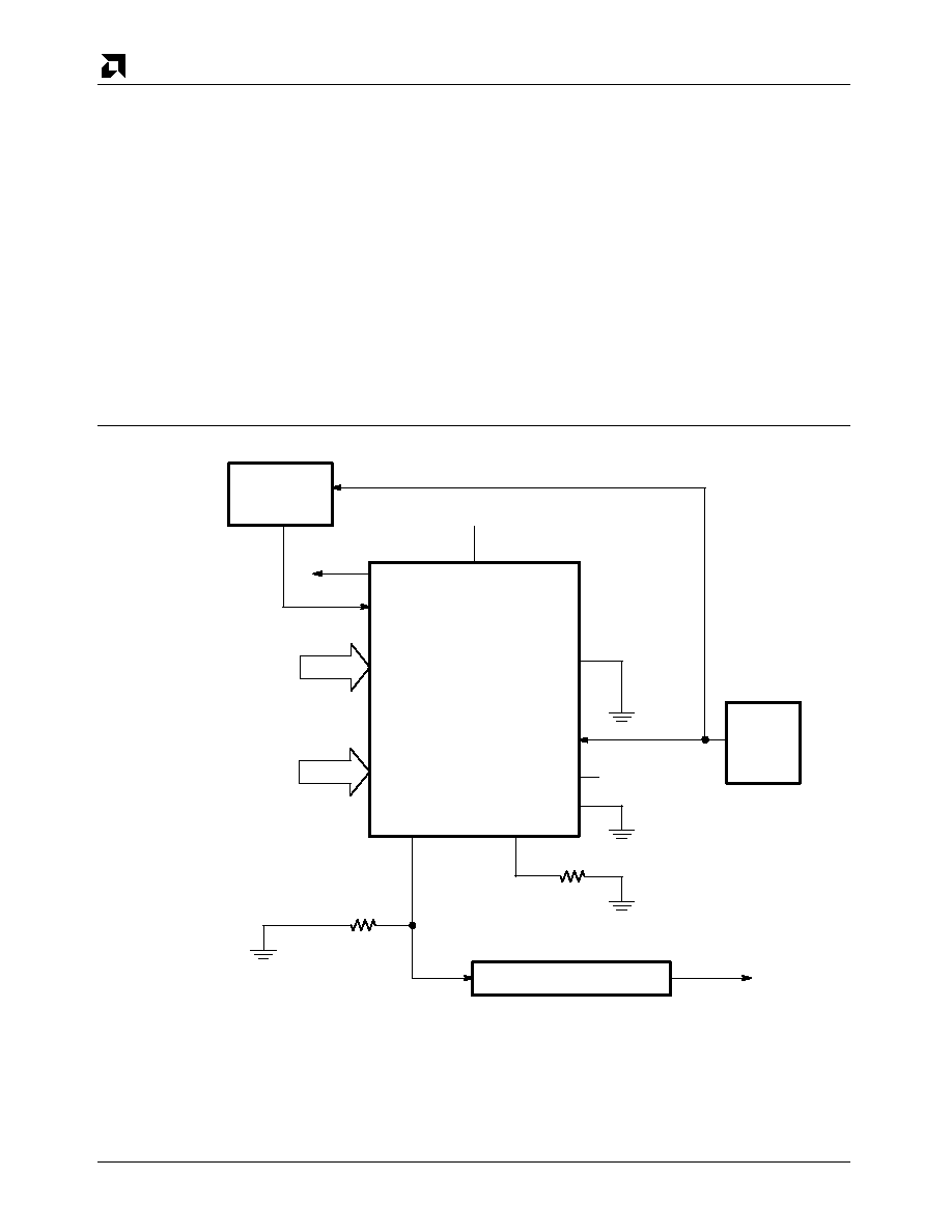
AMD
88
TAXIchip Integrated Circuits Technical Manual
This serves to flush all extraneous data from the buffers and reset all internal state
machines. Once this is completed the Transmitter may be Strobed. X1 should be left in
the LOW state upon completion of the initialization.
The STRB input must now be strobed only once every n = 10 bitclk pulses or more. This
will allow time for an 8 bit wide byte to be encoded to 10 bits and shifted out one bit
every clock pulse.
The parallel data input pins are provided with new data every 10 bitclk pulses. Setup
and hold times remain the same as in non-Test Mode with respect to STRB. (In the
non-Test modes, the clock rate is the byte rate and a new data word and a strobe is
provided every clock pulse. In test mode, the clock rate is the bit rate so the new data
word and strobe are provided every
n
clock pulses).
In Test Mode the Receiver expects only single ended data. Thus only one of the
SEROUT lines from the Transmitter is used. However, both lines must have pulldown
resistors to electrically balance the outputs.
Figure 8-1
Transmitter Test Mode Connections
ACK
STROBE
Data IN
8, 9, 10
Command IN
4, 3, 2
SEROUT+
SEROUT≠
X1
X2
RESET
CLK
CLS
DMS
300
N/C = Test Mode
Bit Rate
Clock
Generator
Divide By n
or Byte Rate
Clock
Am7968
N/C
TLS
300
Media Interface
Can Be Set
for 8, 9, or
10-Bit Mode
To Receiver
12330E-35

AMD
89
TAXIchip Integrated Circuits Technical Manual
8.2 Receiver Connections
Refer to Figure 8-2.
Grounding SERIN≠ puts the Receiver in Test Mode. SERIN+ is a single ended 100K
ECL NRZ input.
The X1 pin now becomes the bit rate clock input (bitclk), just like the CLK pin on the
Transmitter.
The CLK pin remains a
byte
rate CLK out.
8.3 Timing Relationships in Test Mode
The timing parameters in Test Mode are similar to the parameters in standard mode.
Propagation delay values remain the same, however bit time relationships are now
calculated with respect to the new bit times. For example, using a bitclk = 1.0 kHz, which
is a 1 ms period, the byte time t
35
= 10 bits x 1 ms = 10 ms. In the same way t
37
, which is
the CLK falling to STRB rising delay is now [2 (t
35
/n) + 15 ns] = 2.015 ms. Note that
Setup and Hold times for SERIN to X1 are not specified and must be determined for
each application.
Figure 8-2
Receiver Test Mode Connections
DSTRB
DATA OUT
8, 9, 10
COMMAND OUT
4, 3, 2
VLTN
SERIN+
X2
RESET
CLK
DMS
Clock Recovery
Circuit
Digital or Analog
PLL
Am7969
Normal
Function
CNB
DMS Can Be
Set For 8, 9, or
10-Bit Mode
Normal
Function
X1
SERIN≠
IGM
CMD STROBE
DATA STROBE
Single Ended
Input From
Transmitter
Byte Rate CLK Out
CSTRB
12330E-36

90
TAXIchip Integrated Circuit Technical Manual
APPENDIX A
Fiber Optic Data Link Manufacturer List
Presented below is a partial listing of fiber optic data link suppliers that manufacture or
market optical components in a data rate range compatible with the TAXIchip set.
Several of these components have been demonstrated in a bench level evaluation in
conjunction with the TAXlchip set.
AMP
1 (800) 552-6752
(416) 475-6222 (Canada)
AT&T Microelectronics
(800) 372-2447
BT&D Technologies
Delaware Corporate Center 11
Suite 200
2 Righter Parkway
Wilmington, DE 19803
(800) 545-4306
Hewlett Packard
Customer Information Center
(800) 752-0900
Sumitomo Electric
777 Old Saw Mill River Rd.
Suite 230
Tarrytown, NY 10591-6725

91
TAXIchip Integrated Circuit Technical Manual
APPENDIX B
Error Detection Efficiency
When a received data pattern does not represent a valid coding symbol, the TAXI
Receiver asserts the
VLTN
pin to indicate that the current data contains an error.
The Receiver cannot detect the occurrence of a bit error that transforms one valid
symbol into another valid but incorrect symbol. This means that the transition error can
change a valid data symbol into a different valid data symbol, or in certain cases a valid
Command symbol and not be flagged by the Violation pin.
A single noise event on the serial link can cause at a minimum a double bit error. Single
bit errors are assumed to be impossible (or at least rare) because NRZI encoding would
require that the voltage level on the link be inverted after the event. There is no known
error mechanism external to the TAXIchip set which could cause this condition. Having
confirmed that all errors are at least 2 bits wide, let us examine the location at which
these errors can exist.
Consider the 4B/5B encoded data pattern for the TAXIchip set in the 8-bit mode. The
output corresponds to two five bit nibbles for each eight bit data byte. Shown below are
four nibbles, or two bytes of encoded data output, with six possible locations for double
bit errors within nibble 1 of Byte 2.
Figure B-1
b
9
b
8
b
7
b
6
b
5
b
4
b
3
b
2
b
1
b
0
b
9
b
8
b
7
b
6
b
5
b
4
b
3
b
2
b
1
b
0
Byte 2
Byte 1
Nibble 2
Nibble 1
Nibble 2
Nibble 1
MSB
LSB MSB
LSB MSB
LSB MSB
LSB
A
B
C
D
E
F
Notes:
Error location A corresponds to a double bit error occurring in the Least Significant Bit of nibble 2 and the
Most Significant Bit of nibble 1.
Error locations B, C, D and E occur within the nibble between adjacent bits, and,
Error location F occurs between the LSB of nibble 1 (Byte 2) and the MSB of nibble 2 (Byte 1).
12330E-37

AMD
92
TAXIchip Integrated Circuit Technical Manual
For example, consider transmitting Hex
B
[1011], encoded as 10111. Error
E
occurs
changes bits b0 & b1, resulting in encoded pattern 10100, which is Hex 2 [0010]
2 bits changed, and the run length the error = 4 bits,
1 0 1 1
0 0 1 0
becomes
2 bits changed, and the run length
the error = 4 bits,
A double bit error can change valid data into a Violation, a valid Command byte, a 1-bit,
2-bit, 3-bit,or 4-bit data error. A summary of the occurrence of these errors for the six
error locations for 4B/5B encoding is summarized below in Table B1.
Table B-1
Error Type
A
B
C
D
E
F
V=5
V=5
V=5
V=3
V=3
V=1
C=5
C=3
C=5
C=3
C=5
C=1
1B=4
1B=0
1B=2
1B=4
1B=0
1B=14
2B=2
2B=8
2B=4
2B=6
2B=6
2B=0
3B=0
3B=0
3B=0
3B=0
3B=0
3B=0
4B=0
4B=0
4B=0
4B=0
4B=2
4B=0
Table B-2
Similar reasoning for the 5B/6B encoding scheme results in seven possible error
locations, and the summary of the occurrence of these errors is listed below:
A
B
C
D
E
F
G
V=13
V=16
V=12
V=6
V=9
V=10
V=5
C=3
C=2
C=2
C=4
C=3
C=4
C=3
1B=10
1B=0
1B=0
1B=0
1B=8
1B=2
1B=22
2B=6
2B=14
2B=12
2B=14
2B=12
2B=12
2B=2
3B=0
3B=0
3B=4
3B=6
3B=0
3B=0
3B=0
4B=0
4B=0
4B=2
4B=2
4B=0
4B=4
4B=0
Utilizing this information one can determine the efficiency of the violation logic in the
TAXI Receiver. Figure B2 summarizes the violation effectiveness, as well as depicting
the number of bits in error in the undetected corrupted data. This information can be
extremely useful in determining what, if any, additional error detection schemes should
be implemented. Figure B3 graphically represents the run length of the corrupted data
for the undetected errors. As shown in this figure, there are a small percentage of
unlimited run length errors. This is due to the few data patterns, which, when corrupted
will cause a false Sync pattern to be generated. This pattern will cause a running error
which will continue until the next valid Sync realigns the byte edge to its proper position.
While these
false Syncs
occur very rarely, these are the most dangerous errors in a
TAXI system, this very well may dictate the maximum user
packet
size.

AMD
93
TAXIchip Integrated Circuit Technical Manual
Figure B-2
60
50
40
30
20
10
0
Percent of
Error
Events
8 Bit
9 Bit
10 Bit
Violation
1-Bit Error
2-Bit Error
3-Bit Error
4-Bit Error
12330E-38
Figure B-3
50
40
30
20
10
0
Percent of
Undetected
Error Events
1 Bit
2 Bit
3 Bit
4 Bit
5 Bit
12330E-39
6 Bit
0.104
0.027%
0.57
Unlimited
Run Length of Error in Corrupted Data
8 Bit
9 Bit
10 Bit

94
TAXIchip Integrated Circuits Technical Manual
APPENDIX C
TAXI Technical Information Publications
The TAXI applications team has documented questions and answers that are general
purpose in nature and applicable to a wide range of applications. This documentation
has taken the form of TAXI Technical Information Publications (TlPs), and have been
incorporated in this revision of the technical manual. The contents of this appendix are
as follows:
TAXI TIP # 1:
Subject: Receiver Response to Loss of Input Signal
TAXI TIP # 2:
Subject: TAXlchip
RESET
Pin Function
TAXI TIP # 3:
Subject: Proper Use for TAXI Sync
TAXI TIP # 4:
Subject: TAXI PLL Lock-Up During Power-On!
TAXI TIP # 5:
Subject: TAXIchip set Crystal Specification
TAXI TIP # 6:
Subject: TAXI for FDDI Applications
TAXI TIP # 7:
Subject: Synchronous vs. Asynchronous Strobe
TAXI TIP # 8:
Subject: TAXI Receiver Lock Time
TAXI TIP # 9:
Subject: TAXI Bridge: Bidirectional TAXI Communication
TAXI TIP # 10:
Subject: TAXI Receiver CSTRB and DSTRB Pulse Width
TAXI TIP # 11:
Subject: Using Receiver CLK Output to Run a TAXlchip Transmitter
TAXI TIP # 12:
Subject: TAXlchip Pins Internal Circuit
TAXI TIP # 13
Subject: Demuxing a TAXIchip Receiver to Output Multi-Byte Words
TAXI TIP # 14
Subject: 32-Bit Multiplexed Cascade with the TAXIchip Transmitter
TAXI TIP # 15
Subject: General Device Information for 125/175 MHz TAXIchips
TAXI E.B. Nov `89:
Subject: TAXlchip Error Rate Example

95
TAXIchip Integrated Circuits Technical Manual
TAXI TIPs
TAXI Technical Information Publication #89-01
Subject: Receiver Response to Loss of Input Signal
Question:
It is desired that the TAXI Receiver outputs be predictable and stable during conditions
when the TAXI Transmitter may cease transmitting (power-off) or is disconnected. How
can a system designer predict the TAXI Receiver outputs or use the TAXI Receiver in a
system where the TAXI Receiver must appear
Inactive
under these conditions? This
applies to both Coaxial and Fiber-Optic Systems.
Answer:
The key to this problem is interpreting the loss of incoming Tx data as a Quiet-Line-
State and either flagging the system accordingly or gating the TAXI Receiver outputs
with an
inactive
flag.
In a Coaxial coupled system the loss of incoming signal drive will cause the TAXI
Receiver inputs to rest at the input termination bias voltages. The differential serial
inputs will normally be at equal potential. To properly interpret a loss of signal as a
constant
quiet
state the input termination bias voltages must be altered slightly from
each other. To allow reliable interpretation of the offset as a constant logic state, the
offset voltage should typically be set to about 50 mV.
The TAXI Receiver will interpret the
Quiet-Line-State
differently depending upon the
operation mode (8-bit, 9-bit, or 10-bit). In 8-bit mode the Receiver will generate continu-
ous CSTRB's with the Command outputs at F Hex, or all HIGH. In the 9-bit and 10-bit
modes there is no defined interpretation of an incoming quiet data stream. This will
cause the TAXI Receiver to generate continuous CSTRB's and the Violation output will
be continuously HIGH. A one-shot may be used to determine Violation=HIGH duration
and then generate an
inactive
flag, or the system may interpret the Violation output
directly as an
inactive
or
invalid
condition flag and halt data-dependent system opera-
tions during any byte with Violation=HIGH.
In a Fiber-Optic coupled system two methods may be used, depending on the Optical
Receiver construction. If the Optical Receiver has a
Carrier-Detect
output this signal
may be used to flag an inactive state. If there is no
Carrier-Detect
, one may be gener-
ated using an ECL one shot arrangement which will detect loss of edges after a
predetermined period of say, for example, 80 bit times. The actual time may vary
depending on the desired response to loss of data.
In either condition, if the Receiver recovered Byte Clock (CLK) is used as a system
clock, then the system must be able to tolerate a shift in the CLK frequency of typically
about +/-3% to allow for Rx-PLL offset and drift during this period. (If the Optical
Receiver begins oscillation when the fiber is dark, the TAXI Receiver PLL may attempt
to track the oscillation resulting in an indeterminate Rx recovered clock frequency.
Optical Receiver dark response thus becomes a possible system concern.)

AMD
96
TAXIchip Integrated Circuits Technical Manual
TAXI Technical Information Publication #89-02
Subject: TAXlchip RESET Pin Function
Question:
How long must the
RESET
pin be held low in order to insure that the TAXIchip has
reset?
Answer:
The
RESET
pin is level sensitive and after a LOW input level is asserted it instantane-
ously forces the Phase Lock Loop (PLL) to its lowest possible frequency (approximately
5 to 10 MHz). A 1 ms LOW pulse should allow sufficient time for the PLL to reach a
stable state. Preliminary tests conducted in the lab reported that for the full TAXI
frequency and temperature range, the time required to recover from a reset was less
than 100
µ
s.
Resetting is intended to allow graceful recovery from the rare occurrence of a PLL
lock-up due to noise bursts on the serial data lines, as may occur when light is removed
from certain optical links. In a fiber-optic coupled system, loss of optical signal may
cause the optical receiver to oscillate, causing the TAXI Receiver to track the oscillation
to an indeterminate frequency. Care must be taken to avoid the oscillation, or a reset
can be used to recover from it. After reset, the PLL begins tracking incoming data, and
the byte boundary remains undefined until the transmitted data includes a Sync (JK).
The Sync is a unique bit pattern which forces the TAXI Receiver to align itself to the
correct byte boundary.
In a coaxial system when a loss of incoming signal drive occurs, there will be no data for
the TAXI Receiver to track. This
quiet
state will be interpreted as a continuous data
pattern. The Receiver decodes this
Quiet-Line-State
differently depending upon the
operational mode selected: 8-bit, 9-bit, or 10-bit. In 8-bit mode the TAXI Receiver will
generate continuous CSTRBs with command outputs all high (
F Hex
). In 9-bit or 10-bit
modes there is no defined interpretation of an incoming quiet data stream thus generat-
ing continuous CSTRBs and forcing the violation output (VLIN) to be continuously high.
Further information on the effects of incoming signal drive loss is available in TAXI TIP
#89-01,
Receiver Response to Loss of Input Signal.

AMD
97
TAXIchip Integrated Circuits Technical Manual
TAXI Technical Information Publication #89-03
Subject: Proper Use for TAXI Sync
Question:
What is the proper use for Sync? How often is a Sync needed?
Answer:
When a Transmitter has no data to send, it sends Sync. This symbol allows the
Receiver PLL to maintain phase and frequency lock with the transmitter, exactly as
would a normal DATA stream. It has the additional special property of being a unique bit
pattern that can be used to discover the byte boundaries in an otherwise continuous
bit stream.
The Receiver PLL takes some time to achieve phase and frequency lock (as described
in section 3.3). After lock is achieved the TAXI Receiver must align the incoming data to
the proper byte boundaries. The Receiver logic compares the incoming bit stream (bit by
bit and without regard for byte boundaries) with the pattern for Sync, and when it is
found, forces an internal bit counter to
0
. The internal counter then continues to count
bits and run the byte rate logic without further reference until another Sync is found.
From this description of the Sync function, it is obvious that only
ONE
Sync symbol is
ever really required to define the byte boundary for the TAXI Receiver if the internal
counter continues to count correctly. It is unlikely that the internal logic function will
make a mistake, and therefore the counter will continue to count off the proper number
of bits per byte forever. However, there is some chance that noise can corrupt DATA
into a pattern that looks exactly like the Sync symbol. (The chance is about 0.13% of all
possible error types.) When this happens, the byte boundary is forced to an incorrect
position, and all data following is decoded incorrectly. TAXI Receiver violation detection
logic may or may not flag the errors, but the Receiver cannot distinguish properly framed
data from incorrectly framed data. The only thing that can correct this running error is
another Sync.
The minimum number of Syncs required in a user data stream is dictated by the system
sensitivity to running errors, and the system's built in error detection mechanism.
However, it is a good practice to send a Sync every 1000 bytes.
Systems that send
packetized
data, should allow a Sync between each packet. This will
assure that if an error occurs, it will be terminated at the end of the packet and will not
corrupt the succeeding packets. Systems that send data at a rate slower than the TAXI
byte rate will have Sync automatically inserted as pad characters, so the user may not
need to specifically insert them.
Systems that send
byte
or
short
phrase
data (commands or control words, for example)
might send a Sync before each
byte
or
phrase
to assure that the message is not missed
because of an earlier framing error.
From this discussion it should be clear that there is no
RIGHT NUMBER
of Syncs to
send with TAXI data. The correct number is dependent on the type of data the user is
sending, and the system sensitivity to running errors.

AMD
98
TAXIchip Integrated Circuits Technical Manual
TAXI Technical Information Publication #89-04
Subject: TAXI PLL Lock-Up During Power-On!
Question:
Is there a recommended power-on sequence for the TAXIchips to prevent PLL lock-up?
Answer:
Early versions of the -70 TAXIchips did have some sensitivities associated with hot-
plug-in lock-up, fast V
CC
rise time, and/or power supply sequencing during power-on
causing occasional PLL lock-up. These potential problems were addressed in the -125
TAXIchips with an improved circuit design. The -125 TAXIchips do not exhibit any
known power-on problems, but a PLL Reset function is available on a package pin and
may be used to restart the PLL if problems occur.
Use of the external PLL Reset pin should not be necessary with the -125 TAXIchips, but
there may be specific situations where its use may be helpful with the TAXI Receiver.
There are possible situations where large amounts of noise may occur on the Receiver
serial data inputs. Under these conditions the Rx-PLL may attempt to track the noise to
an indeterminate frequency. This deviation in frequency may adversely affect data
recovery when a good data stream reappears. System requirements may also place a
restriction on the allowed clock frequency deviation. Use of the PLL Reset function on
the Receiver may assist in the containment of some of these effects.
All V
CC
s may be powered-on simultaneously with a common supply. It is only recom-
mended that the TAXI GND pins be connected to a common Ground and the V
CC
pins
be separately filtered and decoupled to that Ground. Variations in power-on times due to
separate V
CC
filtering and decoupling are not a problem. Use of a common V
CC
supply is
sufficient as long as noise filtering of the supply at the TAXI V
CC
pins is adequate,
therefore use of separate power supplies for the V
CC
s is usually not necessary.
Refer to Section 6.1, for more information concerning power supply layout and decoupling. Further
information is also available in TAXI TIP #89-02,
TAXI Receiver RESET Pin Function.

AMD
99
TAXIchip Integrated Circuits Technical Manual
TAXI Technical Information Publication #89-05
Subject: TAXIchip Set Crystal Specification
Question:
What are the design considerations for crystals used with TAXIchip set?
Answer:
The TAXIchip's parallel mode oscillator uses a 4.0 MHz ≠ 17.5 MHz crystal with a
frequency tolerance of 0.1%.
Any crystal will oscillate in either series or parallel mode depending upon the type of
oscillator used. By specifying parallel mode and the load, the manufacturer will calibrate
the crystal in parallel mode at the desired frequency. This could be important in
applications where frequency tolerance is critical due to the fact that the resonant
frequency in parallel mode is typically 0.02% above the series mode frequency.
As discussed in section 3.3, the time required to synchronize the data recovery circuit in
the Receiver is proportional to the delta between the Transmitter frequency and the
Receiver PLL resting frequency. The Receiver resting frequency is typically less than
±
1% away from its own crystal frequency, due to mismatch between internal circuits.
The crystal specification of 0.1% is meant to be small enough to cause a negligible
effect on lock time while not increasing the crystal cost (0.025% crystals are quite
common). Sometimes tighter frequency and tolerance specifications may be necessary
to meet the user's system requirements (i.e. FIFO depth, etc.).
More information on crystal specifications for the TAXIchip set may be found in
Section 4.1.1.
A partial list of vendors follows:
Typical 12.5 MHz
Distributor
Part Number
Phone Number
I.E.A.
HC18U 12.500
(408) 435-1000
Calmax Corp.
UM-12.5
(714) 957-1299
Monitor Products
MM 49XlE12A-12.5
(619) 433-4510
Anderson Electronics
011-668-03260
(814) 695-4428
Target Electronics
CC025A-12.5
(408) 733-0384

AMD
100
TAXIchip Integrated Circuits Technical Manual
TAXI Technical Information Publication #89-06
Subject: TAXl for FDDI Applications?
Question:
Can the TAXIchip set be used for FDDI physical layer applications?
Answer:
The TAXIchip set is code compatible with the FDDI physical layer but there are restric-
tions in the design which would cause difficulty in using the TAXIchip set for the physical
layer of an FDDI node. The TAXIchip set by itself cannot be used to build a fully
compliant FDDI node, although it provides several of the functions required.
The TAXI Transmitter is compatible with FDDI at the physical layer electrical interface
and can send all codes specified by FDDI. An exception to the encoding is that Quiet-
Line-State (QLS) is defined as
fiber-dark
for FDDI, requiring a static SEROUT=LOW,
and the Transmitter defines the equivalent of QLS, as
Command
F
, as
no-transitions
,
with no control of the static logical state.
The TAXI Receiver is also compatible with FDDI at the physical layer electrical interface
and can recognize the codes specified by FDDI, with restrictions. The restrictions
concern Master-Line-State (MLS), Halt-Line-State (HLS), and the carrier detect function.
MLS and HLS are terms describing a data stream composed of a consecutive string of
HQ and HH symbols respectively, representing a
line-state
condition. The Receiver will
decode these symbols, but it does not count them to signal
line-states
as required
by FDDI.
MLS and HLS are relatively long run-length signals with 10 and 5 bit-times between
transitions respectively, as compared to a maximum limit of 3 bit-times for data. The
Receiver PLL was designed for wide operating frequency range, with tradeoffs in the
ability and time required to capture long run-length data sequences. The FDDI specifica-
tion allows 100
µ
s for the Receiver to lock upon and detect MLS following a long period
of QLS. A typical TAXI Receiver will meet these criteria but the production parts are
neither tested nor guaranteed for this condition. There are no problems associated with
tracking the MLS signal once the PLL has acquired lock.
HQ and HH, within the TAXI Receiver, require proper byte framing for detection. MLS and
HLS as specified by FDDI are not framed, therefore the transition may be located at any of
the ten bit locations. The result, as decoded within the TAXI Receiver, will be as follows:
MLS:
00100 00000
=
HQ
CMD-A
10% probability
00000 00100
=
QH
CMD-D
10% probability
all other
=
Violation
80% probability
HLS:
00100 00100
=
HH
CMD-8
20% probability
all other
=
Violation
80% probability
The FDDI line state definition does not preclude the insertion of an occasional sync
into the MLS or HLS data stream for proper framing, solving the recognition problem.
If full FDDI compliance is required, MLS and HLS must be detected external to the
TAXIchip set.
The carrier detect function, as specified by FDDI, requires the flagging of a QLS to the
MAC layer as long as the fiber is
dark
. The TAXI SERIN inputs must be static for this
condition to be met by the TAXI Receiver. This problem must be addressed directly by
the Optical receiver or gating of its outputs.
Functions of the FDDI MAC layer interface are not directly addressed in the TAXI
designs.

AMD
101
TAXIchip Integrated Circuits Technical Manual
TAXI Technical Information Publication #89-07
Subject: Synchronous vs. Asynchronous Strobe
Question:
When should synchronous vs. asynchronous strobing be employed?
Answer:
Inputs to the TAXI Transmitter can be strobed asynchronously, but with some limita-
tions. In
local
mode, the STROBE edge can rise at any time, without regard for place-
ment within any particular byte. The data associated with the STROBE (STRB) will be
latched into the Transmitter, and will be transmitted at the earliest opportunity. If some
system limitation insures that a second STRB cannot ever be within the same byte time
(80.0 ns at 125 MHz), then there is no need to observe the ACK output of the TAXI
Transmitter.
If no such guarantee exists, then ACK must be used to insure that no more than two
STRBS lie within a single byte. Again there is no restriction on STROBE placement
within a byte, since ACK will always insure that the capacity of the TAXI input buffer is
not exceeded. The TAXI input buffering can handle two STRBS within a single byte, but
this additional buffer must be
flushed
by the absence of a STRB in a given byte before
another two-strobe byte is encountered.
In an early revision of the 70 MHz Transmitter, there was a particular placement of
STROBE with respect to the falling edge of CLK, that could cause loss of data. This lead
to several revisions of technical literature mentioning the
Prohibited
Zone
, and
Uncer-
tainty Zone
. This restriction in STROBE placement has been removed in the 125 MHz
version of the Transmitter. T6 in the data sheet, now refers only to the exact placement
of the internal byte boundary. Knowledge of this time is only important for synchronous
systems to predict in which byte the data will appear.
The only restriction on Local mode asynchronous STRB input would be in systems
which require contiguous data output from the TAXI Receiver. It is possible that when
strobing asynchronously, there will be an occasional byte with no strobe, and another
nearby byte with two strobes. The Transmitter has sufficient buffering to handle this
condition, but will pad the missing byte with a Sync character. For systems that have this
restriction, STRB should be made synchronous with the CLK of Transmitter.

AMD
102
TAXIchip Integrated Circuits Technical Manual
TAXI Technical Information Publication #89-08
Subject: TAXI Receiver Lock Time
Question:
In a fully operational system in which both the Transmitter and Receiver are powered
on, how long will it take for the Receiver to lock to new data after a quiet line?
Answer:
When data transmission stops and the link becomes quiet, the TAXI Receiver PLL will
drift to its natural resting frequency which by design, is less than 3% away from the
reference frequency applied at the X1 pin.
When data appears on the line, the Receiver PLL will achieve phase lock in a time
which is proportional to the incoming data edge density and PLL loop bandwidth.
Because this lock time is dependent on the data being transmitted, the time it takes for
the receiver to lock will depend on the specific system application. In Section 3.3, three
types of data are represented and their calculated lock times are shown. By dividing the
lock time for a specific data pattern by the X1 clock period, the number of bytes to lock
the PLL can be calculated.
Because time to lock is dependent on many variables, it is represented as a typical time.
If time to lock is critical to the specific application, we suggest you allow at least the
times shown.
Although there is no guaranteed specification for time to lock, a test is run (using a JK
pattern) as part of AMD outgoing tests to ensure that all devices can achieve lock within
a reasonable time. The test is performed by sending JKs for 640
µ
s, and then without
interruption, a full rate functional test is run. For the test to pass, the PLL must lock to
the JK pattern and then track the incoming data perfectly.

AMD
103
TAXIchip Integrated Circuits Technical Manual
TAXI Technical Information Publication #89-10
Subject: TAXI Receiver CSTRB and DSTRB Pulse Width
Question:
What is the maximum CSTRB and DSTRB pulse width?
Answer:
The internal logic of the TAXI Receiver determines the pulse width of CSTRB and
DSTRB based on the timing of an internal clock (Bit Clock). Under normal conditions,
the pulse width will be 4-bit times wide in the 8-bit mode, and 5-bit times wide in the
9- and 10-bit modes. An exception to this typical width is upon re-sync which can cause
the pulse to be expanded by up to 5 bit times as the byte boundaries are re-aligned to
the incoming data stream.
The number of bit times used to represent data differs based on the operational mode;
in 8-bit mode, data is encoded into 10 bits, in 9-bit mode 11-bits, and in 10-bit mode
2 bits. For example, a Receiver operating with a 12.5 MHz crystal and utilizing 8-bit
mode will have a clock period of 80 ns (1/12.5 MHz = 80 ns). Internally the Receiver
divides this period by 10, forming the internal bit boundaries used to represent the
encoded data. This example yields a 8 ns (80 ns/10 = 8 ns) bit period, which translates
to a internal clock rate of 125 MHz (1/8 ns = 125 MHz). Figure 11. shows a timing
diagram of a TAXI Receiver internal clock and its relationship to CLK, Data, and Strobe
outputs. The Receiver utilizes this divided clock to define its internal logic states.
The CSTRB and DSTRB signals are generated by using these logic states and have a
fixed relationship to the incoming encoded data. The figure shows that from the
beginning of the byte (state 0), the CSTRB or DSTRB delay is two internal clock periods
before going high, and the signal remains high for four internal clock periods then
returns to a low logic level. Actual pulse width will vary from this ideal width due to signal
rise and fall delay, propagation delay and effects of loads external to the Receiver. The
data sheet parameters reflect these delays and normal manufacturing guard bands.

AMD
104
TAXIchip Integrated Circuits Technical Manual
Figure 11
(8-Bit Mode Example) TAXI Receiver Internal Clock Distribution
9
0
1
2
3
4
5
6
7
8
9
0
1
2
Internal
Bit
Clock
Internal
Clock
(Byte Rate)
External
Clock
(CLK)
Internal
CSTRB &
DSTRB
External
CSTRB &
DSTRB
Internal
Data
External
Data
12330E-40

AMD
105
TAXIchip Integrated Circuits Technical Manual
TAXI Technical Information Publication #89-11
Subject: Using Receiver CLK Output to Run a TAXI Transmitter
Question:
Is it possible to use the Receiver CLK output to drive the X1 input of a TAXI Transmitter?
Answer:
To assure accurate transmission of data, the Transmitter must have a stable, jitter free,
byte rate reference to its multiplying PLL. This is typically derived from a crystal and can
be connected to any crystal controlled and noise free TTL source.
The Receiver synchronizes its internal clock with the incoming signal and recovers data
and clock for use by the receiving host system.
In the process of sending high speed data over typical serial links, the data may be
affected by noise from various sources. The PLL in the Receiver removes this noise and
delivers a synchronized clock to the Receiver logic and to the host system. However,
some of the noise may feed through the PLL and appear on the CLK output. The CLK
output can jitter as much as 2 ns when recovering data from a noisy link. This will not
typically affect normal logic functions, and can be ignored. If the Receiver must realign
its byte boundary, it will stretch CLK to the new alignment position and thus protect the
host logic from shortened CLK cycles.
These noise and phase jumps make the Receiver CLK output undesirable for use as a
Transmitter frequency source.
For systems that MUST use synchronized clocks (for example to avoid FIFO re-timing
logic) it is possible to filter the Receiver CLK output and make an adequate reference for
the Transmitter.
There are two basic approaches to provide this filter. The first is to use a crystal filter
(Figure 12). When placed between the Receiver CLK and Transmitter Xl, the crystal
filter can be effective in attenuating system jitter to levels nearly comparable to crystal
controlled reference clock levels. By the nature of a crystal filter, as the frequency of the
crystal used in the filter and the data rate frequency vary, the phase of the output varies.
This will make the filter seem to have a variable delay (+ or -) which must be accommo-
dated by the users logic.
The second method is to use a PLL tracking filter (Figure 13). The jitter attenuation
through the PLL is less than that through the crystal filter because the PLL has a
bandwidth several orders of magnitude larger. The PLL provides a solution whose
merits lie between the simplicity of the crystal filter and the need for tight crystal tracking
and matching. The PLL filter is relatively straight forward. Attention to proper grounding
and board layout should be followed. The PLL filter is more tolerant of component and
environmental variations than the crystal filter.

AMD
106
TAXIchip Integrated Circuits Technical Manual
Figure 12
Crystal Filter
LT1016
Am7968
Transmitter
SEROUT +
SEROUT -
X1
X2
CLK
Am7969
Receiver
SERIN +
SERIN -
X1
X2
CLK
300
300
3
2
1
7
+5 V
4
5 6
300
Am7968
Transmitter
SEROUT +
SEROUT -
X1
X2
CLK
Am7969
Receiver
SERIN +
SERIN -
X1
X2
CLK
CLK
GND
1
µ
F
Crystal Filter
Note
:
All crystals used are of same type.
4 pF
+
-
300
12330E-41
Figure 13
PLL Filter
LMC660C
+5 V
GND
1
µ
F
Notes:
1. Filter components were chosen for the following loop parameters:
Noise Bandwidth = 10 kHz
Damping Factor = 0.5
Natural Frequency = 3.18 kHz
2. Refer to Motorola MC4024, MC4044 and National LMC660C data sheets for specifications.
+
-
V
R
V
CC
U1
D1
MC4044
GND
VCX2
OUT 2
MC4024
Am7968
TAXI
Transmitter
SEROUT +
SEROUT ≠
X1
X2
CLK
Am7969
TAXI
Receiver
SERIN +
SERIN ≠
X1
X2
CLK
GND
V
CC
GND
V+
V-
15K
15K
15K
15K
4.7K
4.7K
50
CX2
VCM2
GND
1
µ
F
50
GND
GND
50 pF
12330E-42

AMD
107
TAXIchip Integrated Circuits Technical Manual
TAXI Technical Information Publication #89-12
Subject: TAXlchip Pins Internal Circuit
Question:
What do the TAXIchip I/O circuits look like?
Answer:
There are five different input circuits and two different output circuits in the TAXIchip set.
Each I/O circuit has Electro Static Discharge (ESD) protection circuit attached to it.
The five input types are: TTL Input, ECL Input, Three State Input (TSI), High Threshold
Input (HTI), and Oscillator (OSC).
The two output types are: TTL Output and ECL Output.
Each I/O circuit and the ESD circuit are shown on the following page. The following
table lists all Transmitter and Receiver pins and their I/O type.
Pin
Pin Name
I/O Type
Pin
Pin Name
I/O Type
1
ACK
TTL OUT
1
DO3
TTL OUT
2
STRB
TTL IN
2
DO2
TTL OUT
3
SEROUT+
ECL OUT
3
DO1
TTL OUT
4
SEROUT≠
ECL OUT
4
DO0
TTL OUT
5
V
CC2
5 V
5
IGM
TTL OUT
6
V
CC1
5 V
6
RESET
HTI
7
V
CC3
5 V
7
V
CC1
5 V
8
RESET
HTI
8
V
CC2
5 V
9
DMS
TSI
9
SERIN+
ECL IN
10
CLS
TSI
10
SERIN≠
ECL IN
11
SERIN
ECL IN
11
DMS
TSI
12
CI0
TTL IN
12
DSTRB
TTL OUT
13
CI1
TTL IN
13
CSTRB
TTL OUT
14
DI9/CI2
TTL IN
14
VLTN
TTL OUT
15
DI8/CI3
TTL IN
15
CO0
TTL OUT
16
DI7
TTL IN
16
CO1
TTL OUT
17
DI6
TTL IN
17
DO9/CO2
TTL OUT
18
CLK
TTL OUT
18
DO8/CO3
TTL OUT
19
X2
OSC
19
CLK
TTL OUT
20
X1
OSC
20
GND1
GND
21
GND2
GND
21
GND2
GND
22
GND1
GND
22
X1
OSC
23
DI0
TTL IN
23
X2
OSC
24
DI1
TTL IN
24
CNB
TTL IN
25
DI2
TTL IN
25
DO7
TTL OUT
26
DI3
TTL IN
26
DO6
TTL OUT
27
DI4
TTL IN
27
DO5
TTL OUT
28
DI5
TTL IN
28
DO4
TTL OUT
Transmitter
Receiver

AMD
108
TAXIchip Integrated Circuits Technical Manual
GND
ESD
V
CC
22K
11K
GND
TTL IN
ESD
ECL IN
GND
300
300
50K
C
C
V
CC
ECL IN
ESD
TTL IN
ESD
DMS/CLS IN
V
CC
17K
9K
GND
Three-State IN
12330E-43
12330E-44
12330E-45
12330E-46

AMD
109
TAXIchip Integrated Circuits Technical Manual
V
CC
ESD
3K
3K
48K
RESET
REF.
GND
ESD
ESD
5.3K
125
125
125
GND
X1
X2
GND
HIGH Threshold IN
Oscillator
V
CC
50
ESD
GND
TTL OUT
TTL OUT
ESD
ECL OUT
V
CC
300
300
GND
ECL OUT
ESD
ECL OUT
12330E-47
12330E-48
12330E-49
12330E-50

AMD
110
TAXIchip Integrated Circuits Technical Manual
TAXI Technical Information Publication #89-13
Subject: Demuxing A TAXIchip Receiver Output to Multi-Byte Words
Question:
How can a single TAXI Receiver be used to receive multi-byte words?
Answer:
INTRODUCTION
For systems that require data reception wider than a single byte, a single TAXI Receiver
can be used to cascade the multiple bytes. This operation allows the data to be
demultiplexed from a single serial link and used by an external system.
In the following example, data is captured sequentially and output in the form of four
8-bit words. Commands, which can also be transmitted are not used in this example in
order to clarify the basics of the technique. Some simple modifications to include
commands will be presented at the end of this technical note.
The circuit shown in Figure 14 illustrates the logic configuration that has been built and
tested in the laboratory using nominal commercial parts. The circuit handles blocks of
data typically ranging from four bytes to 64K bytes.
The TAXI Receiver converts the serial information that is received by the SERIN+/≠
inputs to the data information that is output by the D0≠D7 Data pins, C0≠C3 Command
pins, and the DSTRB, CSTRB, and VLTN pins. This data information output by the
single receiver is used by the
controller
to capture the incoming data and output it four
bytes at a time.
FUNCTIONAL DESCRIPTION
Controller Circuit:
The
controller
consists of a shift register constructed of four D flip-flops and a 3-input
NOR gate. The shifter is loaded with a
1
that progresses through the flip-flops sequen-
tially clocking the first column of four registers which capture the incoming data. When
the
1
is shifted through the fourth flip-flop, it raises the PCO signal for the CLKOUT D
flip-flop. On the following rising edge of the /CLK signal the bytes of cascaded data are
simultaneously clocked out through the second column of four registers that buffer the
cascaded data to the outside system.
Controller Clock:
The clock for the
controller
circuit is generated by OR-ing DSTRB and CSTRB. This
ensures that the DSTRB signal is captured for output to the external system. These signals
also prepare the way for a simple upgrade to allow the use of commands (explained later).
Sync Commands:
When not receiving blocks of data, Sync Commands (bytes) are received which keeps
the TAXI Receiver locked onto the correct byte rate and byte boundaries. This ensures
proper capture of the data at the beginning of the next block. In addition, before a block
of data is to be sent, a Sync Command must be received to reset the counter to the
proper byte alignment and initialize the system. The Sync Commands are sent by
default in the system because they are automatically inserted whenever a byte time
passes without a STRB (no data to send) pulse at the transmitter. It is important to note
that the Receiver generates a CSTRB and outputs zeros on the Command lines when a
Sync Command is received.
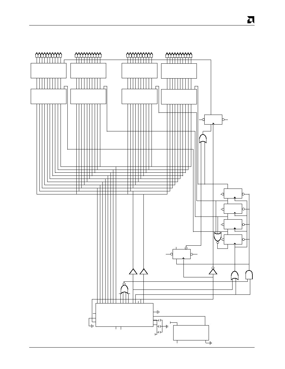
AMD
111
TAXIchip Integrated Circuits Technical Manual
12330E-51
Figure 14
Logic Diagram of Cascaded Data with One TAXI Receiver
DSTRB
VLTN
D0 -
-
-
-
-
-
D7
OE
d0
d1
d3
d2
d4 d5
d6
d7
d8
d9
GND
VCC
Y0
Y1
Y3
Y2
Y4 Y5
Y6
Y7
Y8
Y9
CP
OE
d0
d1
d3
d2
d4 d5
d6
d7
d8
d9
GND
VCC
Y0
Y1
Y3
Y2
Y4 Y5
Y6
Y7
Y8
Y9
CP
DSTRB
VLTN
D0 -
-
-
-
-
-
D7
OE
d0
d1
d3
d2
d4 d5
d6
d7
d8
d9
GND
VCC
Y0
Y1
Y3
Y2
Y4 Y5
Y6
Y7
Y8
Y9
CP
OE
d0
d1
d3
d2
d4 d5
d6
d7
d8
d9
GND
VCC
Y0
Y1
Y3
Y2
Y4 Y5
Y6
Y7
Y8
Y9
CP
DSTRB
VLTN
D0 -
-
-
-
-
-
D7
OE
d0
d1
d3
d2
d4 d5
d6
d7
d8
d9
GND
VCC
Y0
Y1
Y3
Y2
Y4 Y5
Y6
Y7
Y8
Y9
CP
OE
d0
d1
d3
d2
d4 d5
d6
d7
d8
d9
GND
VCC
Y0
Y1
Y3
Y2
Y4 Y5
Y6
Y7
Y8
Y9
CP
DSTRB
VLTN
D0 -
-
-
-
-
-
D7
OE
d0
d1
d3
d2
d4 d5
d6
d7
d8
d9
GND
VCC
Y0
Y1
Y3
Y2
Y4 Y5
Y6
Y7
Y8
Y9
CP
OE
d0
d1
d3
d2
d4 d5
d6
d7
d8
d9
GND
VCC
Y0
Y1
Y3
Y2
Y4 Y5
Y6
Y7
Y8
Y9
CP
CO0
CO1
CO2
CO3
DSTRB
CSTRB
IGM
CLM
VLTM
008
001
002
003
004
005
006
007
VCC1
VCC2
X1
X2
VCC
NC
CLR
GND
OSC
SERIN+
SERIN-
CNB
DMS
/RESET
DQ
CLK QB
CLR
PRB
DQ
CLK QB
CLR
PRB
DQ
CLK QB
CLR
PRB
DQ
QB
CLR
PRB
DQ
CLK QB
CLR
PRB
DQ
CLK QB
CLR
PRB
TAXI RX
AM7969
CHMNDO
Buffers
VCC
VCC
TAXI_CLK
/CLK
CLK_CNTR
CLR_CNTR
SYNC
CLK1
CLK2
CLK3
CLK4
Controller Block
PCD
Data Capture
Registers
Data Output
Registers
BYTE 8
BYTE 1
BYTE 2
BYTE 3
CLKOUT
4-Byte Demux Cascade Receiver
12330D-61

AMD
112
TAXIchip Integrated Circuits Technical Manual
The circuitry that handles the Sync Commands or Sync Bytes generates several signals.
The CMND0, CLR_CNTR, Sync and PCO are the signals that are generated by Sync
Command logic. The CLR_CNTR signal is generated from the CMND0 and the CSTRB
signal which signify a Sync Command has been received. CLR_CNTR clears the
controller
and then is latched by the rising edge of the Receiver CLK to form the Sync
signal. The Sync signal then generates an active PCO signal. The CLKOUT is then
driven High on the following rising edge of
CLK
if CLK4 has not already driven the
CLKOUT signal High. The Sync Command only clocks out the data when it is received
before the fourth byte of data has been received. In all other cases, the data is clocked
out by the logic involved with the fourth state of the controller. The Sync Commands that
follow this Sync Command hold the CLKOUT signal High to effectively hold the
control-
ler
circuitry in a constant state of reset with no change to the output data.
Buffering:
The buffering of signals should also be considered for this design. In this example, the
data outputs from the TAXI Receiver drive the first column of four low power registers.
This design does not exceed the driving capacity of the Receiver, but if different parts
are used, load calculations should be redone.
This system should work with any standard logic, although logic families should not be
mixed unless timing considerations have been made. This particular example uses low
power Schottky devices with relatively fast low power output registers.
TIMING CONSIDERATIONS
Some critical timing considerations must be met to ensure the proper operation of this
design. In order to capture the DSTRB signal, the timing of DSTRB going active and the
rising edge of the CLKx signals from the
controller
must agree with the setup and hold
times of the first column of registers. To ensure capture of Sync Commands, the
CLR_CNTR signal becoming active and the rising edge of the Receiver CLK must agree
with the setup and hold times of the Sync flip flop. To prevent glitches on the CLKx
signals and the potential capture of incorrect data, the timing between CLK_CNTR rising
and CLR_CNTR becoming active must be considered, CLR_CNTR needs to become
active at a time before CLK_CNTR can effect the output of CLKx. The timing diagram is
shown in Figure 16.
Figure 16 shows the timing of the system where one Sync Command is received
between data blocks being received. The premature Sync Command is not shown, but
can be derived by following the given timing diagram and known responses of the logic
given in Figure 15.
UPGRADE NOTES
Command Line Handling:
To add the capability to receive Commands in this design, only a few additions are
necessary. Since this design uses 8-bit data mode, 4-bit commands can be used. It will
be necessary to add command storage registers four bits wide as well as command
output registers four bits wide to output these Command lines correctly. The CLKx
signals as well as the CLKOUT signals for the existing registers need to be connected to
these new registers. The CLKx signals may need to be buffered to meet fanout limita-
tions of the
controller
circuitry.
Control Signals:
The signals that need to be output by the new features do not add to the logic. The
circuitry to capture the CSTRB signal is already designed into the system. The DSTRB
signal can be used as a CSTRB indicator, active Low, as well as a DSTRB indicator,

AMD
113
TAXIchip Integrated Circuits Technical Manual
active High, without any additional logic. The VLTN signal is used for both Command
and Data violations. Buffering of the DSTRB and VLTN signals may be necessary as
illustrated in Figure 15 to meet the drive requirements of the first column of registers.
Data/Command Output Note:
In this system, when a nonSync Command byte is received the data line values
corresponding to that byte will change to the values last output from the
TAXI Receiver
data lines.
Conversely, when a data byte is received the command line values for that
byte will change to the values last output from the
TAXI Receiver
command lines. This is
a characteristic of the example given and depends on how the command and data
information is latched.
Altering the Number of Output Bytes:
The above described design is an example of a four byte cascaded serial data receiving
system. The same design techniques can be used to expand or reduce the number of
bytes output at a time by the system. The considerations that should be taken into
account for an altered system deal with board space and part cost in accordance with
the requirements of the situation at hand. For board space note see the PAL Usage
section below.
PAL Usage:
In this system, the use of a PAL could greatly reduce the amount of board space used.
The PAL could incorporate all of the flip-flops and buffering logic as well as the first
column of registers that capture the system information. The reason a PAL was not
used in the system described above was to help ensure the understanding of the design
concept. For this application it is recommended that the timing considerations men-
tioned before should be investigated to ensure proper operation of the system.

AMD
114
TAXIchip Integrated Circuits Technical Manual
Figure 15
Timing Diagram of 4-Demux Cascaded Receiver
TAXI CLK
/CLK
DSTRB
CSTRB
RCVR DATA
CLKCNTR
CLK1
CLK2
CLK3
CLK4
CLKCNTR
PCO
Sync
CLKOUT
DATA OUT
Byte 4
Byte 1
Byte 2
Byte 3
Byte 4
Byte 1
Byte 2
Byte 3
4
1
2
3
4
Sync
1
2
3
Valid Data (for all four bytes)
12330E-52

AMD
115
TAXIchip Integrated Circuits Technical Manual
TAXI Technical Information Publication #89-14
Subject: 32-Bit Multiplexed Cascade with the TAXIchip Transmitter
Question:
How can a single TAXIchip Transmitter be used to send n-byte data words?
Answer:
I. INTRODUCTION
Many systems have DATA/CMD paths wider than the twelve lines available per TAXI
Transmitter. AMD TAXI applications has designed a circuit which economically multi-
plexes data words longer than eight bits using one TAXI Transmitter. The following
discussion is specifically for an Am7968 Transmitter with a 32-bit data word, but is also
applicable to systems with shorter or longer data words (with or without commands).
II. ADVANTAGES
There are several advantages to using the multiplexed data scheme utilizing one TAXI
Transmitter as opposed to a system using several Transmitters:
1) To implement the mux circuit for 32 bits requires one Am7968 TAXI Transmitter and
three relatively small integrated circuits. A 32-bit wide data path without multiplexing
requires four Am7968 TAXI Transmitters.
2) Four Am7968 TAXI Transmitters require more board real estate than three SSI parts
and one TAXI Transmitter.
3) Four Am7968 TAXI Transmitters will dissipate about 3.5 W, while one Am7968 and
three SSI chips dissipate only 1.25 W. The power saving is even more dramatic if op-
tical data links are being used. A design using four TAXI Transmitters and four
Am79h1000T optical data links would dissipate over 5 W of power. The same 32-bit
wide system using the multiplexing circuit would dissipate only 2.6 W!
III. IMPLEMENTATION
Implementation of the 32-bit multiplexed transmitter circuit is straightforward. (See
Figure 11). In addition to the Am7968 TAXI Transmitter, the following parts are required:
(1) 74LS00
(1) 74LS20
(1) 74LS174
A group of buffers with tri-state outputs (four Am29C821s in this example), would likely
be required in any type of point to point communication application and might already be
available in the host system. Additionally, a number of termination resistors are required.
The number and values are dependent upon the type of coupling and the media used.
IV. OPERATION
Referring to Figure 15, the data to be transmitted is assumed to be simultaneously
loaded into the buffers when a strobe pulse is input to the system. The controller for the
mux is the 74LS174, which is wired as a shift register. As a
0
(which occurs on strobe) is
shifted through the register, each buffer is enabled in turn. The NAND gate (U1) at the
input of D1, ensures that only a single
0
is possible while the registers are being
selected. The TAXI CLK signal, which is used to clock the 74LS174, is inverted to
provide set-up time to ensure that no false strobes reach the TAXI Transmitter. The
other four-input NAND gate (U2) enables the two-input NAND gate (U3), so that the
Transmitter will be strobed while there is data available in the buffers.

AMD
116
TAXIchip Integrated Circuits Technical Manual
Jumpers are provided on the outputs of Q4 and Q5 to be inverted (U7) and fed back to
the first NAND gate (U1). If Q4 is shorted back to the strobe input, the system will run in
auto-repeat ACK 0
mode. This means that there will be a strobe on every clock cycle. In
this mode a sync will never be sent. If the output of Q5 is shorted back to the strobe
input, the system will run in
auto-repeat ACK 1
mode. This means that a sync will be
automatically inserted in between each group of four data bytes.
On the receiver end of the link, the option is left up to the designer to either use four
Am7969 TAXI Receivers or to demultiplex the data and use only one Receiver.
Figure 16 has been included to give a detailed schematic of the circuit with an Am7969
TAXI Receiver on-board to complete the data path. Figures 17, 18, and 19 show typical
outputs for auto-run ACK0, auto-run ACK1 and Normal run modes.
V. CONCLUSION
To increase the length of a data word beyond eight bits, multiplex the data into an
Am7968 TAXI Transmitter. This method uses less power, less board space, and lowers
the parts cost of the system.

AMD
117
TAXIchip Integrated Circuits Technical Manual
12330E-53
Figure 16
32-Bit Multiplexed Transmitter Circuit
21
20
19
18
17
16
15
STRB
D0
D1
D2
D3
D4
D5
D6
D7
D8
D9
D10
D11
D12
D13
D14
D15
D16
D17
D18
D19
D20
D21
D22
D23
D24
D25
D26
D27
D28
D29
D30
D31
GND
AM29C821
GND
AM29C821
GND
AM29C821
GND
AM29C821
1A
1B
GND
1Y
1D
1C
VCC
2D
2Y
2A
2B
2C
1
2
4
5
6
7
14
13
10
9
8
12
GND
D1
D2
D3
D4
D5
D6
CLK
CLR
3
5
13
11
14
9
1
4
2
12
10
15
5
D1
D2
D3
D4
D5
D6
28
27
26
25
24
23
22
D15
D14
D13
D12
D11
D10
GND1
GND2
X1
X2
D18/C13
D17
CLK
D18
ACK
STRB
SEROUT+
SEROUT-
VCC2
VCC1
VCC3
RESET/
DMS
CLS
D19/C12
C11
SERIN
C10
1
2
3
4
5
6
7
8
9
10
11
12
13
14
1A
1B
GND
2B
2A
2Y
VCC
4B
3Y
3A
3B
4A
1Y
4Y
1
2
3
4
5
6
7
14
13
12
11
10
9
8
V
C
C
C
L
K
GND
UB
DSC
G
N
D
2
GND
3
PWR
S2
138
PWR
GND
4
S2
138
SERIN-
SERIN+
GND
U2
U10
AM7966
74LS0O
74LS2O
U9
U1
74LS174
ACK0
ACK1
U11
JMP2
U12
JMP3
4
4
4
4
4
4
4
4
1
3
5
6
7
8
9
10
11
12
24
23
22
21
20
19
18
17
16
15
14
13
OC/VCC
D0
D1
D2
D3
D4
D5
D6
D7
D8
D9
GND
Y0
Y1
Y2
Y3
Y4
Y5
Y6
Y7
Y8
Y9
CP
U6
2
4
1
3
5
6
7
8
9
10
11
12
24
23
22
21
20
19
18
17
16
15
14
13
OC/VCC
D0
D1
D2
D3
D4
D5
D6
D7
D8
D9
GND
Y0
Y1
Y2
Y3
Y4
Y5
Y6
Y7
Y8
Y9
CP
U5
2
4
1
3
5
6
7
8
9
10
11
12
24
23
22
21
20
19
18
17
16
15
14
13
OC/VCC
D0
D1
D2
D3
D4
D5
D6
D7
D8
D9
GND
Y0
Y1
Y2
Y3
Y4
Y5
Y6
Y7
Y8
Y9
CP
U4
2
4
1
3
5
6
7
8
9
10
11
12
24
23
22
21
20
19
18
17
16
15
14
13
OC/VCC
D0
D1
D2
D3
D4
D5
D6
D7
D8
D9
GND
Y0
Y1
Y2
Y3
Y4
Y5
Y6
Y7
Y8
Y9
CP
U3
2
4
To Coax or Fiber Media
12330D-63

AMD
118
TAXIchip Integrated Circuits Technical Manual
Figure 17
AUTORUN ACK 0 (No Sync Between Data Bytes)
12330E-54
D
7
D
6
D
5
D
4
D
3
D
2
D
1
D
0
STRB
TXCLK
DSTRB
CSTRB
Figure 18
AUTORUN ACK 1 (One Sync Between Every Four Data Bytes)
TXCLK
12330E-55
D
7
D
6
D
5
D
4
D
3
D
2
D
1
D
0
STRB
DSTRB
CSTRB

AMD
119
TAXIchip Integrated Circuits Technical Manual
Figure 19
Normal Run Mode (Transmission of Syncs Depends on Host)
12330E-56
D
7
D
6
D
5
D
4
D
3
D
2
D
1
D
0
STRB
TXCLK
DSTRB
CSTRB

AMD
120
TAXIchip Integrated Circuits Technical Manual
TAXI Technical Information Publication #89-15
Subject: General Device Information for 125/175 MHz TAXIchips
This T.I.P. provides general information about the design and manufacturing of the
125 MHz and 175 MHz TAXIchips. The information is separated into three categories:
Design, Wafer Fab, and Assembly/Packaging.
Design:
Transmitter (TX)
Receiver (RX)
Product P/N:
Am7968-125
Am7969-125
Am7968-175
Am7969-175
Die Number:
4768
4769
Chip Dimensions:
170 x 167 mils
2
196 x 187 mils
2
# NPN Transistors:
3386
4384
# PNP Transistors:
14
24
# Resistors:
2504
3556
# Diodes:
87
76
Equiv. Gate Count:
595
720
I/O Schematics:
See TAXI TIP #89-12
Supply Currents:
Typical Values (mA), V
CC
= 5.5 V Process=Nominal, CD 028 package,
Temp. forced with moving air flow (approx. theta
JMA
= 20
∞
C/W)
≠55
∞
C
0
∞
C
25
∞
C
70
∞
C
125
∞
C
Transmitter:
230
215
203
187
178
Receiver:
272
250
237
212
182
Wafer Fab:
Location:
Fab 2A, San Antonio, TX (formerly Fab 11) Process ID:
Bipolar IMOX≠S2: 402L≠1156
Metal One:
TiW (barrier metal): 1800 A nom. thickness AlCu: 1.0% Cu,
8000 A nom. thickness Pitch = 4
µ
Metal Two:
AlCu: 1.0% Cu, 15500 A nom. thickness Pitch = 8
µ
Passivation:
Silox/Nitride dual layer.
7500 A nominal thickness Nitride: 6800 A nominal thickness

AMD
121
TAXIchip Integrated Circuits Technical Manual
Assembly/Packaging:
CerDIP (CD 028)
LCC (CLT028)
PLCC (PL 028)
Assembly Location:
Manila
Bangkok
Ld. Frame Material:
CD: Alloy 42
Copper
Bond Wire:
1.25 mil
1.25 mil Au
Al/Si (1% Si)
Bonding Method:
Ultrasonic
Ball Bonding
Die Attach:
Ag Glass
Ag Filled Epoxy
Molding Compound:
N/A
Sumitomo 6300H
Lead Finish
CD 028 Comm.:
Tin Plate
CD 028 Mil.:
Solder Dip
CLT028 Mil.:
Solder Dip
PL 028:
Solder Plate
Thermal Impedance:
CD 028
1
CLT028
2
PL 028
2
JA
TX :
41
∞
C/W
n/a
53
∞
C/W
RX:
43
∞
C/W
n/a
52
∞
C/W
JC
TX, RX:
4
∞
C/W
10
∞
C/W
12
∞
C/W
1
socketed
2
surface mounted

AMD
122
TAXIchip Integrated Circuits Technical Manual
TAXI Technical Information Publication #89-Nov '89
Subject: TAXIchip Error Rate Example
INTRODUCTION
A method was devised to establish a baseline TAXIchip set error rate. A series of tests
were conducted at a transmission rate of 125 MHz at room temperature, and various
power supply voltages. The data collected will be used to determine fiber optic and wire
interconnect BER (Bit Error Rate) tests to be completed at a later date.
METHOD
The test method used the TAXI Transmitters and Receivers to transfer data continu-
ously for at least one thousand hours per pair with different V
CC
conditions. To imple-
ment this test, five TAXI K2 boards were used. Each board includes a TAXI Transmitter
with a ROM data source, and a Receiver with a ROM data checker to test data integrity
on every byte. They were set up according to the diagrams in Figure 20, and intercon-
nected with AC coupled short coax lines.
In Setup 1, a single power supply with 5 V V
CC
was attached to TAXI K2 board #1.
Board #1 ran independently with the SEROUT+/≠ connected to its SERIN+/≠ with 50
coaxial cables.
Setup 2 had oscillating voltages (4 V to 6 V) connected to the V
CC
of TAXI K2 boards #2
and #3. The SEROUT+/≠ of board #2 were connected to the SERIN+/≠ of board #3, and
the SEROUT+/≠ of board #3 connected to the SERIN+/≠ of board #2, with 50
coaxial
cables, forming two test setups with continually varying power supply voltages.
Setup 3 also uses two power supplies with one set at 4 V and the other at 6 V. These
two power supplies were connected to TAXI K2 boards #4 and #5. The SEROUT+/- and
SERIN+/- were connected in the same configuration as boards #2 and #3 in setup 2 with
50
coaxial cables.
The power supply voltages used (4 and 6 V) are outside the data sheet specification for
the TAXIchip set. This test was intended to stress the parts and to simulate extreme
temperature and operating conditions.
These five boards were checked regularly, and the error counts were recorded. To verify
that these boards were still running correctly, they were made to fail intentionally and
then reset.
RESULT
The tests were completed after each board ran more than 1,000 hours. The table below
summarizes the results.
Board#
Hours
Errors
Notes
1
1,606
0
2
1,623
8*
Errors occurred between 438≠558 hours
3
1,082
0
4
1,607
2*
Errors occurred between 438≠558 hours
5
1,082
0
.
* One error can cause multiple error counts. These were assumed to be one error event.

AMD
123
TAXIchip Integrated Circuits Technical Manual
Board #4 failed on another occasion after the errors indicated above, but this failure was
due to a power supply failure. Failure time was subtracted from the total run time, and
errors were not indicated in the total. Also, boards #2 and #4 ran over 1,000 hours each
without any error after the only noted error occurrence.
CONCLUSION
The fives sets of TAXI Transmitters and Receivers have run a sum total of 7,000 hours
(3.15 x 10
14
bytes) with two error events.
Figure 20
TAXI K2 Board Transmit/Receive Section
TAXI
TX
ROM
TAXI
TX
ROM and
Comparator
A
B
12330E-57
V
CC
V
CC
Note:
TAXI K2 board includes both
TAXI TX
and
TAXI RX
. Each half may be used independently or with other
boards with matching ROM data patterns. For the test described above, FDDI DDJ ROM patterns were used.
TAXI TX
TAXI RX
SETUP 1
5
5
SETUP 2
4≠6 Variable
4≠6 Variable
4≠6 Variable
4≠6 Variable
SETUP 3
4
6
6
4
V
CC
Conditions