AMENDMENT
This document contains information on a product under development at Advanced Micro Devices. The information
is intended to help you evaluate this product. AMD reserves the right to change or discontinue work on this product
without notice.
Publication# 16514
Rev: D Amendment/1
Issue Date: October 1998
80C186 and 80C188 Integrated
16-Bit Microprocessors
This document amends the
80C186 and 80C188 Integrated 16-Bit Microprocessors Data Book
, order #16514D, and
replaces the discontinued
80C186/80C188 CMOS High-Integration 16-Bit Microprocessors Amendment
(specifica-
tions for the 20-MHz industrial operating range). This amendment consists of two parts:
n
Clock generation information changes for the 80C186 and 80C188 microcontrollers. If the guidelines in this bulletin
are not followed, you may experience problems with clock start-up.
n
Industrial operating information at 20 MHz. This is the same information that was published in the discontinued
80C186/80C188 CMOS High-Integration 16-Bit Microprocessors Amendment
.
CLOCKING INFORMATION CHANGES
Crystal-Driven Clock Source
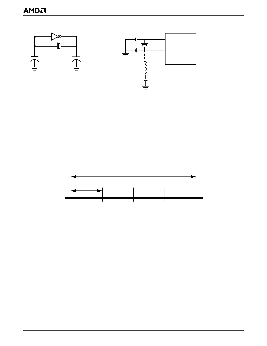
The internal oscillator circuit of the microcontroller is
d e s i g n e d t o f u n c ti o n w i t h a p a r a l l e l re s o n a n t
fundamental or third-overtone crystal. The 80C186 and
80C188 microprocessors use a crystal frequency that
is twice the processor frequency. AMD does not
recommend that you replace a crystal with an LC or RC
equivalent for any member of the Am186TM family.
The X1 and X2 signals are connected to an internal
inverting amplifier (oscillator) that provides, along with
the external feedback loading, the necessary phase
shift (Figure 1 on page 2). In such a positive feedback
circuit, the inverting amplifier has an output signal (X2)
180 degrees out of phase of the input signal (X1). The
external feedback network provides an additional 180
degree phase shift. In an ideal system, the input to X1
has 360 or zero degrees of phase shift.
The external feedback network is designed to be as
close as possible to ideal. If the feedback network is not
providing necessary phase shift, negative feedback
dampens the output of the amplifier and negatively
affects the operation of the clock generator. Values for
the loading on X1 and X2 must be chosen to provide
the necessary phase shift and crystal operation.
Selecting a Crystal
When selecting a crystal, you should always specify the
load capacitance (C
L
). This value can cause variance in
the oscillation frequency from the desired specified value
(resonance). The load capacitance and the loading of the
feedback network have the following relationship:
C
L
= (( C
1
∑ C
2
)/( C
1
+ C
2
)) + C
S
where C
S
is the stray capacitance of the circuit. Placing
the crystal and C
L
in series across the inverting
amplifier and tuning these values (C
1
, C
2
) allows the
crystal to oscillate at resonance. This relationship is
true for both fundamental and third-overtone operation.
Finally, there is a relationship between C
1
and C
2
. To
enhance the oscillation of the inverting amplifier, these
values must be offset with the larger load on the output
(X2). Equal values of these loads tend to balance the
poles of the inverting amplifier.
The characteristics of the inverting amplifier set limits
on the following parameters for crystals:
ESR (Equivalent Series Resistance) ........... 40
Max
Drive Level .................................................. 1 mW Max
The recommended range of values for C1and C2 are
as follows:
C
1
............................................................. 15 pF ± 20%
C
2
............................................................. 22 pF ± 20%
You must determine the specific values for C
1
and C
2
.
The values are dependent on the characteristics of the
chosen crystal and board design. The C
1
and C
2
values include the stray capacitances of the design.
Figure 1 on page 2 shows the correct connection of the
oscillator configurations. Figure 1a shows the inverting
amplifier configuration. This is the equivalent circuitry
with the inverter integrated into the microcontroller.
Figure 1b shows the crystal configuration. The diagram
shows the correct connection for third-overtone
crystals. The fundamental mode crystals do not require
the L
1
or the 200-pF capacitor. Figure 1c shows the
recommended crystal mode based on the crystal
frequency. The 80C186 and 80C188 microprocessors
use a crystal twice the CPU frequency and can use
either fundamental or third-overtone mode crystals,
depending on the CPU frequency.

80C186 and 80C188 Integrated 16-Bit Microprocessors Data Book Amendment
3
A M E N D M E N T
SWITCHING CHARACTERISTICS OVER INDUSTRIAL OPERATING RANGE AT 20 MHZ
This section includes the following timings and timing waveforms at 20 MHz:
n
"Read-Cycle Timings" on page 4
n
"Read-Cycle Waveforms" on page 5
n
"Write-Cycle Timings" on page 6
n
"Write-Cycle Waveforms" on page 7
n
"Interrupt Acknowledge Cycle Timings" on page 8
n
"Interrupt Acknowledge Cycle Waveforms" on page 9
n
"Software Halt Cycle Timings" on page 10
n
"Software Halt Cycle Waveforms" on page 11
n
"Clock Timings" on page 12
n
"Clock Waveforms" on page 13
n
"Ready, Peripheral, and Queue Status Timings" on page 14
n
"Synchronous Read (SRDY) Waveforms" on page 14
n
"Asynchronous Ready (ARDY) Waveforms" on page 15
n
"Peripheral and Queue Status Waveforms" on page 15
n
"RESET and HOLD/HLDA Timings" on page 16
n
"RESET Waveforms" on page 16
n
"HOLD/HLDA Waveforms (Entering HOLD)" on page 17
n
"HOLD/HLDA Waveforms (Leaving HOLD)" on page 17
4
80C186 and 80C188 Integrated 16-Bit Microprocessors Data Book Amendment
A M E N D M E N T
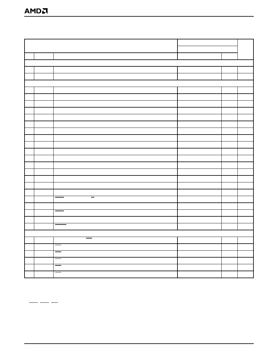
Read-Cycle Timings
1
T
A-IND
=≠40
∞
C to +85
∞
C, V
CC
=5 V
±
10%
Notes:
1. All timings are measured at 1.5 V and 100-pF loading on CLKOUT unless otherwise noted. All output test conditions are with
C
L
= 50≠100 pF (10≠20 MHz). For AC tests, input V
IL
= 0.45 V and V
IH
= 2.4 V, except at X1 where V
IH
= V
CC
≠ 0.5 V.
Preliminary
Parameter
20 MHz
#
Symbol
Description
Min
Max
Unit
General Timing Requirements (listed more than once)
1
t
DVCL
Data in Setup (A/D)
10
ns
2
t
CLDX
Data in Hold (A/D)
3
ns
General Timing Responses (listed more than once)
3
t
CHSV
Status Active Delay
3
29
ns
4
t
CLSH
Status Inactive Delay
3
29
ns
5
t
CLAV
Address Valid Delay
3
25
ns
6
t
CLAX
Address Hold
0
ns
7
t
CLDV
Data Valid Delay
3
25
ns
8
t
CHDX
Status Hold Time
10
ns
9
t
CHLH
ALE Active Delay
20
ns
10
t
LHLL
ALE Width
t
CLCL
≠15 = 35
ns
11
t
CHLL
ALE Inactive Delay
20
ns
12
t
AVLL
Address Valid to ALE Low
2
2. Equal loading.
t
CLCH
≠10 = 10
ns
13
t
LLAX
Address Hold from ALE Inactive
2
t
CHCL
≠10 = 10
ns
14
t
AVCH
Address Valid to Clock High
0
ns
15
t
CLAZ
Address Float Delay
t
CLAX
= 0
17
ns
16
t
CLCSV
Chip-Select Active Delay
3
25
ns
17
t
CXCSX
Chip-Select Hold from Command Inactive
2
t
CLCH
≠10 = 10
ns
18
t
CHCSX
Chip-Select Inactive Delay
3
20
ns
19
t
DXDL
DEN Inactive to DT/R Low
0
ns
20
t
CVCTV
Control Active Delay 1
3
3. DEN, INTA, WR.
3
22
ns
21
t
CVDEX
DEN Inactive Delay
3
22
ns
22
t
CHCTV
Control Active Delay 2
3
3
22
ns
23
t
CLLV
LOCK Valid/Invalid Delay
3
22
ns
Timing Responses (Read Cycle)
24
t
AZRL
Address Float to RD Active
0
ns
25
t
CLRL
RD Active Delay
3
27
ns
26
t
RLRH
RD Pulse Width
2t
CLCL
≠20 = 80
ns
27 t
CLRH
RD Inactive Delay
3
25
ns
28
t
RHLH
RD Inactive to ALE High
2
t
CLCH
≠10 = 10
ns
29
t
RHAV
RD Inactive to Address Active
2
t
CLCL
≠15 = 35
ns