PRELIMINARY
Publication# 21195
Rev: B Amendment/+2
Issue Date: April 1998
Am29F017B
16 Megabit (2 M x 8-Bit)
CMOS 5.0 Volt-only, Uniform Sector Flash Memory
DISTINCTIVE CHARACTERISTICS
s
Optimized for memory card applications
-- Backwards-compatible with the Am29F016C
s
5.0 V
±
10%, single power supply operation
-- Minimizes system level power requirements
s
Manufactured on 0.35
µm process technology
s
High performance
-- Access times as fast as 70 ns
s
Low power consumption
-- 25 mA typical active read current
-- 30 mA typical program/erase current
-- 1
µ
A typical standby current (standard access
time to active mode)
s
Flexible sector architecture
-- 32 uniform sectors of 64 Kbytes each
-- Any combination of sectors can be erased.
-- Supports full chip erase
-- Group sector protection:
A hardware method of locking sector groups to
prevent any program or erase operations within
that sector group
Temporary Sector Group Unprotect allows code
changes in previously locked sectors
s
Embedded Algorithms
-- Embedded Erase algorithm automatically
preprograms and erases the entire chip or any
combination of designated sectors
-- Embedded Program algorithm automatically
writes and verifies bytes at specified addresses
s
Minimum 1,000,000 program/erase cycles per
sector guaranteed
s
Package options
-- 48-pin TSOP
s
Compatible with JEDEC standards
-- Pinout and software compatible with
single-power-supply Flash standard
-- Superior inadvertent write protection
s
Data# Polling and toggle bits
-- Provides a software method of detecting
program or erase cycle completion
s
Ready/Busy# output (RY/BY#)
-- Provides a hardware method for detecting
program or erase cycle completion
s
Erase Suspend/Erase Resume
-- Suspends a sector erase operation to read data
from, or program data to, a non-erasing sector,
then resumes the erase operation
s
Hardware reset pin (RESET#)
-- Resets internal state machine to the read mode

2
Am29F017B
P R E L I M I N A R Y
GENERAL DESCRIPTION
The Am29F017B is a 16 Mbit, 5.0 volt-only Flash mem-
ory organized as 2,097,152 bytes. The 8 bits of data
appear on DQ0≠DQ7. The Am29F017B is offered in a
48-pin TSOP package. This device is designed to be
programmed in-system with the standard system 5.0
volt V
CC
supply. A 12.0 volt V
PP
is not required for pro-
gram or erase operations. The device can also be pro-
grammed in standard EPROM programmers.
This device is manufactured using AMD's 0.35
µ
m
process technology, and offers all the features and ben-
efits of the Am29F016C, which was manufactured
using 0.5
µ
m process technology.
The standard device offers access times of 70, 90, 120,
and 150 ns, allowing high-speed microprocessors to
operate without wait states. To eliminate bus conten-
tion, the device has separate chip enable (CE#), write
enable (WE#), and output enable (OE#) controls.
The device requires only a single 5.0 volt power sup-
ply for both read and write functions. Internally gener-
ated and regulated voltages are provided for the
program and erase operations.
The device is entirely command set compatible with the
JEDEC single-power-supply Flash standard. Com-
mands are written to the command register using stan-
dard microprocessor write timings. Register contents
serve as input to an internal state-machine that con-
trols the erase and programming circuitry. Write cycles
also internally latch addresses and data needed for the
programming and erase operations. Reading data out
of the device is similar to reading from other Flash or
EPROM devices.
Device programming occurs by executing the program
command sequence. This initiates the Embedded
Program algorithm--an internal algorithm that auto-
matically times the program pulse widths and verifies
proper cell margin.
Device erasure occurs by executing the erase com-
mand sequence. This initiates the Embedded Erase
algorithm--an internal algorithm that automatically
preprograms the array (if it is not already programmed)
before executing the erase operation. During erase, the
device automatically times the erase pulse widths and
verifies proper cell margin.
The host system can detect whether a program or
erase operation is complete by observing the RY/BY#
pin, or by reading the DQ7 (Data# Polling) and DQ6
(toggle) status bits. After a program or erase cycle has
been completed, the device is ready to read array data
or accept another command.
The sector erase architecture allows memory sectors
to be erased and reprogrammed without affecting the
data contents of other sectors. The device is fully
erased when shipped from the factory.
Hardware data protection measures include a low
V
CC
detector that automatically inhibits write opera-
tions during power transitions. The hardware sector
protection feature disables both program and erase
operations in any combination of the sectors of mem-
ory. This can be achieved via programming equipment.
The Erase Suspend feature enables the user to put
erase on hold for any period of time to read data from,
or program data to, any sector that is not selected for
erasure. True background erase can thus be achieved.
The hardware RESET# pin terminates any operation
in progress and resets the internal state machine to
reading array data. The RESET# pin may be tied to the
system reset circuitry. A system reset would thus also
reset the device, enabling the system microprocessor
to read the boot-up firmware from the Flash memory.
The system can place the device into the standby
mode. Power consumption is greatly reduced in
this mode.
AMD's Flash technology combines years of Flash
memory manufacturing experience to produce the
h i g h e s t l eve l s o f q u a l i t y, r e l i a b i l i t y a n d c o s t
effectiveness. The device electrically erases all
b i t s w i t h i n a s e c t o r s i m u l t a n e o u s l y v i a
F o w l e r -N o r d h e i m t u n n e l i n g . T h e d a t a i s
programmed using hot electron injection.
4
Am29F017B
P R E L I M I N A R Y
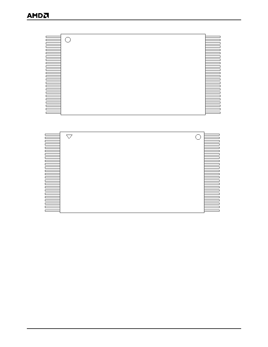
CONNECTION DIAGRAMS
1
24
2
3
4
5
6
7
8
9
10
11
12
13
14
15
16
17
18
19
20
21
22
23
NC
NC
NC
A19
A18
A17
A16
A15
A14
A13
A12
CE#
V
CC
NC
RESET#
A11
A10
A9
A8
A7
A6
A5
A4
NC
48
25
47
46
45
44
43
42
41
40
39
38
37
36
35
34
33
32
31
30
29
28
27
26
NC
NC
NC
A20
NC
WE#
OE#
RY/BY#
DQ7
DQ6
DQ5
DQ4
V
CC
V
SS
V
SS
DQ3
DQ2
DQ1
DQ0
A0
A1
A2
A3
NC
48-Pin Standard TSOP
21195B-2
1
24
2
3
4
5
6
7
8
9
10
11
12
13
14
15
16
17
18
19
20
21
22
23
NC
NC
NC
A20
NC
WE#
OE#
RY/BY#
DQ7
DQ6
DQ5
DQ4
V
CC
V
SS
V
SS
DQ3
DQ2
DQ1
DQ0
A0
A1
A2
A3
NC
48
25
47
46
45
44
43
42
41
40
39
38
37
36
35
34
33
32
31
30
29
28
27
26
NC
NC
NC
A19
A18
A17
A16
A15
A14
A13
A12
CE#
V
CC
NC
RESET#
A11
A10
A9
A8
A7
A6
A5
A4
NC
48-Pin Reverse TSOP
21195B-3