
PRELIMINARY
This document contains information on a product under development at Advanced Micro Devices. The information
is intended to help you evaluate this product. AMD reserves the right to change or discontinue work on this proposed
product without notice. AMD, the AMD logo, and combinations thereof are trademarks of Advanced Micro Devices,
Inc.
Publication# 21336
Rev: A Amendment/0
Issue Date: May 1997
D
R
A
F T
Am186
TM
ED/EDLV
High Performance, 80C186- and 80C188-Compatible,
16-Bit Embedded Microcontrollers
DISTINCTIVE CHARACTERISTICS
n
E86
TM
family 80C186- and 80C188-compatible
microcontroller with enhanced bus interface
≠ Lower system cost with higher performance
≠ 3.3-V ± 0.3-V operation (Am186EDLV
microcontrollers)
n
Programmable DRAM Controller
≠ Supports zero-wait-state operation with 50-ns
DRAM at 40 MHz, 60-ns @ 33 MHz, 70-ns @ 25
MHz
≠ Includes programmable CAS-before-RAS
refresh capability
n
High performance
≠ 20-, 25-, 33-, and 40-MHz operating frequencies
≠ Zero-wait-state operation at 40 MHz with 70-ns
static memory
≠ 1-Mbyte memory address space
≠ 64-Kbyte I/O space
n
Enhanced features provide improved memory
access and remove the requirement for a 2x clock
input
≠ Nonmultiplexed address bus
≠ Processor operates at the clock input frequency
≠ 8-bit or 16-bit programmable bus sizing including
8-bit boot option
n
Enhanced integrated peripherals
≠ 32 programmable I/O (PIO) pins
≠ Two full-featured asynchronous serial ports allow
full-duplex, 7-bit, 8-bit, or 9-bit data transfers
≠ Serial port hardware handshaking with CTS,
RTS, ENRX, and RTR selectable for each port
≠ Improved serial port operation enhances 9-bit
DMA support
≠ Independent serial port baud rate generators
≠ DMA to and from the serial ports
≠ Watchdog timer can generate NMI or reset
≠ A pulse-width demodulation option
≠ A data strobe, true asynchronous bus interface
option included for DEN
≠ Reset configuration register
n
Familiar 80C186 peripherals
≠ Two independent DMA channels
≠ Programmable interrupt controller with up to 8 ex-
ternal and 8 internal interrupts
≠ Three programmable 16-bit timers
≠ Programmable memory and peripheral
chip-select logic
≠ Programmable wait state generator
≠ Power-save clock divider
n
Software-compatible with the 80C186 and
80C188 microcontrollers with widely available
native development tools, applications, and
system software
n
A compatible evolution of the Am186EM,
Am186ES, and Am186ER microcontrollers
n
Available in the following packages:
≠ 100-pin, thin quad flat pack (TQFP)
≠ 100-pin, plastic quad flat pack (PQFP)
GENERAL DESCRIPTION
The Am186
TM
ED/EDLV microcontrollers are part of the
AMD E86
TM
family of embedded microcontrollers and mi-
croprocessors based on the x86 architecture. The
Am186ED/EDLV microcontrollers are the ideal upgrade
for 80C186/188 designs requiring 80C186/188 compat-
ibility, increased performance, serial communications, a
direct bus interface, and more than 64K of memory.
The Am186ED/EDLV microcontrollers integrate a com-
plete DRAM controller to take advantage of low DRAM
costs. This reduces memory subsystem costs while
maintaining SRAM performance.The Am186ED/EDLV
microcontrollers also integrate the functions of a CPU,
nonmultiplexed address bus, three timers, watchdog
timer, chip selects, interrupt controller, two DMA control-
lers, two asynchronous serial ports, programmable bus
sizing, and programmable I/O (PIO) pins on one chip.
Compared to the 80C186/188 microcontrollers, the
Am186ED/EDLV microcontrollers enable designers to
reduce the size, power consumption, and cost of em-
bedded systems, while increasing reliability, functional-
ity, and performance.
The Am186ED/EDLV microcontrollers have been
designed to meet the most common requirements of
embedded products developed for the communications,
o ff i c e a u t o m a t i o n , m a s s s t o r a g e , a n d g e n e ra l
embedded markets. Specific applications include
PBXs, multiplexers, modems, disk drives, hand-held
and desktop terminals, fax machines, printers,
photocopiers, and industrial controls.
Am186ED/EDLV Microcontrollers
3
P R E L I M I N A R Y
D
R
A
F T
ORDERING INFORMATION
Standard Products
AMD standard products are available in several packages and operating ranges. The order number (valid combination) is formed
by a combination of the elements below.
≠20 = 20 MHz
≠25 = 25 MHz
≠33 = 33 MHz
≠40 = 40 MHz
TEMPERATURE RANGE
C= ED Commercial (T
C
=0
∞
C to +100
∞
C)
C = EDLV Commercial (T
C
=0
∞
C to +70
∞
C)
I = ED Industrial (T
A
=≠40
∞
C to +85
∞
C)
where: T
C
= case temperature
where: T
A
= ambient temperature
SPEED OPTION
DEVICE NUMBER/DESCRIPTION
LEAD FORMING
\W=Trimmed and Formed
Valid combinations list configurations planned to be
supported in volume for this device. Consult the
local AMD sales office to confirm availability of
specific valid combinations and to check on newly
released combinations.
Note: The industrial version of the Am186ED as
well as the Am186EDLV are available in 20 and 25
MHz operating frequencies only.
The Am186ED and Am186EDLV microcontrollers
are all functionally the same except for their DC
characteristics and available frequencies.
Note: There is no 188 version of the Am186ED/
EDLV. The same 8-bit external bus capabilities
can be achieved using the 8-bit boot capability and
programmable bus sizing options.
Valid Combinations
PACKAGE TYPE
V=100-Pin Thin Quad Flat Pack (TQFP)
K=100-Pin Plastic Quad Flat Pack (PQFP)
Am186ED = High-Performance, 80C186-Compatible,
16-Bit Embedded Microcontroller
Am186EDLV = High-Performance, 80L186-Compatible,
Low-Voltage, 16-Bit Embedded Microcontroller
Am186EDLV≠25
Valid Combinations
Am186EDLV≠20
VC\W or
KC\W
Am186ED≠25
Am186ED≠33
Am186ED≠40
Am186ED≠20
KI\W
1
Am186ED≠25
Am186ED≠20
VC\W or
KC\W
Note:
The industrial version of the Am186ED is
offered only in the PQFP package.
-40
K
C
\W
Am186
TM
ED/EDLV

4
Am186ED/EDLV Microcontrollers
P R E L I M I N A R Y
D
R
A
F T
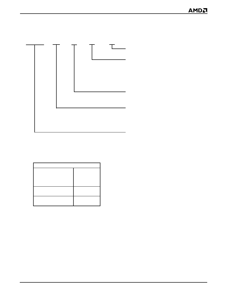
TABLE OF CONTENTS
DISTINCTIVE CHARACTERISTICS ........................................................................................... 1
GENERAL DESCRIPTION .......................................................................................................... 1
AM186ED/EDLV MICROCONTROLLERS BLOCK DIAGRAM ................................................... 2
ORDERING INFORMATION ....................................................................................................... 3
Standard Products ........................................................................................................... 3
RELATED AMD PRODUCTS ...................................................................................................... 9
E86
TM
Family Devices ...................................................................................................... 9
Related Documents ....................................................................................................... 10
Third-Party Development Support Products .................................................................. 10
Customer Service .......................................................................................................... 10
KEY FEATURES AND BENEFITS ............................................................................................ 10
Application Considerations .............................................................................................11
COMPARING THE AM186ED/EDLV TO THE AM186ES/ESLV MICROCONTROLLERS ........ 12
Integrated DRAM Controller ........................................................................................... 12
Enhanced Refresh Control Unit ..................................................................................... 13
Option to Overlap DRAM with PCS ............................................................................... 13
Additional Serial Port Mode for DMA Support of 9-bit Protocols .................................... 13
Option to Boot from 8- or 16-bit Memory ....................................................................... 13
Improved External Bus Master Support ......................................................................... 13
PSRAM Controller Removed ......................................................................................... 13
TQFP CONNECTION DIAGRAMS AND PINOUTS .................................................................. 14
Top Side View--100-Pin Thin Quad Flat Pack (TQFP) ................................................. 14
TQFP PIN DESIGNATIONS ....................................................................................................... 15
Sorted by Pin Number .................................................................................................... 15
Sorted by Pin Name ....................................................................................................... 16
PQFP CONNECTION DIAGRAMS AND PINOUTS .................................................................. 17
Top Side View--100-Pin Plastic Quad Flat Pack (PQFP) ............................................. 17
PQFP PIN DESIGNATIONS ....................................................................................................... 18
Sorted by Pin Number .................................................................................................... 18
Sorted by Pin Name ....................................................................................................... 19
LOGIC SYMBOL--AM186ED/EDLV MICROCONTROLLERS ................................................. 20
PIN DESCRIPTIONS ................................................................................................................. 21
Pins That Are Used by Emulators .................................................................................. 21
Pin Terminology ............................................................................................................. 21
A19≠A0 (A19/PIO9, A18/PIO8, A17/PIO7) .................................................................... 21
AD15≠AD8 ..................................................................................................................... 21
AD7≠AD0 ....................................................................................................................... 21
ALE ................................................................................................................................ 21
ARDY ............................................................................................................................. 22
BHE/ADEN ..................................................................................................................... 22
CLKOUTA ...................................................................................................................... 22
CLKOUTB ...................................................................................................................... 22
CTS0/ENRX0/PIO21 ...................................................................................................... 22
DEN/DS/PIO5 ................................................................................................................ 23
DRQ0/INT5/PIO12 ......................................................................................................... 23
DRQ1/INT6/PIO13 ......................................................................................................... 23
DT/R/PIO4 ..................................................................................................................... 23
GND ............................................................................................................................... 23
HLDA ............................................................................................................................. 23
HOLD ............................................................................................................................. 23
INT0 ............................................................................................................................... 24
INT1/SELECT ................................................................................................................ 24

Am186ED/EDLV Microcontrollers
5
P R E L I M I N A R Y
D
R
A
F T
INT2/INTA0/PWD/PIO31 ................................................................................................ 24
INT3/INTA1/IRQ ............................................................................................................. 24
INT4/PIO30 .................................................................................................................... 25
LCS/ONCE0/RAS0 ........................................................................................................ 25
MCS0/PIO14 .................................................................................................................. 25
MCS1/UCAS/PIO15 ....................................................................................................... 25
MCS2/LCAS/PIO24 ....................................................................................................... 25
MCS3/RAS1/PIO25 ....................................................................................................... 26
NMI ................................................................................................................................ 26
PCS1/PIO17, PCS0/PIO16 ............................................................................................ 26
PCS2/CTS1/ENRX1/PIO18 ........................................................................................... 27
PCS3/RTS1/RTR1/PIO19 .............................................................................................. 27
PCS5/A1/PIO3 ............................................................................................................... 27
PCS6/A2/PIO2 ............................................................................................................... 28
PIO31≠PIO0 (Shared) .................................................................................................... 28
RD .................................................................................................................................. 28
RES ................................................................................................................................ 28
RTS0/RTR0/PIO20 ........................................................................................................ 30
RXD0/PIO23 .................................................................................................................. 30
RXD1/PIO28 .................................................................................................................. 30
S2/BTSEL ...................................................................................................................... 30
S1≠S0 ............................................................................................................................ 30
S6/CLKDIV2/PIO29 ....................................................................................................... 30
SRDY/PIO6 .................................................................................................................... 30
TMRIN0/PIO11 ............................................................................................................... 31
TMRIN1/PIO0 ................................................................................................................ 31
TMROUT0/PIO10 .......................................................................................................... 31
TMROUT1/PIO1 ............................................................................................................ 31
TXD0/PIO22 ................................................................................................................... 31
TXD1/PIO27 ................................................................................................................... 31
UCS/ONCE1 .................................................................................................................. 31
UZI/PIO26 ...................................................................................................................... 31
V
CC
................................................................................................................................ 31
WHB ............................................................................................................................... 31
WLB ............................................................................................................................... 32
WR ................................................................................................................................. 32
X1 ................................................................................................................................... 32
X2 ................................................................................................................................... 32
FUNCTIONAL DESCRIPTION .................................................................................................. 33
Memory Organization ..................................................................................................... 33
I/O Space ....................................................................................................................... 33
BUS OPERATION ..................................................................................................................... 34
BUS INTERFACE UNIT ............................................................................................................. 36
Nonmultiplexed Address Bus ......................................................................................... 36
DRAM Address Multiplexing .......................................................................................... 36
Programmable Bus Sizing ............................................................................................. 37
Byte-Write Enables ........................................................................................................ 37
Data Strobe Bus Interface Option .................................................................................. 37
DRAM INTERFACE ................................................................................................................... 37
PERIPHERAL CONTROL BLOCK ............................................................................................ 38
Reading and Writing the PCB ........................................................................................ 38
