This Data Sheet states AMD's current technical specifications regarding the Product described herein. This Data
Sheet may be revised by subsequent versions or modifications due to changes in technical specifications.
Publication# 21490
Rev: G Amendment/+2
Issue Date: August 14, 2000
Am29LV800B
8 Megabit (1 M x 8-Bit/512 K x 16-Bit)
CMOS 3.0 Volt-only Boot Sector Flash Memory
DISTINCTIVE CHARACTERISTICS
s
Single power supply operation
-- 2.7 to 3.6 volt read and write operations for
battery-powered applications
s
Manufactured on 0.32 µm process technology
-- Compatible with 0.5 µm Am29LV800 device
s
High performance
-- Access times as fast as 70 ns
s
Ultra low power consumption (typical values at
5 MHz)
-- 200 nA Automatic Sleep mode current
-- 200 nA standby mode current
-- 7 mA read current
-- 15 mA program/erase current
s
Flexible sector architecture
-- One 16 Kbyte, two 8 Kbyte, one 32 Kbyte, and
fifteen 64 Kbyte sectors (byte mode)
-- One 8 Kword, two 4 Kword, one 16 Kword, and
fifteen 32 Kword sectors (word mode)
-- Supports full chip erase
-- Sector Protection features:
A hardware method of locking a sector to prevent
any program or erase operations within that sector
Sectors can be locked in-system or via
programming equipment
Temporary Sector Unprotect feature allows code
changes in previously locked sectors
s
Unlock Bypass Program Command
-- Reduces overall programming time when issuing
multiple program command sequences
s
Top or bottom boot block configurations
available
s
Embedded Algorithms
-- Embedded Erase algorithm automatically
preprograms and erases the entire chip or any
combination of designated sectors
-- Embedded Program algorithm automatically
writes and verifies data at specified addresses
s
Minimum 1 million write cycle guarantee
per sector
s
20-year data retention at 125
∞
C
-- Reliable operation for the life of the system
s
Package option
-- 48-ball FBGA
-- 48-pin TSOP
-- 44-pin SO
-- Known Good Die (KGD)
(see publication number 21536)
s
Compatibility with JEDEC standards
-- Pinout and software compatible with single-
power supply Flash
-- Superior inadvertent write protection
s
Data# Polling and toggle bits
-- Provides a software method of detecting program
or erase operation completion
s
Ready/Busy# pin (RY/BY#)
-- Provides a hardware method of detecting
program or erase cycle completion
s
Erase Suspend/Erase Resume
-- Suspends an erase operation to read data from,
or program data to, a sector that is not being
erased, then resumes the erase operation
s
Hardware reset pin (RESET#)
-- Hardware method to reset the device to reading
array data
2
Am29LV800B
GENERAL DESCRIPTION
The Am29LV800B is an 8 Mbit, 3.0 volt-only Flash
memory organized as 1,048,576 bytes or 524,288
words. The device is offered in 48-ball FBGA, 44-pin
SO, and 48-pin TSOP packages. The device is also
available in Known Good Die (KGD) form. For more
information, refer to publication number 21536. The
word-wide data (x16) appears on DQ15≠DQ0; the
byte-wide (x8) data appears on DQ7≠DQ0. This device
requires only a single, 3.0 volt V
CC
supply to perform
read, program, and erase operations. A standard
EPROM programmer can also be used to program and
erase the device.
This device is manufactured using AMD's 0.32 µm
process technology, and offers all the features and ben-
efits of the Am29LV800, which was manufactured using
0 . 5 µ m p r o c e s s t e c h n o l o g y. I n a d d i t i o n , t h e
Am29LV800B features unlock bypass programming
and in-system sector protection/unprotection.
The standard device offers access times of 70, 90, and
120 ns, allowing high speed microprocessors to
operate without wait states. To eliminate bus contention
the device has separate chip enable (CE#), write
enable (WE#) and output enable (OE#) controls.
The device requires only a single 3.0 volt power sup-
ply for both read and write functions. Internally gener-
ated and regulated voltages are provided for the
program and erase operations.
The device is entirely command set compatible with the
JEDEC single-power-supply Flash standard. Com-
mands are written to the command register using stan-
dard microprocessor write timings. Register contents
serve as input to an internal state-machine that con-
trols the erase and programming circuitry. Write cycles
also internally latch addresses and data needed for the
programming and erase operations. Reading data out
of the device is similar to reading from other Flash or
EPROM devices.
Device programming occurs by executing the program
command sequence. This initiates the Embedded
Program algorithm--an internal algorithm that auto-
matically times the program pulse widths and verifies
proper cell margin. The Unlock Bypass mode facili-
tates faster programming times by requiring only two
write cycles to program data instead of four.
Device erasure occurs by executing the erase command
sequence. This initiates the Embedded Erase
algorithm--an internal algorithm that automatically
preprograms the array (if it is not already programmed)
before executing the erase operation. During erase, the
device automatically times the erase pulse widths and
verifies proper cell margin.
The host system can detect whether a program or
erase operation is complete by observing the RY/BY#
pin, or by reading the DQ7 (Data# Polling) and DQ6
(toggle) status bits. After a program or erase cycle has
been completed, the device is ready to read array data
or accept another command.
The sector erase architecture allows memory sectors
to be erased and reprogrammed without affecting the
data contents of other sectors. The device is fully
erased when shipped from the factory.
Hardware data protection measures include a low
V
CC
detector that automatically inhibits write opera-
tions during power transitions. The hardware sector
protection feature disables both program and erase
operations in any combination of the sectors of mem-
ory. This can be achieved in-system or via program-
ming equipment.
The Erase Suspend feature enables the user to put
erase on hold for any period of time to read data from,
or program data to, any sector that is not selected for
erasure. True background erase can thus be achieved.
The hardware RESET# pin terminates any operation
in progress and resets the internal state machine to
reading array data. The RESET# pin may be tied to the
system reset circuitry. A system reset would thus also
reset the device, enabling the system microprocessor
to read the boot-up firmware from the Flash memory.
The device offers two power-saving features. When ad-
dresses have been stable for a specified amount of
time, the device enters the automatic sleep mode.
The system can also place the device into the standby
mode. Power consumption is greatly reduced in both
these modes.
AMD's Flash technology combines years of Flash
memory manufacturing experience to produce the
highest levels of quality, reliability and cost effective-
ness. The device electrically erases all bits within
a s e ct o r simultaneously via Fowler-Nordheim tun-
neling. The data is programmed using hot electron injec-
tion.

Am29LV800B
3
TABLE OF CONTENTS
Product Selector Guide . . . . . . . . . . . . . . . . . . . . . 4
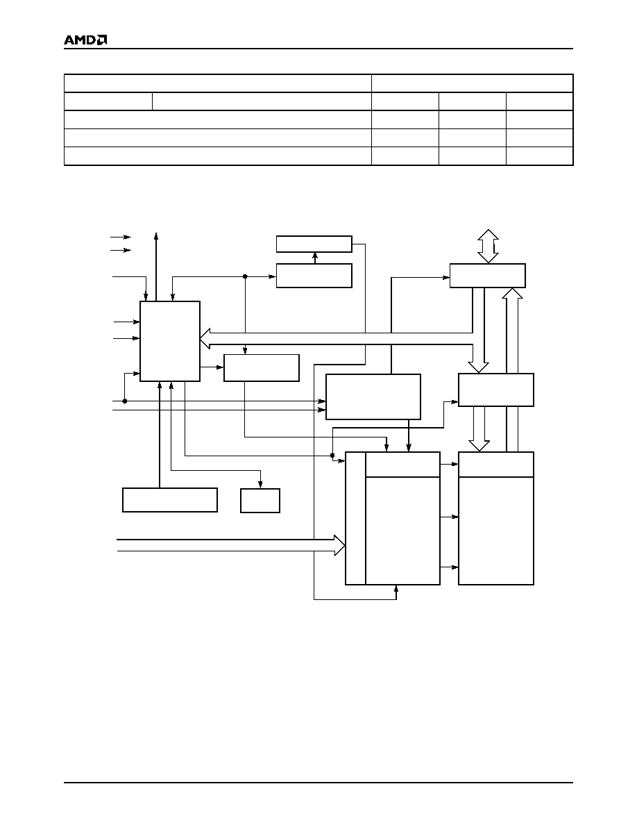
Block Diagram . . . . . . . . . . . . . . . . . . . . . . . . . . . . 4
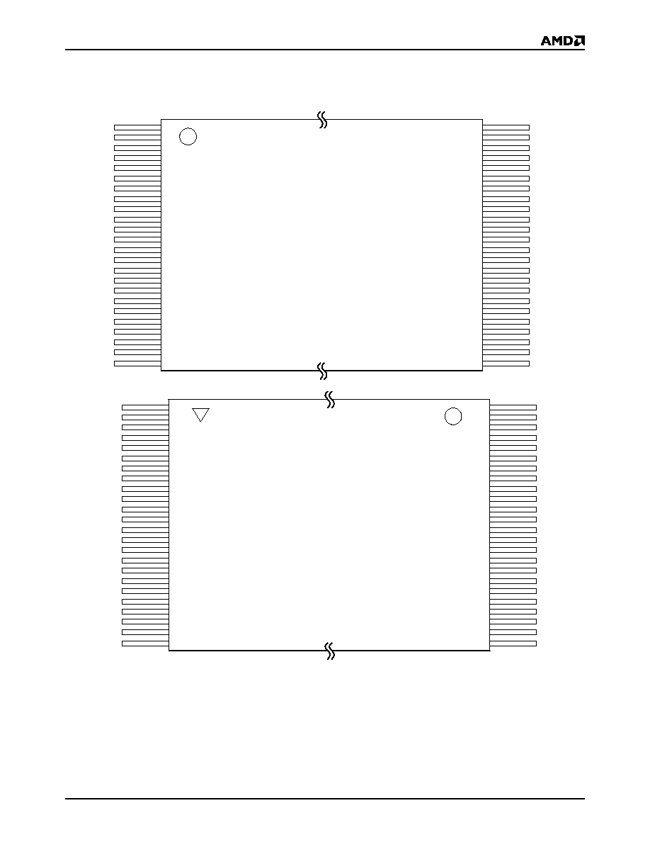
Connection Diagrams . . . . . . . . . . . . . . . . . . . . . . . 5
Special Handling Instructions for FBGA Package .. 7
Pin Configuration . . . . . . . . . . . . . . . . . . . . . . . . . . 7
Logic Symbol . . . . . . . . . . . . . . . . . . . . . . . . . . . . 7
Ordering Information . . . . . . . . . . . . . . . . . . . . . . . 8
Standard Products .................................................. 8
Device Bus Operations . . . . . . . . . . . . . . . . . . . . . . 9
Table 1. Am29LV800B Device Bus Operations ............9
Word/Byte Configuration ........................................ 9
Requirements for Reading Array Data ................... 9
Writing Commands/Command Sequences ............ 9
Program and Erase Operation Status .................. 10
Standby Mode ...................................................... 10
Automatic Sleep Mode ......................................... 10
RESET#: Hardware Reset Pin ............................. 10
Output Disable Mode ............................................ 11
Table 2. Am29LV800BT Top Boot Block
Sector Addresses ........................................................11
Table 3. Am29LV800BB Bottom Boot Block
Sector Addresses ........................................................12
Autoselect Mode ................................................... 12
Table 4. Am29LV800B Autoselect Codes
(High Voltage Method) ................................................13
Sector Protection/Unprotection ............................ 13
Temporary Sector Unprotect ................................ 13
Figure 1. Temporary Sector Unprotect Operation....... 13
Figure 2. In-System Sector Protect/
Sector Unprotect Algorithms ....................................... 14
Hardware Data Protection .................................... 15
Command Definitions . . . . . . . . . . . . . . . . . . . . . 15
Reading Array Data .............................................. 15
Reset Command .................................................. 15
Autoselect Command Sequence .......................... 15
Word/Byte Program Command Sequence ........... 16
Figure 3. Program Operation ...................................... 17
Chip Erase Command Sequence ......................... 17
Sector Erase Command Sequence ...................... 17
Erase Suspend/Erase Resume Commands ......... 18
Figure 4. Erase Operation........................................... 18
Table 5. Am29LV800B Command Definitions .............19
Write Operation Status . . . . . . . . . . . . . . . . . . . . 20
DQ7: Data# Polling ............................................... 20
Figure 5. Data# Polling Algorithm ............................... 20
RY/BY#: Ready/Busy# ......................................... 21
DQ6: Toggle Bit I .................................................. 21
DQ2: Toggle Bit II ................................................. 21
Reading Toggle Bits DQ6/DQ2 ............................ 21
DQ5: Exceeded Timing Limits .............................. 22
DQ3: Sector Erase Timer ..................................... 22
Figure 6. Toggle Bit Algorithm..................................... 22
Table 6. Write Operation Status ..................................23
Absolute Maximum Ratings . . . . . . . . . . . . . . . . . 24
Operating Ranges . . . . . . . . . . . . . . . . . . . . . . . . 24
DC Characteristics . . . . . . . . . . . . . . . . . . . . . . . . 25
CMOS Compatible ............................................... 25
Figure 9. I
CC1
Current vs. Time (Showing Active and
Automatic Sleep Currents) .......................................... 26
Figure 10. Typical I
CC1
vs. Frequency ........................ 26
Test Conditions . . . . . . . . . . . . . . . . . . . . . . . . . . 27
Figure 11. Test Setup.................................................. 27
Table 7. Test Specifications ........................................27
Key to Switching Waveforms. . . . . . . . . . . . . . . . 27
Figure 12. Input Waveforms and
Measurement Levels ................................................... 27
AC Characteristics . . . . . . . . . . . . . . . . . . . . . . . . 28
Read Operations .................................................. 28
Figure 13. Read Operations Timings .......................... 28
Hardware Reset (RESET#) .................................. 29
Figure 14. RESET# Timings........................................ 29
Word/Byte Configuration (BYTE#) ..................... 30
Figure 15. BYTE# Timings for Read Operations......... 30
Figure 16. BYTE# Timings for Write Operations ......... 30
Erase/Program Operations ................................... 31
Figure 17. Program Operation Timings ....................... 32
Figure 18. Chip/Sector Erase Operation Timings........ 33
Figure 19. Data# Polling Timings (During
Embedded Algorithms) ................................................ 34
Figure 20. Toggle Bit Timings (During
Embedded Algorithms) ................................................ 34
Figure 21. DQ2 vs. DQ6.............................................. 35
Temporary Sector Unprotect ................................ 35
Figure 22. Temporary Sector Unprotect
Timing Diagram ........................................................... 35
Figure 23. Sector Protect/Unprotect
Timing Diagram ........................................................... 36
Alternate CE# Controlled
Erase/Program Operations ................................... 37
Figure 24. Alternate CE# Controlled Write
Operation Timings ....................................................... 38
Erase and Programming Performance . . . . . . . 39
Latchup Characteristics . . . . . . . . . . . . . . . . . . . . 39
TSOP and SO Pin Capacitance . . . . . . . . . . . . . . 39
Data Retention. . . . . . . . . . . . . . . . . . . . . . . . . . . . 39
Physical Dimensions . . . . . . . . . . . . . . . . . . . . . . 40
TS 048--48-Pin Standard TSOP ........................ 40
TSR048--48-Pin Reverse TSOP ........................ 41
FBB 048--48-Ball Fine-Pitch Ball Grid Array
(FBGA) 6 x 9 mm ................................................ 42
SO 044--44-Pin Small Outline Package ............. 43
Revision Summary . . . . . . . . . . . . . . . . . . . . . . . . 44
Revision E (January 1998) ................................... 44
Revision E+1 (March 1998) .................................. 44
Revision F (January 1999) ................................... 44
Revision F+1 (February 1999) ............................. 44
Revision F+2 (February 1999) ............................. 44
Revision F+3 (July 2, 1999) ................................. 44
Revision F+4 (July 26, 1999) ............................... 44
Revision G (November 10, 1999) ......................... 45
Revision G+1 (July 7, 2000) ................................. 45
Revision G+2 (August 14, 2000) .......................... 45