
PRELIMINARY
© Copyright 2001 Advanced Micro Devices, Inc. All rights reserved.
Final Draft# 22003
Rev: B Amendment/0
Issue Date: March 2001
…lanTMSC520 Microcontroller
Integrated 32-Bit Microcontroller with PC/AT-Compatible Peripherals,
PCI Host Bridge, and Synchronous DRAM Controller
DISTINCTIVE CHARACTERISTICS
s
Industry-standard Am5
x
86Æ CPU with floating
point unit (FPU) and 16-Kbyte write-back cache
≠ 100-MHz and 133-MHz operating frequencies
≠ Low-voltage operation (core V
CC
= 2.5 V)
≠ 5-V tolerant I/O (3.3-V output levels)
s
E86TM family of x86 embedded processors
≠ Part of a software-compatible family of
microprocessors and microcontrollers well
supported by a wide variety of development tools
s
Integrated PCI host bridge controller leverages
standard peripherals and software
≠ 33 MHz, 32-bit PCI bus Revision 2.2-compliant
≠ High-throughput 132-Mbyte/s peak transfer
≠ Supports up to five external PCI masters
≠ Integrated write-posting and read-buffering for
high-throughput applications
s
Synchronous DRAM (SDRAM) controller
≠ Supports 16-, 64-, 128-, and 256-Mbit SDRAM
≠ Supports 4 banks for a total of 256 Mbytes
≠ Error Correction Code provides system reliability
≠ Buffers improve read and write performance
s
AMDebugTM technology offers a low-cost
solution for the advanced debugging
capabilities required by embedded designers
≠ Allows instruction tracing during execution from
the Am5
x
86 CPU's internal cache
≠ Uses an enhanced JTAG port for low-cost debugging
≠ Parallel debug port for high-speed data exchange
during in-circuit emulation
s
General-Purpose (GP) bus with programmable
timing for 8- and 16-bit devices provides good
performance at low cost
s
ROM/Flash controller for 8-, 16-, and 32-bit devices
s
Enhanced PC/AT-compatible peripherals
provide improved performance
≠ Enhanced programmable interrupt controller
(PIC) prioritizes 22 interrupt levels (up to 15
external sources) with flexible routing
≠ Enhanced DMA controller includes double buffer
chaining, extended address and transfer counts,
and flexible channel routing
≠ Two 16550-compatible UARTs operate at baud
rates up to 1.15 Mbit/s with optional DMA interface
s
Standard PC/AT-compatible peripherals
≠ Programmable interval timer (PIT)
≠ Real-time clock (RTC) with battery backup
capability and 114 bytes of RAM
s
Additional integrated peripherals
≠ Three general-purpose 16-bit timers provide
flexible cascading for 32-bit operation
≠ Watchdog timer guards against runaway software
≠ Software timer
≠ Synchronous serial interface (SSI) offers
full-duplex or half-duplex operation
≠ Flexible address decoding for programmable
memory and I/O mapping and system addressing
configuration
s
32 programmable input/output (PIO) pins
s
Native support for pSOS, QNX, RTXC, VxWorks,
and Windows
Æ
CE operating systems
s
Industry-standard BIOS support
s
Plastic Ball Grid Array (PBGA388) package
GENERAL DESCRIPTION
The …lanTMSC520 microcontroller is a full-featured mi-
crocontroller developed for the general embedded
market. The …lanSC520 microcontroller combines a
32-bit, low-voltage Am5
x
86 CPU with a set of inte-
grated peripherals suitable for both real-time and PC/
AT-compatible embedded applications.
An integrated PCI host bridge, SDRAM controller, enhanced
PC/AT-compatible peripherals, and advanced debugging
features provide the system designer with a wide range of
on-chip resources, allowing support for legacy devices as
well as new devices available in the current PC marketplace.
Designed for medium- to high-performance applications
in the telecommunications, data communications, and
information appliance markets, the …lanSC520 micro-
controller is particularly well suited for applications re-
quiring high throughput combined with low latency. The
compact Plastic Ball Grid Array (PBGA) package pro-
vides a high degree of functionality in a very small form
factor, making it cost-effective for many applications. A
0.25-micron CMOS manufacturing process allows for
low power consumption along with high performance.
2
…lanTMSC520 Microcontroller Data Sheet
P R E L I M I N A R Y
ORDERING INFORMATION
≠100 = 100 MHz
≠133 = 133 MHz
TEMPERATURE RANGE
SPEED OPTION
DEVICE NUMBER/DESCRIPTION
Valid combinations list configurations planned to be
supported in volume for this device. Consult the
local AMD sales office to confirm availability of
specific valid combinations and to check on newly
released combinations.
Valid Combinations
PACKAGE TYPE
A = 388-Pin Plastic Ball Grid Array (PBGA)
…lanSC520 integrated 32-bit microcontroller with
PC/AT-compatible peripherals, PCI host bridge,
and synchronous DRAM controller
≠133
A
C
Valid Combinations
…lanSC520≠100
…lanSC520≠133
AC
…lanSC520
C= Commercial (T
C
=0
C to +85
C)
where: T
C
= case temperature

P R E L I M I N A R Y
…lanTMSC520 Microcontroller Data Sheet
3
TABLE OF CONTENTS
Distinctive Characteristics ............................................................................................................ 1
General Description ..................................................................................................................... 1
Ordering Information .................................................................................................................... 2
Logic Diagram by Interface ........................................................................................................... 6
Logic Diagram by Default Pin Function ........................................................................................ 7
Connection Diagram .................................................................................................................... 8
Pin Designations ........................................................................................................................ 10
Pin Designations (Pin Number) ............................................................................................. 11
Pin Designations (Pin Name) ................................................................................................ 13
Signal Descriptions ..................................................................................................................... 16
Architectural Overview ............................................................................................................... 28
Industry-Standard x86 Architecture ....................................................................................... 30
AMDebugTM Technology for Advanced Debugging .............................................................. 30
Industry-Standard PCI Bus Interface .................................................................................... 30
High-Performance SDRAM Controller ................................................................................. 30
ROM/Flash Controller ........................................................................................................... 30
Flexible Address-Mapping Hardware .................................................................................... 31
Easy-to-Use GP Bus Interface .............................................................................................. 31
Clock Generation .................................................................................................................. 31
Integrated Peripherals ........................................................................................................... 31
JTAG Boundary Scan Test Interface .................................................................................... 32
System Test and Debug Features ........................................................................................ 32
Applications ............................................................................................................................... 33
Clock Generation and Control ................................................................................................... 38
Internal Clocks ...................................................................................................................... 39
Clock Specifications .............................................................................................................. 40
Clock Pin Loading ................................................................................................................. 40
Selecting a Crystal ................................................................................................................ 41
32.768-kHz Crystal Selection ........................................................................................... 41
33-MHz Crystal Selection................................................................................................. 42
Third Overtone Crystal Component Selection .................................................................. 42
Running the …lanTMSC520 Microcontroller at 33.333 MHz ........................................................... 43
Bypassing Internal Oscillators ............................................................................................... 44
RTC Voltage Monitor ................................................................................................................. 45
Backup Battery Considerations ............................................................................................. 46
Using an External RTC Backup Battery ........................................................................... 46
Not Using an External RTC Backup Battery..................................................................... 46
Absolute Maximum Ratings ....................................................................................................... 48
Operating Ranges at Commercial Temperatures ...................................................................... 48
Voltage Levels for Non-PCI Interface Pins ................................................................................ 49
Voltage Levels for PCI Interface Pins ........................................................................................ 49
DC Characteristics Over Commercial Operating Ranges .......................................................... 50
Capacitance ............................................................................................................................... 51
Non-PCI Interface Pin Capacitance ...................................................................................... 51
PCI Interface Pin Capacitance .............................................................................................. 51
Crystal Capacitance .............................................................................................................. 51
Derating Curves .................................................................................................................... 51
Power Characteristics ................................................................................................................ 56
Thermal Characteristics ...................................................................................................................56
388-Pin PBGA Package .............................................................................................................56
Switching Characteristics and Waveforms ................................................................................ 58
Key to Switching Waveforms ................................................................................................ 58

4
…lanTMSC520 Microcontroller Data Sheet
P R E L I M I N A R Y
AC Switching Test Waveforms .................................................................................................. 58
Non-PCI Bus Interface Pins .................................................................................................. 58
PCI Bus Interface Pins .......................................................................................................... 58
Switching Characteristics over Commercial Operating Ranges ....................................................................59
Power-On Reset Timing ........................................................................................................ 59
Reset Timing with Power Applied ......................................................................................... 61
ROM Timing .......................................................................................................................... 63
PCI Bus Timing ..................................................................................................................... 65
SDRAM Timing ..................................................................................................................... 66
SDRAM Clock Timing ........................................................................................................... 68
GP Bus Timing ...................................................................................................................... 69
GP Bus DMA Read Cycle Timing ......................................................................................... 71
GP Bus DMA Write Cycle Timing .......................................................................................... 72
SSI Timing ............................................................................................................................. 73
JTAG Timing ......................................................................................................................... 74
Appendix A: Pin Tables ............................................................................................................ A-1
Pin List Summary Table Column Definitions ............................................................................ A-6
Appendix B: Physical Dimensions ............................................................................................ B-1
388-Pin Plastic BGA (PBGA) Package ................................................................................ B-1
Top View ...................................................................................................................... ........B-1
Bottom View ........................................................................................................................ B-2
Circuit Board Layout Considerations ....................................................................................B-3
Appendix C: Customer Support ................................................................................................C-1
Related Documents ..............................................................................................................C-2
Additional Information ..........................................................................................................C-2
Customer Development Platform .........................................................................................C-2
Third-Party Development Support Products .................................................................................C-2
Customer Service .................................................................................................................C-3
Hotline and World Wide Web Support............................................................................. C-3
Corporate Applications Hotline........................................................................................ C-3
World Wide Web Home Page ......................................................................................... C-3
Documentation and Literature ......................................................................................... C-3
Literature Ordering .......................................................................................................... C-3
Index ................................................................................................................................... Index-1
LIST OF FIGURES
Figure 1.
…lanTMSC520 Microcontroller Block Diagram ....................................................... 29
Figure 2.
…lanTMSC520 Microcontroller-Based Smart Residential Gateway
Reference Design ................................................................................................. 34
Figure 3.
…lanTMSC520 Microcontroller-Based Thin Client Reference Design .................... 35
Figure 4.
…lanTMSC520 Microcontroller-Based Digital Set Top Box Reference Design ....... 36
Figure 5.
…lanTMSC520 Microcontroller-Based Telephone Line Concentrator
Reference Design ................................................................................................. 37
Figure 6.
System Clock Distribution Block Diagram ............................................................. 38
Figure 7.
Clock Source Block Diagram ................................................................................ 39
Figure 8.
32.768-kHz Crystal Circuit .................................................................................... 41
Figure 9.
33.333-MHz Third Overtone Crystal Implementation ............................................ 43
Figure 10.
Bypassing the 32.768-kHz Oscillator .................................................................... 44
Figure 11.
Bypassing the 33-MHz Oscillator .......................................................................... 44
Figure 12.
RTC Voltage Monitor Block Diagram .................................................................... 45
Figure 13.
Circuit with Backup Battery ................................................................................... 47
Figure 14.
Circuit without Backup Battery .............................................................................. 47
Figure 15.
I/O Drive 6-mA Rise Time ..................................................................................... 52

P R E L I M I N A R Y
…lanTMSC520 Microcontroller Data Sheet
5
Figure 16.
I/O Drive 6-mA Fall Time ....................................................................................... 52
Figure 17.
I/O Drive 12-mA Rise Time ................................................................................... 53
Figure 18.
I/O Drive 12-mA Fall Time ..................................................................................... 53
Figure 19.
I/O Drive 24-mA Rise Time ................................................................................... 54
Figure 20.
I/O Drive 24-mA Fall Time ..................................................................................... 54
Figure 21.
PCI Pads Rise Time with 1-ns Rise/Fall ............................................................... 55
Figure 22.
PCI Pads Fall Time with 1-ns Rise/Fall ................................................................. 55
Figure 23.
Thermal Resistance (
C/Watt) .............................................................................. 56
Figure 24.
Thermal Characteristics Equations ....................................................................... 57
Figure 25.
AC Switching Test Waveforms .............................................................................. 58
Figure 26.
Power-Up Timing Sequence ................................................................................. 60
Figure 27.
PWRGOOD Timing for RTC Standalone Mode .................................................... 60
Figure 28.
External System Reset Timing with Power Applied .............................................. 61
Figure 29.
PRGRESET Timing ............................................................................................... 62
Figure 30.
Internal System Reset Timing ............................................................................... 62
Figure 31.
Non-Burst ROM Read Cycle Timing ..................................................................... 64
Figure 32.
Page-Mode ROM Read Cycle Timing ................................................................... 64
Figure 33.
Flash Write Cycle Timing ...................................................................................... 65
Figure 34.
SDRAM Write and Read Timing ........................................................................... 67
Figure 35.
SDRAM Clock Timing ........................................................................................... 68
Figure 36.
GP Bus Non-DMA Cycle Timing ........................................................................... 70
Figure 37.
GP-DMA Read Cycle Timing ................................................................................ 71
Figure 38.
GP-DMA Write Cycle Timing ................................................................................. 72
Figure 39.
SSI Timing ............................................................................................................. 73
Figure 40.
JTAG Boundary Scan Timing ................................................................................ 74
Figure 41.
BGA Ball Pad Layout ........................................................................................... B-3
LIST OF TABLES
Table 1.
Signal Descriptions Table Definitions..................................................................... 16
Table 2.
Signal Descriptions ............................................................................................... 17
Table 3.
Clock Jitter Specifications ..................................................................................... 40
Table 4.
Clock Startup and Lock Times .............................................................................. 40
Table 5.
Oscillator Input Specifications ............................................................................... 40
Table 6.
Analog VCC (VCC_ANLG) Specifications ............................................................ 40
Table 7.
PLL1 Loop Filter Components .............................................................................. 41
Table 8.
Timing Error as It Translates to Clock Accuracy .................................................... 41
Table 9.
32.768-kHz Crystal Specifications ........................................................................ 42
Table 10.
33-MHz Crystal Specifications .............................................................................. 42
Table 11.
RTC Voltage Monitor Component Specifications .................................................. 46
Table 12.
Device Power Dissipation ..................................................................................... 56
Table 13.
VCC_ANLG and VCC_RTC Power Dissipation .................................................... 56
Table 14.
Thermal Resistance (∞C/W)
q
JC
and
q
JA
for BGA Package with 6-Layer Board ... 57
Table 15.
Maximum T
A
for Plastic BGA Package with 6-Layer Board with T
CASE
= 85∞C .... 57
Table 16.
Multiplexed Signal Trade-Offs .............................................................................. A-2
Table 17.
PIOs Sorted by PIO Number ................................................................................ A-4
Table 18.
PIOs Sorted by Signal Name ............................................................................... A-5
Table 19.
Pin List Summary Table Abbreviations ................................................................. A-6
Table 20.
Pin List Summary ................................................................................................. A-7
Table 21.
Related AMD Products--E86TM Family Devices ..................................................C-1
6
…lanTMSC520 Microcontroller Data Sheet
P R E L I M I N A R Y
LOGIC DIAGRAM BY INTERFACE
1
Notes:
1. Pins noted with asterisks are duplicated in this diagram to clarify which signals are used for each interface.
PCI Bus
SDRAM
Serial Ports:
UART 1
UART 2
SSI
AD31≠AD0
CBE3≠CBE0
PAR
SERR
PERR
FRAME
TRDY
IRDY
STOP
DEVSEL
CLKPCIOUT
CLKPCIIN
RST
INTA≠INTD
REQ4≠REQ0
GNT4≠GNT0
BA1≠BA0
MD31≠MD0
SCS3≠SCS0
CLKMEMOUT
CLKMEMIN
SRASA≠SRASB
SCASA≠SCASB
SWEA≠SWEB
SDQM3≠SDQM0
MECC6≠MECC0
SOUT2≠SOUT1
SIN2≠SIN1
RTS2≠RTS1
CTS2≠CTS1
DSR2≠DSR1
DTR2≠DTR1
DCD2≠DCD1
RIN2≠RIN1
SSI_CLK
SSI_DO
SSI_DI
GP Bus
GPA25≠GPA0
GPD15≠GPD0
GPRESET
GPIORD
GPIOWR
GPMEMRD
GPMEMWR
GPALE
GPBHE
GPRDY
GPAEN
GPTC
GPDRQ3≠GPDRQ0
GPDACK3≠GPDACK0
GPIRQ10≠GPIRQ0
GPDBUFOE
GPIOCS16
GPMEMCS16
JTAG
AMDebug
System Test
JTAG_TRST
JTAG_TCK
JTAG_TDI
JTAG_TDO
JTAG_TMS
GPCS7≠GPCS0
BOOTCS
ROMCS2≠ROMCS1
ROMRD
FLASHWR
ROMBUFOE
CMDACK
BR/TC
STOP/TX
TRIG/TRACE
WBMSTR2≠WBMSTR0
CF_DRAM
DATASTRB
CF_ROM_GPCS
PIO31≠PIO0
TMRIN1≠TMRIN0
TMROUT1≠TMROUT0
Programmable
Input/Output
Timers
PITGATE2
PITOUT2
Clocks and Reset
32KXTAL2≠32KXTAL1
33MXTAL2≠33MXTAL1
CLKTIMER
CLKTEST
PWRGOOD
PRGRESET
CFG3≠CFG0
RSTLD7≠RSTLD0
Configuration
DEBUG_ENTER
INST_TRCE
AMDEBUG_DIS
BBATSEN
MD31≠MD0*
GPA25≠GPA0*
GPD15≠GPD0*
ROM/Flash
MA12≠MA0
LF_PLL1
…lanTMSC520 Microcontroller Data Sheet
7
P R E L I M I N A R Y
LOGIC DIAGRAM BY DEFAULT PIN FUNCTION
1
Notes:
1. Pin names in bold indicate the default pin function. Brackets, [ ], indicate alternate, multiplexed functions. Braces, { }, indicate
pinstrap pins. Pins noted with asterisks are duplicated in this diagram to clarify which signals are used for each interface.
PCI Bus
SDRAM
Serial Ports:
UART 1
UART 2
SSI
AD31≠AD0
CBE3≠CBE0
PAR
SERR
PERR
FRAME
TRDY
IRDY
STOP
DEVSEL
CLKPCIOUT
CLKPCIIN
RST
INTA≠INTD
REQ4≠REQ0
GNT4≠GNT0
BA1≠BA0
MD31≠MD0
SCS3≠SCS0
CLKMEMOUT
CLKMEMIN
SRASA≠SRASB
SCASA≠SCASB
SWEA≠SWEB
SDQM3≠SDQM0
MECC6≠MECC0
SOUT2≠SOUT1
SIN2≠SIN1
RTS2≠RTS1
CTS1
DSR1
DTR2≠DTR1
DCD1
RIN1
SSI_CLK
SSI_DO
SSI_DI
GP Bus
ROM/Flash
GPA25 {DEBUG_ENTER}
GPD15≠GPD0
GPRESET
GPIORD
GPIOWR
GPMEMRD
GPMEMWR
PIO0 [GPALE]
PIO1 [GPBHE]
PIO2 [GPRDY]
PIO3 [GPAEN]
PIO4 [GPTC]
PIO5≠PIO8 [GPDRQ3≠GPDRQ0]
PIO9≠PIO12 [GPDACK3≠GPDACK0]
PIO13≠PIO23 [GPIRQ10≠GPIRQ0]
PIO24 [GPDBUFOE]
PIO25 [GPIOCS16]
PIO26 [GPMEMCS16]
JTAG
AMDebug
System Test
JTAG_TRST
JTAG_TCK
JTAG_TDI
JTAG_TDO
JTAG_TMS
PIO27 [GPCS0]
BOOTCS
ROMCS2≠ROMCS1 [GPCS2≠GPCS1]
ROMRD
FLASHWR
ROMBUFOE
CMDACK
BR/TC
STOP/TX
TRIG/TRACE
CF_DRAM [WBMSTR2] {CFG2}
DATASTRB [WBMSTR1] {CFG1}
CF_ROM_GPCS [WBMSTR0] {CFG0}
TMRIN1≠TMRIN0 [GPCS4≠GPCS5]
TMROUT1≠TMROUT0 [GPCS6≠GPCS7]
Timers
PITGATE2 [GPCS3]
PITOUT2 {CFG3}
Clocks and Reset
32MXTAL2≠32MXTAL1
LF_PLL1
CLKTIMER [CLKTEST]
PWRGOOD
PRGRESET
BBATSEN
GPA22≠GPA15 {RSTLD7≠RSTLD0}
GPA13≠GPA0
GPA24 {INST_TRCE}
GPA23 {AMDEBUG_DIS}
PIO28 [CTS2]
PIO29 [DSR2]
PIO30 [DCD2]
PIO31 [RIN2]
MD31≠MD0*
GPA25≠GPA0*
GPD15≠GPD0*
MA12≠MA0
32KXTAL2≠32KXTAL1
8
…lanTMSC520 Microcontroller Data Sheet
P R E L I M I N A R Y
CONNECTION DIAGRAM
388-Pin Plastic BGA Package
Top View
1
2
3
4
5
6
7
8
9
10
11
12
13
A
AD30
AD31
NC
CLKMEMIN RST
CLK-
PCIOUT
CLKTIMER
[CLKTEST]
MD1
MD17
MD3
MD19
MD5
MD21
A
B
AD29
AD28
NC
NC
GPD1
NC
MD0
MD16
MD2
MD18
MD4
MD20
MD6
B
C
GPA6
GPA9
GPA25
{DEBUG_
ENTER}
GPD0
NC
NC
GPD2
GPD3
GPD4
GPD7
GPD8
GPD9
GPD10
C
D
AD26
AD27
GPA23
{AMDEBUG
_DIS}
GPA24
{INST
_TRCE}
VCC_I/O
VCC_I/O
VCC_I/O
VCC_I/O
GPD5
GPD6
VCC_CORE VCC_CORE GPD11
D
E
AD25
AD24
NC
VCC_CORE
E
F
AD23
CBE3
GPA22
{RSTLD7}
VCC_CORE
F
G
AD22
AD21
CLKPCIIN GPA1
G
H
AD19
AD20
INTC
INTD
H
J
AD18
AD17
INTB
VCC_I/O
J
K
CBE2
AD16
INTA
VCC_I/O
K
L
FRAME
IRDY
REQ0
VCC_I/O
GND
GND
GND
L
M DEVSEL
TRDY
GNT0
VCC_I/O
GND
GND
GND
M
N
STOP
PERR
REQ1
GNT1
GND
GND
GND
N
P
PAR
SERR
GNT2
REQ2
GND
GND
GND
P
R
CBE1
AD15
REQ3
VCC_CORE
GND
GND
GND
R
T
AD13
AD14
GNT3
VCC_CORE
GND
GND
GND
T
U
AD12
AD11
REQ4
GNT4
U
V
AD9
AD10
CTS1
DCD1
V
W AD8
CBE0
DTR1
RTS1
W
Y
AD6
AD7
DSR1
VCC_I/O
Y
AA AD5
AD4
RIN1
VCC_I/O
AA
AB AD2
AD3
NC
NC
AB
AC AD1
AD0
NC
PIO25
[GPIOCS16]
VCC_CORE VCC_CORE VCC_CORE PIO12
[GPDACK0]
PIO11
[GPDACK1]
VCC_I/O
VCC_I/O
NC
TRIG/
TRACE
AC
AD NC
NC
PIO31
[RIN2]
PIO26
[GPMEM-
CS16]
PIO24
[GPDBU-
FOE]
PIO19
[GPIRQ4]
PIO18
[GPIRQ5]
PIO13
[GPIRQ10]
PIO10
[GPDACK2]
PIO5
[GPDRQ3]
PIO4
[GPTC]
NC
NC
AD
AE NC
SIN1
PIO30
[DCD2]
PIO27
[GPCS0]
PIO23
[GPIRQ0]
PIO20
[GPIRQ3]
PIO17
[GPIRQ6]
PIO14
[GPIRQ9]
PIO9
[GPDACK3]
PIO6
[GPDRQ2]
PIO3
[GPAEN]
PIO0
[GPALE]
NC
AE
AF NC
SOUT1
PIO29
[DSR2]
PIO28
[CTS2]
PIO22
[GPIRQ1]
PIO21
[GPIRQ2]
PIO16
[GPIRQ7]
PIO15
[GPIRQ8]
PIO8
[GPDRQ0]
PIO7
[GPDRQ1]
PIO2
[GPRDY]
PIO1
[GPBHE]
NC
AF
1
2
3
4
5
6
7
8
9
10
11
12
13
…lanTMSC520 Microcontroller Data Sheet
9
P R E L I M I N A R Y
CONNECTION DIAGRAM (Continued)
388-Pin Plastic BGA Package
Top View
14
15
16
17
18
19
20
21
22
23
24
25
26
A MD7
MD23
MD9
MD25
MD11
MD27
MD28
MD13
MD14
MD30
MD31
GND_ANLG VCC_RTC
A
B MD22
MD8
MD24
MD10
MD26
CLK-
MEMOUT
MD12
MD29
GPA18
{RSTLD3}
MD15
ROMCS1
[GPCS1]
BBATSEN
VCC_ANLG B
C GPA20
{RSTLD5}
GPD13
GPIOWR
GPD14
GPMEMWR GPA21
{RSTLD6}
PWRGOOD GPA19
{RSTLD4}
NC
ROMCS2
[GPCS2]
GPA15
{RSTLD0}
MECC0
MECC4
C
D GPD12
VCC_I/O
VCC_I/O
GPD15
VCC_CORE VCC_CORE PRGRESET VCC_I/O
VCC_I/O
NC
GPA16
{RSTLD1}
MECC5
MECC1
D
E
NC
GPA17
{RSTLD2}
SWEB
SWEA
E
F
GPA7
GPMEMRD SCASA
SCASB
F
G
VCC_CORE GPIORD
SDQM0
SDQM2
G
H
VCC_CORE GPA5
SDQM3
SDQM1
H
J
GPA3
GPA0
SCS2
SCS3
J
K
VCC_I/O
GPA2
SRASA
SRASB
K
L
GND
GND
GND
VCC_I/O
GPA4
MA0
MA1
L
M
GND
GND
GND
GPA10
GPA8
MA3
MA2
M
N
GND
GND
GND
GPA11
GPA12
MA4
MA5
N
P
GND
GND
GND
VCC_CORE GPA13
MA7
MA6
P
R
GND
GND
GND
VCC_CORE GPA14
MA8
MA9
R
T
GND
GND
GND
NC
NC
BA0
MA10
T
U
SOUT2
CMDACK
BA1
MA11
U
V
VCC_I/O
SIN2
SCS0
MA12
V
W
VCC_I/O
CF_DRAM
[WBMSTR2]
{CFG2}
SCS1
MECC2
W
Y
VCC_I/O
PITOUT2
{CFG3}
MECC3
MECC6
Y
AA
VCC_I/O
TMRIN1
[GPCS4]
ROMBUFOE NC
AA
AB
ROMRD
FLASHWR BOOTCS
33MXTAL1 AB
AC VCC_CORE VCC_CORE NC
NC
VCC_I/O
VCC_I/O
TMRIN0
[GPCS5]
PITGATE2
[GPCS3]
GPRESET TMROUT1
[GPCS6]
DATASTRB
[WBMSTR1]
{CFG1}
NC
33MXTAL2 AC
AD NC
NC
NC
NC
NC
SSI_CLK
CF_ROM_
GPCS
[WBMSTR0]
{CFG0}
JTAG_TCK RTS2
TMROUT0
[GPCS7]
BR/TC
NC
NC
AD
AE NC
NC
NC
NC
NC
SSI_DI
NC
JTAG_TMS JTAG_TRST DTR2
NC
NC
32KXTAL2 AE
AF NC
NC
NC
STOP/TX
NC
SSI_DO
NC
JTAG_TDI JTAG_TDO NC
LF_PLL1
NC
32KXTAL1 AF
14
15
16
17
18
19
20
21
22
23
24
25
26

10
…lanTMSC520 Microcontroller Data Sheet
P R E L I M I N A R Y
PIN DESIGNATIONS
This section identifies the pins of the …lanSC520 micro-
controller and lists the signals associated with each
pin.
In all tables the brackets, [ ], indicate alternate, multi-
plexed functions, and braces, { }, indicate reset config-
uration pins (pinstraps). The line over a pin name
indicates an active Low signal. The word pin refers to
the physical wire; the word signal refers to the electrical
signal that flows through it.
s
Pin designations are listed in the "Pin Designations
(Pin Number)" table on page 11 and the Pin
Designations (Pin Name) table on page 13.
s
Table 2, "Signal Descriptions" on page 17 contains
a descr iption of the micro controlle r signals
organized alphabetically by functional group.
Table 1 on page 16 defines terms used in Table 2.
The table includes columns listing the multiplexed
functions and I/O type.
Refer to Appendix A, "Pin Tables," on page A-1 for an
additional group of tables with the following informa-
tion:
s
Multiplexed signal tradeoffs--Table 16 on
page A-2.
s
Programmable I/O pins ordered by 1) PIO pin
n u m b e r a n d 2 ) m u l t i p l e xe d s i g n a l n a m e ,
respectively, including pin numbers, multiplexed
functions, and pin configuration following system
reset--Table 17 on page A-4 and Table 18 on
page A-5.
s
Comprehensive pin and signal summary showing
signal name and alternate function, pin number, I/O
type, maximum load values, power-on reset default
function, reset state, power-on reset default opera-
t i o n , h o l d s t a t e, a n d vo l t a g e -- Ta bl e 2 0 o n
page A-7.
…lanTMSC520 Microcontroller Data Sheet
11
P R E L I M I N A R Y
Pin Designations (Pin Number
1
)
Pin #
Signal Name
Pin #
Signal Name
Pin #
Signal Name
Pin #
Signal Name
Pin #
Signal Name
A1
AD30
B19
CLKMEMOUT
D11
VCC_CORE
H23
VCC_CORE
M23
GPA10
A2
AD31
B20
MD12
D12
VCC_CORE
H24
GPA5
M24
GPA8
A3
NC
B21
MD29
D13
GPD11
H25
SDQM3
M25
MA3
A4
CLKMEMIN
B22
GPA18{RSTLD3}
D14
GPD12
H26
SDQM1
M26
MA2
A5
RST
B23
MD15
D15
VCC_I/O
J1
AD18
N1
STOP
A6
CLKPCIOUT
B24
ROMCS1[GPCS1]
D16
VCC_I/O
J2
AD17
N2
PERR
A7
CLKTIMER
[CLKTEST]
B25
BBATSEN
D17
GPD15
J3
INTB
N3
REQ1
A8
MD1
B26
VCC_ANLG
D18
VCC_CORE
J4
VCC_I/O
N4
GNT1
A9
MD17
C1
GPA6
D19
VCC_CORE
J23
GPA3
N11
GND
A10
MD3
C2
GPA9
D20
PRGRESET
J24
GPA0
N12
GND
A11
MD19
C3
GPA25
{DEBUG_ENTER}
D21
VCC_I/O
J25
SCS2
N13
GND
A12
MD5
C4
GPD0
D22
VCC_I/O
J26
SCS3
N14
GND
A13
MD21
C5
NC
D23
NC
K1
CBE2
N15
GND
A14
MD7
C6
NC
D24
GPA16{RSTLD1}
K2
AD16
N16
GND
A15
MD23
C7
GPD2
D25
MECC5
K3
INTA
N23
GPA11
A16
MD9
C8
GPD3
D26
MECC1
K4
VCC_I/O
N24
GPA12
A17
MD25
C9
GPD4
E1
AD25
K23
VCC_I/O
N25
MA4
A18
MD11
C10
GPD7
E2
AD24
K24
GPA2
N26
MA5
A19
MD27
C11
GPD8
E3
NC
K25
SRASA
P1
PAR
A20
MD28
C12
GPD9
E4
VCC_CORE
K26
SRASB
P2
SERR
A21
MD13
C13
GPD10
E23
NC
L1
FRAME
P3
GNT2
A22
MD14
C14
GPA20{RSTLD5}
E24
GPA17{RSTLD2}
L2
IRDY
P4
REQ2
A23
MD30
C15
GPD13
E25
SWEB
L3
REQ0
P11
GND
A24
MD31
C16
GPIOWR
E26
SWEA
L4
VCC_I/O
P12
GND
A25
GND_ANLG
C17
GPD14
F1
AD23
L11
GND
P13
GND
A26
VCC_RTC
C18
GPMEMWR
F2
CBE3
L12
GND
P14
GND
B1
AD29
C19
GPA21{RSTLD6}
F3
GPA22{RSTLD7}
L13
GND
P15
GND
B2
AD28
C20
PWRGOOD
F4
VCC_CORE
L14
GND
P16
GND
B3
NC
C21
GPA19{RSTLD4}
F23
GPA7
L15
GND
P23
VCC_CORE
B4
NC
C22
NC
F24
GPMEMRD
L16
GND
P24
GPA13
B5
GPD1
C23
ROMCS2[GPCS2]
F25
SCASA
L23
VCC_I/O
P25
MA7
B6
NC
C24
GPA15{RSTLD0}
F26
SCASB
L24
GPA4
P26
MA6
B7
MD0
C25
MECC0
G1
AD22
L25
MA0
R1
CBE1
B8
MD16
C26
MECC4
G2
AD21
L26
MA1
R2
AD15
B9
MD2
D1
AD26
G3
CLKPCIIN
M1
DEVSEL
R3
REQ3
B10
MD18
D2
AD27
G4
GPA1
M2
TRDY
R4
VCC_CORE
B11
MD4
D3
GPA23
{AMDEBUG_DIS}
G23
VCC_CORE
M3
GNT0
R11
GND
B12
MD20
D4
GPA24
{INST_TRCE}
G24
GPIORD
M4
VCC_I/O
R12
GND
B13
MD6
D5
VCC_I/O
G25
SDQM0
M11
GND
R13
GND
B14
MD22
D6
VCC_I/O
G26
SDQM2
M12
GND
R14
GND
B15
MD8
D7
VCC_I/O
H1
AD19
M13
GND
R15
GND
B16
MD24
D8
VCC_I/O
H2
AD20
M14
GND
R16
GND
B17
MD10
D9
GPD5
H3
INTC
M15
GND
R23
VCC_CORE
B18
MD26
D10
GPD6
H4
INTD
M16
GND
R24
GPA14

12
…lanTMSC520 Microcontroller Data Sheet
P R E L I M I N A R Y
R25
MA8
W3
DTR1
AC5
VCC_CORE
AD13
NC
AE21
JTAG_TMS
R26
MA9
W4
RTS1
AC6
VCC_CORE
AD14
NC
AE22
JTAG_TRST
T1
AD13
W23
VCC_I/O
AC7
VCC_CORE
AD15
NC
AE23
DTR2
T2
AD14
W24
CF_DRAM
[WBMSTR2]{CFG2}
AC8
PIO12
[GPDACK0]
AD16
NC
AE24
NC
T3
GNT3
W25
SCS1
AC9
PIO11[GPDACK1]
AD17
NC
AE25
NC
T4
VCC_CORE
W26
MECC2
AC10
VCC_I/O
AD18
NC
AE26
32KXTAL2
T11
GND
Y1
AD6
AC11
VCC_I/O
AD19
SSI_CLK
AF1
NC
T12
GND
Y2
AD7
AC12
NC
AD20
CF_ROM_GPCS
[WBMSTR0]{CFG0}
AF2
SOUT1
T13
GND
Y3
DSR1
AC13
TRIG/TRACE
AD21
JTAG_TCK
AF3
PIO29[DSR2]
T14
GND
Y4
VCC_I/O
AC14
VCC_CORE
AD22
RTS2
AF4
PIO28[CTS2]
T15
GND
Y23
VCC_I/O
AC15
VCC_CORE
AD23
TMROUT0
[GPCS7]
AF5
PIO22[GPIRQ1]
T16
GND
Y24
PITOUT2{CFG3}
AC16
NC
AD24
BR/TC
AF6
PIO21[GPIRQ2]
T23
NC
Y25
MECC3
AC17
NC
AD25
NC
AF7
PIO16[GPIRQ7]
T24
NC
Y26
MECC6
AC18
VCC_I/O
AD26
NC
AF8
PIO15[GPIRQ8]
T25
BA0
AA1
AD5
AC19
VCC_I/O
AE1
NC
AF9
PIO8[GPDRQ0]
T26
MA10
AA2
AD4
AC20
TMRIN0[GPCS5]
AE2
SIN1
AF10
PIO7[GPDRQ1]
U1
AD12
AA3
RIN1
AC21
PITGATE2[GPCS3]
AE3
PIO30[DCD2]
AF11
PIO2[GPRDY]
U2
AD11
AA4
VCC_I/O
AC22
GPRESET
AE4
PIO27[GPCS0]
AF12
PIO1[GPBHE]
U3
REQ4
AA23
VCC_I/O
AC23
TMROUT1[GPCS6]
AE5
PIO23[GPIRQ0]
AF13
NC
U4
GNT4
AA24
TMRIN1[GPCS4]
AC24
DATASTRB
[WBMSTR1]{CFG1}
AE6
PIO20[GPIRQ3]
AF14
NC
U23
SOUT2
AA25
ROMBUFOE
AC25
NC
AE7
PIO17[GPIRQ6]
AF15
NC
U24
CMDACK
AA26
NC
AC26
33MXTAL2
AE8
PIO14[GPIRQ9]
AF16
NC
U25
BA1
AB1
AD2
AD1
NC
AE9
PIO9[GPDACK3]
AF17
STOP/TX
U26
MA11
AB2
AD3
AD2
NC
AE10
PIO6[GPDRQ2]
AF18
NC
V1
AD9
AB3
NC
AD3
PIO31[RIN2]
AE11
PIO3[GPAEN]
AF19
SSI_DO
V2
AD10
AB4
NC
AD4
PIO26
[GPMEMCS16]
AE12
PIO0[GPALE]
AF20
NC
V3
CTS1
AB23
ROMRD
AD5
PIO24[GPDBUFOE]
AE13
NC
AF21
JTAG_TDI
V4
DCD1
AB24
FLASHWR
AD6
PIO19[GPIRQ4]
AE14
NC
AF22
JTAG_TDO
V23
VCC_I/O
AB25
BOOTCS
AD7
PIO18[GPIRQ5]
AE15
NC
AF23
NC
V24
SIN2
AB26
33MXTAL1
AD8
PIO13[GPIRQ10]
AE16
NC
AF24
LF_PLL1
V25
SCS0
AC1
AD1
AD9
PIO10[GPDACK2]
AE17
NC
AF25
NC
V26
MA12
AC2
AD0
AD10
PIO5[GPDRQ3]
AE18
NC
AF26
32KXTAL1
W1
AD8
AC3
NC
AD11
PIO4[GPTC]
AE19
SSI_DI
W2
CBE0
AC4
PIO25 [GPIOCS16]
AD12
NC
AE20
NC
Notes:
1. See Table 17 on page A-4 for PIOs sorted by pin number.
Pin Designations (Pin Number
1
) (Continued)
Pin #
Signal Name
Pin #
Signal Name
Pin #
Signal Name
Pin #
Signal Name
Pin #
Signal Name
…lanTMSC520 Microcontroller Data Sheet
13
P R E L I M I N A R Y
Pin Designations (Pin Name
1
)
Signal Name
Pin #
Signal Name
Pin #
Signal Name
Pin #
Signal Name
Pin #
Signal Name
Pin #
32KXTAL1
AF26
{AMDEBUG_DIS}
GPA23
D3
GND
L11
GND_ANLG
A25
[GPCS1]ROMCS1
B24
32KXTAL2
AE26 BA0
T25
GND
L12
GNT0
M3
[GPCS2]ROMCS2
C23
33MXTAL1
AB26 BA1
U25
GND
L13
GNT1
N4
[GPCS3]PITGATE2
AC21
33MXTAL2
AC26 BBATSEN
B25
GND
L14
GNT2
P3 [GPCS4]TMRIN1
AA24
AD0
AC2
BOOTCS
AB25
GND
L15
GNT3
T3
[GPCS5]TMRIN0
AC20
AD1
AC1
BR/TC
AD24
GND
L16
GNT4
U4
[GPCS6]TMROUT1
AC23
AD2
AB1
CBE0
W2
GND
M11
GPA0
J24
[GPCS7]TMROUT0
AD23
AD3
AB2
CBE1
R1
GND
M12
GPA1
G4
GPD0
C4
AD4
AA2
CBE2
K1
GND
M13
GPA2
K24
GPD1
B5
AD5
AA1
CBE3
F2
GND
M14
GPA3
J23
GPD2
C7
AD6
Y1
CF_DRAM
[WBMSTR2]{CFG2}
W24
GND
M15
GPA4
L24
GPD3
C8
AD7
Y2
CF_ROM_GPCS
[WBMSTR0]{CFG0}
AD20
GND
M16
GPA5
H24
GPD4
C9
AD8
W1
{CFG0}
CF_ROM_GPCS
[WBMSTR0]
AD20
GND
N11
GPA6
C1
GPD5
D9
AD9
V1
{CFG1}DATASTRB
[WBMSTR1]
AC24
GND
N12
GPA7
F23
GPD6
D10
AD10
V2
{CFG2]CF_DRAM
[WBMSTR2}
W24
GND
N13
GPA8
M24
GPD7
C10
AD11
U2
{CFG3}PITOUT2
Y24
GND
N14
GPA9
C2
GPD8
C11
AD12
U1
CLKMEMIN
A4
GND
N15
GPA10
M23
GPD9
C12
AD13
T1
CLKMEMOUT
B19
GND
N16
GPA11
N23
GPD10
C13
AD14
T2
CLKPCIIN
G3
GND
P11
GPA12
N24
GPD11
D13
AD15
R2
CLKPCIOUT
A6
GND
P12
GPA13
P24
GPD12
D14
AD16
K2
CLKTEST
[CLKTIMER]
A7
GND
P13
GPA14
R24
GPD13
C15
AD17
J2
[CLKTIMER]
CLKTEST
A7
GND
P14
GPA15{RSTLD0} C24
GPD14
C17
AD18
J1
CMDACK
U24
GND
P15
GPA16{RSTLD1} D24
GPD15
D17
AD19
H1
CTS1
V3
GND
P16
GPA17{RSTLD2} E24
[GPDACK0]PIO12
AC8
AD20
H2
[CTS2]PIO28
AF4
GND
R11
GPA18{RSTLD3} B22
[GPDACK1]PIO11
AC9
AD21
G2
DATASTRB
[WBMSTR1]{CFG1}
AC24
GND
R12
GPA19{RSTLD4] C21
[GPDACK2]PIO10
AD9
AD22
G1
DCD1
V4
GND
R13
GPA20{RSTLD5} C14
[GPDACK3]PIO9
AE9
AD23
F1
[DCD2]PIO30
AE3
GND
R14
GPA21[RSTLD6} C19
[GPDBUFOE]
PIO24
AD5
AD24
E2
{DEBUG_ENTER}
GPA25
C3
GND
R15
GPA22{RSTLD7} F3
[GPDRQ0]PIO8
AF9
AD25
E1
DEVSEL
M1
GND
R16
GPA23
{AMDEBUG_DIS}
D3
[GPDRQ1]PIO7
AF10
AD26
D1
DSR1
Y3
GND
T11
GPA24
{INST_TRCE]
D4
[GPDRQ2]PIO6
AE10
AD27
D2
[DSR2]PIO29
AF3
GND
T12
GPA25
{DEBUG_ENTER]
C3
[GPDRQ3]PIO5
AD10
AD28
B2
DTR1
W3
GND
T13
[GPAEN]PIO3
AE11
[GPIOCS16]PIO25
AC4
AD29
B1
DTR2
AE23
GND
T14
[GPALE]PIO0
AE12
GPIORD
G24
AD30
A1
FLASHWR
AB24
GND
T15
[GPBHE]PIO1
AF12
GPIOWR
C16
AD31
A2
FRAME
L1
GND
T16
[GPCS0]PIO27
AE4
[GPIRQ0]PIO23
AE5

14
…lanTMSC520 Microcontroller Data Sheet
P R E L I M I N A R Y
[GPIRQ1]PIO22
AF5
MA8
R25
MD31
A24
NC
AE24
PIO12[GPDACK0] AC8
[GPIRQ2]PIO21
AF6
MA9
R26
MECC0
C25
NC
AE25
PIO13[GPIRQ10] AD8
[GPIRQ3]PIO20
AE6
MA10
T26
MECC1
D26 NC
AF1
PIO14[GPIRQ9] AE8
[GPIRQ4]PIO19
AD6
MA11
U26
MECC2
W26 NC
AF13
PIO15[GPIRQ8] AF8
[GPIRQ5]PIO18
AD7
MA12
V26
MECC3
Y25
NC
AF14
PIO16[GPIRQ7] AF7
[GPIRQ6]PIO17
AE7
MD0
B7
MECC4
C26
NC
AF15
PIO17[GPIRQ6] AE7
[GPIRQ7]PIO16
AF7
MD1
A8
MECC5
D25
NC
AF16
PIO18[GPIRQ5] AD7
[GPIRQ8]PIO15
AF8
MD2
B9
MECC6
Y26
NC
AF18
PIO19[GPIRQ4] AD6
[GPIRQ9]PIO14
AE8
MD3
A10
NC
A3
NC
AF20
PIO20[GPIRQ3] AE6
[GPIRQ10]PIO13
AD8
MD4
B11
NC
AA26
NC
AF23
PIO21[GPIRQ2] AF6
[GPMEMCS16]
PIO26
AD4
MD5
A12
NC
AB3
NC
AF25
PIO22[GPIRQ1] AF5
GPMEMRD
F24
MD6
B13
NC
AB4
NC
B3
PIO23[GPIRQ0] AE5
GPMEMWR
C18
MD7
A14
NC
AC3
NC
B4
PIO24
[GPDBUFOE]
AD5
[GPRDY]PIO2
AF11
MD8
B15
NC
AC12
NC
B6
PIO25
[GPIOCS16]
AC4
GPRESET
AC22
MD9
A16
NC
AC16
NC
C5
PIO26
[GPMEMCS16]
AD4
[GPTC]PIO4
AD11
MD10
B17
NC
AC17
NC
C6
PIO27[GPCS0] AE4
{INST_TRCE}
GPA24
D4
MD11
A18
NC
AC25
NC
C22
PIO28[CTS2] AF4
INTA
K3 MD12
B20
NC
AD1
NC
D23
PIO29[DSR2] AF3
INTB
J3
MD13
A21
NC
AD2
NC
E3
PIO30[DCD2] AE3
INTC
H3
MD14
A22
NC
AD12
NC
E23
PIO31[RIN2] AD3
INTD
H4
MD15
B23
NC
AD13
NC
T23
PITGATE2
[GPCS3]
AC21
IRDY
L2
MD16
B8
NC
AD14
NC
T24
PITOUT2{CFG3} Y24
JTAG_TCK
AD21
MD17
A9
NC
AD15
PAR
P1
PRGRESET
D20
JTAG_TDI
AF21
MD18
B10
NC
AD16
PERR
N2
PWRGOOD
C20
JTAG_TDO
AF22
MD19
A11
NC
AD17
PIO0[GPALE] AE12
REQ0
L3
JTAG_TMS
AE21
MD20
B12
NC
AD18
PIO1[GPBHE] AF12
REQ1
N3
JTAG_TRST
AE22
MD21
A13
NC
AD25
PIO2[GPRDY] AF11
REQ2
P4
LF_PLL1
AF24
MD22
B14
NC
AD26 PIO3[GPAEN]
AE11
REQ3
R3
MA0
L25
MD23
A15
NC
AE1
PIO4[GPTC] AD11
REQ4
U3
MA1
L26
MD24
B16
NC
AE13
PIO5[GPDRQ3] AD10
RIN1
AA3
MA2
M26
MD25
A17
NC
AE14
PIO6[GPDRQ2] AE10
[RIN2]PIO31
AD3
MA3
M25
MD26
B18 NC
AE15
PIO7[GPDRQ1] AF10
ROMBUFOE
AA25
MA4
N25
MD27
A19
NC
AE16
PIO8[GPDRQ0] AF9
ROMCS1[GPCS1]
B24
MA5
N26
MD28
A20
NC
AE17
PIO9[GPDACK3]
AE9
ROMCS2
[GPCS2 ]
C23
MA6
P26 MD29
B21
NC
AE18
PIO10[GPDACK2]
AD9
ROMRD
AB23
MA7
P25
MD30
A23
NC
AE20
PIO11[GPDACK1]
AC9
RST
A5
Pin Designations (Pin Name
1
) (Continued)
Signal Name
Pin #
Signal Name
Pin #
Signal Name
Pin #
Signal Name
Pin #
Signal Name
Pin #
…lanTMSC520 Microcontroller Data Sheet
15
P R E L I M I N A R Y
{RSTLD0}GPA15
C24
SDQM1
H26
TMRIN0[GPCS5]
AC20
VCC_CORE
F4
VCC_I/O
D15
{RSTLD1}GPA16
D24
SDQM2
G26
TMRIN1[GPCS4] AA24
VCC_CORE
G23
VCC_I/O
D16
{RSTLD2}GPA17
E24
SDQM3
H25
TMROUT0
[GPCS7]
AD23
VCC_CORE
H23
VCC_I/O
D21
{RSTLD3}GPA18
B22
SERR
P2
TMROUT1
[GPCS6]
AC23
VCC_CORE
P23
VCC_I/O
D22
{RSTLD4}GPA19
C21
SIN1
AE2
TRDY
M2
VCC_CORE
R23
VCC_I/O
J4
{RSTLD5}GPA20
C14
SIN2
V24
TRIG/TRACE
AC13
VCC_CORE
R4
VCC_I/O
K23
{RSTLD6}GPA21
C19
SOUT1
AF2
VCC_ANLG
B26 VCC_CORE
T4
VCC_I/O
K4
{RSTLD7}GPA22
F3
SOUT2
U23
VCC_CORE
AC5
VCC_I/O
AA23
VCC_I/O
L4
RTS1
W4
SRASA
K25
VCC_CORE
AC6
VCC_I/O
AA4
VCC_I/O
L23
RTS2
AD22
SRASB
K26
VCC_CORE
AC7
VCC_I/O
AC10
VCC_I/O
M4
SCASA
F25
SSI_CLK
AD19
VCC_CORE
AC14
VCC_I/O
AC11
VCC_I/O
V23
SCASB
F26
SSI_DI
AE19
VCC_CORE
AC15
VCC_I/O
AC18
VCC_I/O
W23
SCS0
V25
SSI_DO
AF19
VCC_CORE
D11
VCC_I/O
AC19
VCC_I/O
Y4
SCS1
W25
STOP
N1
VCC_CORE
D12
VCC_I/O
D5
VCC_I/O
Y23
SCS2
J25
STOP/TX
AF17
VCC_CORE
D18
VCC_I/O
D6
VCC_RTC
A26
SCS3
J26
SWEA
E26
VCC_CORE
D19
VCC_I/O
D7
[WBMSTR0]{CFG0}
CF_ROM_GPCS
AD20
SDQM0
G25
SWEB
E25
VCC_CORE
E4
VCC_I/O
D8
[WBMSTR1]{CFG1}
DATASTRB
AC24
[WBMSTR2]{CFG2}
CF_DRAM
W24
Notes:
1. See Table 17 on page A-4 for PIOs sorted by pin number.
Pin Designations (Pin Name
1
) (Continued)
Signal Name
Pin #
Signal Name
Pin #
Signal Name
Pin #
Signal Name
Pin #
Signal Name
Pin #

16
…lanTMSC520 Microcontroller Data Sheet
P R E L I M I N A R Y
SIGNAL DESCRIPTIONS
Table 2, "Signal Descriptions" on page 17 contains a
description of the …lanSC520 microcontroller signals.
The microcontroller contains 258 signal pins in addition
to power and ground pins in a Plastic Ball Grid Array
(PBGA) package.
Table 1 describes the terms used in the signal descrip-
tion table. The signals are organized alphabetically
within the following functional groups:
s
Synchronous DRAM (page 17)
s
ROM/Flash (page 18)
s
PCI bus (page 18)
s
GP bus (page 19)
s
Serial ports (page 21)
s
Clocks and reset (page 22)
s
JTAG (page 23)
s
AMDebugTM Interface (page 23)
s
System test (page 23)
s
Chip selects (page 24)
s
Programmable I/O (PIO) (page 25)
s
Timers (page 25)
s
Configuration (page 26)
s
Power (page 27)
Table 1.
Signal Descriptions Table Definitions
Term
Definition
General Terms
[ ]
Indicates the pin alternate function; a pin
defaults to the signal named without the
brackets.
{ }
Indicates the reset configuration pin (pinstrap).
pin
Refers to the physical wire.
signal
Refers to the electrical signal that flows across
a pin.
SIGNAL
A line over a signal name indicates that the
signal is active Low; a signal name without a
line is active High.
Signal Types
Analog
Analog voltage
B
Bidirectional
H
High
I
Input
LS
Programmable to hold last state of pin
O
Totem pole output
O/TS
Totem pole output/three-state output
OD
Open-drain output
OD-O
Open-drain output or totem pole output
Osc
Oscillator
PD
Internal pulldown resistor (~100≠150 k
W)
Power
Power pins
PU
Internal pullup resistor (~100≠150 k
W)
STI
Schmitt trigger input
STI-OD
Schmitt trigger input or open-drain output
TS
Three-state output
…lanTMSC520 Microcontroller Data Sheet
17
P R E L I M I N A R Y
Table 2.
Signal Descriptions
Signal
Multiplexed
Signal
Type
Description
Synchronous DRAM
BA1≠BA0
--
O
Bank Address is the SDRAM bank address bus.
CLKMEMIN
--
I
SDRAM Clock Input is the SDRAM clock return signal used to
minimize skew between the internal SDRAM clock and the
CLKMEMOUT signal provided to the SDRAM devices. This signal
compensates for buffer and load delays introduced by the board design.
CLKMEMOUT
--
O
SDRAM Clock Output is the 66-MHz clock that provides clock
signaling for the synchronous DRAM devices. This clock may require
an external Low skew buffer for system implementations that result in
heavy loading on the SDRAM clock signal.
MA12≠MA0
--
O
SDRAM Address is the SDRAM multiplexed address bus.
MD31≠MD0
--
B
SDRAM Data Bus inputs data during SDRAM read cycles and outputs
data during SDRAM write cycles.
MECC6≠MECC0
--
B
Memory Error Correction Code contains the ECC checksum
(syndrome) bits used to validate and correct data errors.
SCASA≠SCASB
--
O
Column Address Strobes are used in combination with the SRASA≠
SRASB and SWEA≠SWEB to encode the SDRAM command type.
SCASA and SCASB are the same signal provided on two different pins
to reduce the total load connected to CAS.
Suggested system connection:
SCASA for SDRAM banks 0 and 1
SCASB for SDRAM banks 2 and 3
SCS3≠SCS0
--
O
SDRAM Chip Selects are the SDRAM chip-select outputs. These
signals are asserted to select a bank of SDRAM devices. The chip-
select signals enable the SDRAM devices to decode the commands
asserted via SRASA≠SRASB, SCASA≠SCASB, and SWEA≠SWEB.
SDQM3≠SDQM0
--
O
Data Input/Output Masks make SDRAM data output high-impedance
and blocks data input on SDRAM while active. Each of the four
SDQM3≠SDQM0 signals is associated with one byte of four
throughout the array. Each SDQMx signal provides an input mask
signal for write accesses and an output enable signal for read
accesses.
SRASA≠SRASB
--
O
Row Address Strobes are used in combination with the SCASA≠
SCASB and SWEA≠SWEB to encode the SDRAM command type.
SRASA and SRASB are the same signal provided on two different pins
to reduce the total load connected to RAS.
Suggested system connection:
SRASA for SDRAM banks 0 and 1
SRASB for SDRAM banks 2 and 3
SWEA≠SWEB
--
O
SDRAM Memory Write Enables are used in combination with the
SRASA≠SRASB and SCASA≠SCASB to encode the SDRAM
command type.
SWEA and SWEB are the same signal provided on two different pins
to reduce the total load connected to WE.
Suggested system connection:
SWEA for SDRAM banks 0 and 1
SWEB for SDRAM banks 2 and 3

18
…lanTMSC520 Microcontroller Data Sheet
P R E L I M I N A R Y
ROM/Flash
BOOTCS
--
O
ROM/Flash Boot Chip Select is an active Low output that provides
the chip select for the startup ROM and/or the ROM/Flash array (BIOS,
HAL, O/S, etc.). The BOOTCS signal asserts for accesses made to the
64-Kbyte segment that contains the Am5
x
86 CPU boot vector:
addresses 3FF0000h≠3FFFFFFh. In addition to this linear decode
region, BOOTCS asserts in response to accesses to user-
programmable address regions.
FLASHWR
--
O
Flash Write indicates that the current cycle is a write of the selected
Flash device. When this signal is asserted, the selected Flash device
can latch data from the data bus.
GPA25≠GPA0
--
O
General-Purpose Address Bus provides the address to the system's
ROM/Flash devices. It is also the address bus for the GP bus devices.
Twenty-six address lines provide a maximum addressable space of 64
Mbytes for each ROM chip select.
GPD15≠GPD0
--
B
General-Purpose Data Bus inputs data during memory and I/O read
cycles and outputs data during memory and I/O write cycles.
A reset configuration pin (CFG2) allows the GP bus to be used for the
boot chip-select ROM interface. Configuration registers are used to
select whether ROMCS2 and ROMCS1 use the GP bus data bus or
the MD data bus. The GP data bus supports 16-bit or 8-bit ROM
interfaces. Two data buses are selectable to facilitate the use of ROM
in a mixed voltage system.
MD31≠MD0
--
B
Memory Data Bus inputs data during SDRAM read cycles and
outputs data during SDRAM write cycles. Configuration registers are
used to select whether ROMCS2 and ROMCS1 use the GP bus data
bus or the MD data bus. A reset configuration pin (CFG2) allows the
GP data bus to be used for BOOTCS. The memory data bus supports
an 8-, 16-, or 32-bit ROM interface.
ROMBUFOE
--
O
ROM Buffer Output Enable is an optional signal used to enable a
buffer to the ROM/Flash devices if they need to be isolated from the
…lanSC520 microcontroller, other GP bus devices, or SDRAM system
for voltage or loading considerations. This signal asserts for all
accesses through the ROM controller. The buffer direction is controlled
by the ROMRD or FLASHWR signal.
ROMCS2
[GPCS2]
O
ROM/Flash Chip Selects are signals that can be programmed to be
asserted for accesses to user-programmable address regions.
ROMCS1
[GPCS1]
O
ROMRD
--
O
ROM/Flash Read indicates that the current cycle is a read of the
selected ROM/Flash device. When this signal is asserted, the selected
ROM device can drive data onto the data bus.
Peripheral Component Interconnect (PCI) Bus
AD31≠AD0
--
B
PCI Address Data Bus is the PCI time-multiplexed address/data bus.
CBE3≠CBE0
--
B
Command or Byte-Enable Bus functions 1) as a time-multiplexed
bus command that defines the type of transaction on the AD bus,
or 2) as byte enables:
CBE0 for AD7≠AD0
CBE1 for AD15≠AD8
CBE2 for AD23≠AD16
CBE3 for AD31≠AD24
CLKPCIIN
--
I
PCI Bus Clock Input is the 33-MHz PCI bus clock. This pin can be
connected to the CLKPCIOUT pin for systems where the …lanSC520
microcontroller is the source of the PCI bus clock.
Table 2.
Signal Descriptions (Continued)
Signal
Multiplexed
Signal
Type
Description
…lanTMSC520 Microcontroller Data Sheet
19
P R E L I M I N A R Y
CLKPCIOUT
--
O
PCI Bus Clock Output is a 33-MHz clock output for the PCI bus
devices. This signal is derived from the 33MXTAL1/33MXTAL2
interface.
DEVSEL
--
B
Device Select is asserted by the target when it has decoded its
address as the target of the current transaction.
FRAME
--
B
Frame is driven by the transaction initiator to indicate the start and
duration of the transaction.
GNT4≠GNT0
--
O
Bus Grants are asserted by the …lanSC520 microcontroller to grant
access to the bus.
INTA≠INTD
--
I
Interrupt Requests are asserted to request an interrupt. These four
interrupts are the same type of interrupt as the GPIRQ10≠GPIRQ0
signals, and they go to the same interrupt controller. They are named
INTx to match the common PCI interrupt naming convention.
Configuration registers allow inversion of these interrupt requests to
recognize active low interrupt requests. These interrupt requests can
be routed to generate NMI.
IRDY
--
B
Initiator Ready is asserted by the current bus master to indicate that
data is ready on the bus (write) or that the master is ready to accept
data (read).
PAR
--
B
PCI Parity is driven by the initiator or target to indicate parity on the
AD31≠AD0 and CBE3≠CBE0 buses.
PERR
--
B
Parity Error is asserted to indicate a PCI bus data parity error in the
previous clock cycle.
REQ4≠REQ0
--
I
Bus Requests are asserted by the master to request access to the
bus.
RST
--
O
Reset is asserted to reset the PCI devices.
SERR
--
I
System Error is used for reporting address parity errors or any other
system error where the result is catastrophic.
STOP
--
B
Stop is asserted by the target to request that the current bus
transaction be stopped.
TRDY
--
B
Target Ready is asserted by the currently addressed target to indicate
its ability to complete the current data phase of a transaction.
General-Purpose Bus (GP Bus)
GPA14≠GPA0
--
O
General-Purpose Address Bus outputs the physical memory or I/O
port address. Twenty-six address lines provide a maximum
addressable space of 64 Mbytes. This bus also provides the address
to the system's ROM/Flash devices.
GPA15
{RSTLD0}
O{I}
GPA16
{RSTLD1}
O{I}
GPA17
{RSTLD2}
O{I}
GPA18
{RSTLD3}
O{I}
GPA19
{RSTLD4}
O{I}
GPA20
{RSTLD5}
O{I}
GPA21
{RSTLD6}
O{I}
GPA22
{RSTLD7}
O{I}
GPA23
{AMDEBUG_DIS}
O{I}
GPA24
{INST_TRCE}
O{I}
GPA25
{DEBUG_ENTER}
O{I}
Table 2.
Signal Descriptions (Continued)
Signal
Multiplexed
Signal
Type
Description

20
…lanTMSC520 Microcontroller Data Sheet
P R E L I M I N A R Y
[GPAEN]
PIO3
O
GP Bus Address Enable indicates that the current address on the
GPA25≠GPA0 address bus is a memory address, and that the current
cycle is a DMA cycle. All I/O devices should use this signal in decoding
their I/O addresses and should not respond when this signal is
asserted. When GPAEN is asserted, the GPDACKx signals are used
to select the appropriate I/O device for the DMA transfer. GPAEN also
asserts when a DMA cycle is occurring internally.
[GPALE]
PIO0
O
GP Bus Address Latch Enable is driven at the beginning of a GP bus
cycle with valid address. This signal can be used by external devices
to latch the GP address for the current cycle.
[GPBHE]
PIO1
O
GP Bus Byte High Enable is driven active when data is to be
transferred on the upper 8 bits of the GP data bus.
GPD15≠GPD0
--
B
General-Purpose Data Bus inputs data during memory and I/O read
cycles, and outputs data during memory and I/O write cycles.
[GPDACK0]
PIO12
O
GP Bus DMA Acknowledge can each be mapped to one of the seven
available DMA channels. They are asserted active Low to
acknowledge the corresponding DMA requests.
[GPDACK1]
PIO11
O
[GPDACK2]
PIO10
O
[GPDACK3]
PIO9
O
[GPDBUFOE]
PIO24
O
GP Bus Data Bus Buffer Output Enable is used to control the output
enable on an external transceiver that may be on the GP data bus.
Using this transceiver is optional in the system design and is
necessary only to alleviate loading or voltage issues. This pin is
asserted for all external GP bus accesses. It is not asserted during
accesses to the internal peripherals even if GP bus echo mode is
enabled.
Note that if the ROM is configured to use the GP data bus, then its
bytes are not controlled by this buffer enable; they are controlled by the
ROMBUFOE signal.
[GPDRQ0]
PIO8
I
GP Bus DMA Request can each be mapped to one of the seven
available DMA channels. They are asserted active High to request
DMA service.
[GPDRQ1]
PIO7
I
[GPDRQ2]
PIO6
I
[GPDRQ3]
PIO5
I
[GPIOCS16]
PIO25
STI
GP Bus I/O Chip-Select 16 is driven active early in the cycle by the
targeted I/O device on the GP bus to request a 16-bit I/O transfer.
GPIORD
--
O
GP Bus I/O Read indicates that the current cycle is a read of the
currently addressed I/O device on the GP bus. When this signal is
asserted, the selected I/O device can drive data onto the data bus.
GPIOWR
--
O
GP Bus I/O Write indicates that the current cycle is a write of the
currently addressed I/O device on the GP bus. When this signal is
asserted, the selected I/O device can latch data from the data bus.
Table 2.
Signal Descriptions (Continued)
Signal
Multiplexed
Signal
Type
Description
…lanTMSC520 Microcontroller Data Sheet
21
P R E L I M I N A R Y
[GPIRQ0]
PIO23
I
GP Bus Interrupt Request can each be mapped to one of the
available interrupt channels or NMI. They are asserted when a
peripheral requires interrupt service.
Configuration registers allow inversion of these interrupt requests to
recognize active low interrupt requests. These interrupt requests can
be routed to generate NMI.
[GPIRQ1]
PIO22
I
[GPIRQ2]
PIO21
I
[GPIRQ3]
PIO20
I
[GPIRQ4]
PIO19
I
[GPIRQ5]
PIO18
I
[GPIRQ6]
PIO17
I
[GPIRQ7]
PIO16
I
[GPIRQ8]
PIO15
I
[GPIRQ9]
PIO14
I
[GPIRQ10]
PIO13
I
[GPMEMCS16]
PIO26
STI
GP Bus Memory Chip-Select 16 is driven active early in the cycle by
the targeted memory device on the GP bus to request a 16-bit memory
transfer.
[GPMEMRD]
--
O
GP Bus Memory Read indicates that the current GP bus cycle is a
read of the selected memory device. When this signal is asserted, the
selected memory device can drive data onto the data bus.
[GPMEMWR]
--
O
GP Bus Memory Write indicates that the current GP bus cycle is a
write of the selected memory device. When this signal is asserted, the
selected memory device can latch data from the data bus.
[GPRDY]
PIO2
STI
GP Bus Ready can be driven by open-drain devices. When pulled
Low during a GP bus access, wait states are inserted in the current
cycle. This pin has an internal weak pullup that should be
supplemented by a stronger external pullup for faster rise time.
GPRESET
--
O
GP Bus Reset, when asserted, re-initializes to reset state all devices
connected to the GP bus.
[GPTC]
PIO4
O
GP Bus Terminal Count is driven from the internal DMA controller to
indicate that the transfer count for the currently active DMA channel
has reached zero, and that the current DMA cycle is the last transfer.
Serial Ports
CTS1
--
I
Clear To Send is driven back to the serial port to indicate that the
external data carrier equipment (DCE) is ready to accept data.
[CTS2]
PIO28
I
DCD1
--
I
Data Carrier Detect is driven back to the serial port from a piece of
DCE when it has detected a carrier signal from a communications
target.
[DCD2]
PIO30
I
DSR1
--
I
Data Set Ready is used to indicate that the external DCE is ready to
establish a communication link with the internal serial port controller.
[DSR2]
PIO29
I
DTR2≠DTR1
--
O
Data Terminal Ready indicates to the external DCE that the internal
serial port controller is ready to communicate.
RIN1
--
I
Ring Indicate is used by an external modem to inform the serial port
that a ring signal was detected.
[RIN2]
PIO31
I
RTS2≠RTS1
--
O
Request To Send indicates to the external DCE that the internal serial
port controller is ready to send data.
SIN2≠SIN1
--
I
Serial Data In is used to receive the serial data from the external serial
device or DCE into the internal serial port controller.
SOUT2≠SOUT1
--
O
Serial Data Out is used to transmit the serial data from the internal
serial port controller to the external serial device or DCE.
Table 2.
Signal Descriptions (Continued)
Signal
Multiplexed
Signal
Type
Description
22
…lanTMSC520 Microcontroller Data Sheet
P R E L I M I N A R Y
SSI_CLK
--
O
SSI Clock is driven by the …lanSC520 microcontroller SSI port during
active SSI transmit or receive transactions. The idle state of the clock
and the assertion/sample edge are configurable.
SSI_DI
--
STI
SSI Data Input receives incoming data from a peripheral device SSI
port. Data is shifted in on the opposite SSI_CLK signal edge in which
SSI_DO drives data. SSI_DO and SSI_DI can be tied together to
interface to a three-pin SSI peripheral.
SSI_DO
--
OD
SSI Data Output drives data to a peripheral device SSI port. Data is
driven on the opposite SSI_CLK signal edge in which SSI_DI latches
data. The DO signal is normally at high-impedance when no transmit
transaction is active on the SSI port.
Clocks and Reset
32KXTAL2≠
32KXTAL1
--
Osc
32.768-kHz Crystal Interface is used for connecting an external
crystal or oscillator to the …lanSC520 microcontroller. This clock
source is used to clock the real-time clock (RTC). In addition, internal
PLLs generate clocks for the timers and UARTs based on this clock
source.
When an external oscillator is used, 32KXTAL1 should be grounded
and the clock source driven on 32KXTAL2.
33MXTAL2≠
33MXTAL1
--
Osc
33-MHz Crystal Interface is the main system clock for the chip. This
clock source is used to derive the SDRAM, CPU, and PCI clocks.
When an external oscillator is used, 33MXTAL1 should be
unconnected and the clock source driven on 33MXTAL2.
[CLKTEST]
CLKTIMER
O
Test Clock Output is a shared pin that allows many of the internal
clocks to be driven externally. CLKTEST can drive the internal clocks
of the UARTs, PLL1, PLL2, the programmable interval timer (PIT), or
the real-time clock (RTC) for testing or for driving an external device.
CLKTIMER
[CLKTEST]
I
Timer Clock Input is a shared clock pin that can be used to input a
frequency to the programmable interval timer (PIT).
LF_PLL1
--
I
Loop Filter Interface is used for connecting external loop filter
components. Component values and circuit descriptions are
contained in "Clock Generation and Control" on page 38.
PRGRESET
--
STI
Programmable Reset can be programmed to reset the …lanSC520
microcontroller, but allow SDRAM refresh to continue during the reset.
This allows the system to be reset without losing the information stored
in SDRAM.
On power-up, PRGRESET is disabled and must be programmed to be
operational. When disabled, this pin has no effect on the …lanSC520
microcontroller.
PWRGOOD
--
STI
Power Good is a reset signal that indicates to the …lanSC520
microcontroller that the V
CC
levels are within the normal operation
range. It is used to reset the entire chip and must be held Low for one
second after all V
CC
signals (except VCC_RTC) on the chip are High.
This signal must be returned Low before the V
CC
signals degrade to
put the RTC into the correct state for operation in RTC-only mode.
Table 2.
Signal Descriptions (Continued)
Signal
Multiplexed
Signal
Type
Description

…lanTMSC520 Microcontroller Data Sheet
23
P R E L I M I N A R Y
JTAG
JTAG_TCK
--
I
Test Clock is the input clock for test access port.
JTAG_TDI
--
I
Test Data Input is the serial input stream for input data. This pin has
a weak internal pullup resistor. It is sampled on the rising edge of
JTAG_TCK. If not driven, this input is sampled High internally.
JTAG_TDO
--
O/TS
Test Data Output is the serial output stream for result data. It is in the
high-impedance state except when scanning is in progress.
JTAG_TMS
--
I
Test Mode Select is an input for controlling the test access port. This
pin has a weak internal pullup resistor. If it is not driven, it is sampled
High internally.
JTAG_TRST
--
I
JTAG Reset is the test access port (TAP) reset. This pin has a weak
internal pulldown resistor. If not driven, this input is sampled Low
internally and causes the TAP controller logic to remain in the reset
state.
AMDebug Interface
BR/TC
--
I
Break Request/Trace Capture requests entry to AMDebug
technology mode. The AMDebug technology serial/parallel interface
can reconfigure this pin to turn instruction trace capture on or off.
CMDACK
--
O
Command Acknowledge indicates command completion status. It is
asserted High when the in-circuit emulator logic is ready to receive
new commands from the host. It is driven Low when the in-circuit
emulator core is executing a command from the host and remains Low
until the command is completed.
STOP/TX
--
O
Stop/Transmit is asserted High on entry to AMDebug mode. During
normal mode, this is set High when there is data to be transmitted to
the host (during operating system/application communication).
TRIG/TRACE
--
O
Trigger/Trace triggers events to a logic analyzer (optional, from
Am5
x
86 CPU debug registers) or indicates trace on or off status. The
AMDebug technology is used to enable and configure this pin.
System Test
CF_DRAM
[WBMSTR2]
{CFG2}
O{I}
Code Fetch SDRAM, during SDRAM reads, provides code fetch
status. When Low, this indicates that the current SDRAM read is a
CPU code fetch demanded by the CPU, or a read prefetch initiated due
to a demand code fetch by the CPU. When High during reads, this
indicates that the SDRAM read is not a code fetch, and it could have
been initiated by the CPU, PCI master, or the GP bus GP-DMA
controller, either demand or prefetch.
During SDRAM write cycles this pin provides an indication of the
source of the data, either GP-DMA controller/PCI bus master or CPU.
When High, this indicates that either a GP bus DMA initiator or an
external PCI bus master contributed to the current SDRAM write cycle
(the CPU may also have contributed). A Low indicates that the CPU is
the only master that contributed to this write cycle.
CF_ROM_GPCS
[WBMSTR0]
{CFG0}
O{I}
Code Fetch ROM/GPCS provides an indication that the CPU is
performing a code fetch from ROM (on either the GP bus or SDRAM
data bus), or from any GPCSx pin. When Low during a read cycle (as
indicated by either GPMEMRD or ROMRD), the CPU is performing a
code fetch from ROM or a GP bus chip select. At all other times
(including writes), this signal is High.
DATASTRB
[WBMSTR1]
{CFG1}
O{I}
Data Strobe is a debug signal that is asserted to allow the external
system to latch SDRAM data. This can be used to trace data on the
SDRAM interface with an in-circuit emulator probe or logic analyzer.
Table 2.
Signal Descriptions (Continued)
Signal
Multiplexed
Signal
Type
Description
24
…lanTMSC520 Microcontroller Data Sheet
P R E L I M I N A R Y
[WBMSTR0]
CF_ROM_GPCS
{CFG0}
O{I}
Write Buffer Master indicates which block(s) wrote to a rank in the
write buffer (during SDRAM write cycles) and which block is reading
from SDRAM (during SDRAM read cycles).
WBMSTR0, when a logical 1, indicates that the internal GP bus DMA
controller has contributed to the write buffer rank (write cycles) or is
reading from SDRAM (read cycles).
[WBMSTR1]
DATASTRB
{CFG1}
O{I}
WBMSTR1, when a logical 1, indicates that the PCI master has
contributed to the write buffer rank (write cycles) or is reading from
SDRAM (read cycles).
[WBMSTR2]
CF_DRAM
{CFG2}
O{I}
WBMSTR2, when a logical 1, it indicates that the CPU has contributed
to the write buffer rank (write cycles) or is reading from SDRAM (read
cycles).
Chip Selects
[GPCS0]
PIO27
O
General-Purpose Chip Select signals are for the GP bus. They can
be used for either memory or I/O accesses. These chip selects are
asserted for Am5
x
86 CPU accesses to the corresponding regions set
up in the Programmable Address Region (PAR) registers.
[GPCS1]
ROMCS1
O
[GPCS2]
ROMCS2
O
[GPCS3]
PITGATE2
O
[GPCS4]
TMRIN1
O
[GPCS5]
TMRIN0
O
[GPCS6]
TMROUT1
O
[GPCS7]
TMROUT0
O
Table 2.
Signal Descriptions (Continued)
Signal
Multiplexed
Signal
Type
Description
…lanTMSC520 Microcontroller Data Sheet
25
P R E L I M I N A R Y
Programmable I/O (PIO)
PIO0
[GPALE]
B
Programmable Input/Output signals can be programmed as inputs
or outputs. When they are outputs, they can be driven High or Low by
programming bits in registers.
PIO1
[GPBHE]
B
PIO2
[GPRDY]
B
PIO3
[GPAEN]
B
PIO4
[GPTC]
B
PIO5
[GPDRQ3]
B
PIO6
[GPDRQ2]
B
PIO7
[GPDRQ1]
B
PIO8
[GPDRQ0]
B
PIO9
[GPDACK3]
B
PIO10
[GPDACK2]
B
PIO11
[GPDACK1]
B
PIO12
[GPDACK0]
B
PIO13
[GPIRQ10]
B
PIO14
[GPIRQ9]
B
PIO15
[GPIRQ8]
B
PIO16
[GPIRQ7]
B
PIO17
[GPIRQ6]
B
PIO18
[GPIRQ5]
B
PIO19
[GPIRQ4]
B
PIO20
[GPIRQ3]
B
PIO21
[GPIRQ2]
B
PIO22
[GPIRQ1]
B
PIO23
[GPIRQ0]
B
PIO24
[GPDBUFOE]
B
PIO25
[GPIOCS16]
B
PIO26
[GPMEMCS16]
B
PIO27
[GPCS0]
B
PIO28
[CTS2]
B
PIO29
[DSR2]
B
PIO30
[DCD2]
B
PIO31
[RIN2]
B
Timers
PITGATE2
[GPCS3]
I
Programmable Interval Timer 2 Gate provides control for the PIT
Channel 2.
Programmable Interval Timer 2 Output is output from the PIT
Channel 2. This signal is typically used as the PC speaker signal.
PITOUT2
{CFG3}
O{I}
TMRIN0
[GPCS5]
I
Timer Inputs 0 and 1 can be programmed to be the control or clock
for the general-purpose (GP) timers 0 and 1.
TMRIN1
[GPCS4]
I
TMROUT0
[GPCS7]
O
Timer Outputs 0 and 1 are outputs from two of the GP timers. These
outputs can be used as pulse-width modulation signals.
TMROUT1
[GPCS6]
O
Table 2.
Signal Descriptions (Continued)
Signal
Multiplexed
Signal
Type
Description

26
…lanTMSC520 Microcontroller Data Sheet
P R E L I M I N A R Y
Configuration
{AMDEBUG_DIS}
GPA23
I
AMDebug Disable is an active High configuration signal latched at the
assertion of Power Good (PWRGOOD). This pin has a built-in
pulldown resistor.
At Power Good assertion:
Low = Normal operation, mode can be enabled by software.
High = AMDebug mode is disabled and cannot be enabled by software.
{CFG0}
CF_ROM_GPCS
[WBMSTR0]
I
Configuration Inputs 3≠0 are latched into the chip when PWRGOOD
is asserted. These signals are all shared with other features. These
signals have built-in pulldown resistors.
CFG0: Choose 8-, 16-, or 32-bit ROM/Flash interface for BOOTCS.
{CFG1}
DATASTRB
[WBMSTR1]
I
CFG1: Choose 8-, 16-, or 32-bit ROM/Flash interface for BOOTCS.
{CFG2}
CF_DRAM
[WBMSTR2]
I
CFG2: When Low when PWRGOOD is asserted, the …lanSC520
microcontroller uses the GP data bus for BOOTCS. When seen as
High during PWRGOOD assertion, the BOOTCS access is across the
SDRAM data bus. Default is Low (by a built-in pulldown resistor).
{CFG3}
PITOUT2
I
CFG3 (Internal AMD test mode enable):
For normal …lanSC520
microcontroller operation, do not pull High during reset.
{DEBUG_ENTER}
GPA25
I
Enter AMDebug Mode is an active High configuration signal latched
at the assertion of Power Good (PWRGOOD). This pin enables the
AMDebug mode, which causes the processor to fetch and execute
one instruction from the BOOTCS device, and then enter AMDebug
mode where the CPU waits for debug commands to be delivered by
the JTAG port.
This pin has a built-in pulldown resistor.
At PWRGOOD assertion:
High = AMDebug mode enabled
Low = Normal operation
{INST_TRCE}
GPA24
I
Instruction Trace is an active High configuration signal latched at the
assertion of Power Good (PWRGOOD). Enables trace record
generation from Power Good assertion.
This pin has a built-in pulldown resistor.
At PWRGOOD assertion:
High = Trace controller enabled to output trace records
Low = Normal operation
Table 2.
Signal Descriptions (Continued)
Signal
Multiplexed
Signal
Type
Description
CFG1
CFG0
BOOTCS Data Width
0
0
8-bit
0
1
16-bit
1
x (don't care)
32-bit
…lanTMSC520 Microcontroller Data Sheet
27
P R E L I M I N A R Y
{RSTLD0}
GPA15
I
Reset Latched Inputs are shared signals that are latched into a
register when PWRGOOD is asserted. They are used to input static
information to software (i.e., board revision). These signals have built-
in pulldown resistors.
{RSTLD1}
GPA16
I
{RSTLD2}
GPA17
I
{RSTLD3}
GPA18
I
{RSTLD4}
GPA19
I
{RSTLD5}
GPA20
I
{RSTLD6}
GPA21
I
{RSTLD7}
GPA22
I
Power
BBATSEN
--
Analog
Backup Battery Sense is a pin on which real-time clock (RTC)
backup battery voltage is sampled each time PWRGOOD is asserted.
If this pin samples below 2.0 V, the Valid RAM and Time (VRT) bit in
RTC index 0Dh is cleared until read. After the read, the VRT bit is set
until BBATSEN is sensed via a subsequent PWRGOOD assertion.
BBATSEN also provides a power-on-reset signal for the RTC when an
RTC backup battery is applied for the first time.
VCC_ANLG
--
Power
Analog Power Supply for the analog circuits (PLLs).
VCC_CORE
--
Power
Power Supply for the …lanSC520 microcontroller core logic.
VCC_I/O
--
Power
Power Supply to the I/O pad ring.
VCC_RTC
--
Power
Power Supply for the real-time clock and 32-kHz oscillator.
GND --
Power
Digital Ground for the remaining …lanSC520 microcontroller core logic.
GND_ANLG
--
Power
Analog Ground for the analog circuits.
Table 2.
Signal Descriptions (Continued)
Signal
Multiplexed
Signal
Type
Description

28
…lanTMSC520 Microcontroller Data Sheet
P R E L I M I N A R Y
ARCHITECTURAL OVERVIEW
The …lanSC520 microcontroller was designed to provide:
s
A balanced mix of high performance and low-cost
interface mechanisms
s
A high-performance, industry-standard 32-bit PCI bus
s
Glueless interfacing to many 8- and 16-bit I/O pe-
ripherals and an 8- and 16-bit bus with programma-
ble timing
s
A cost-effective system architecture that meets a
wide range of performance criteria while retaining
the lower cost of a 32-bit system
s
A high degree of leverage from present day hard-
ware and software technologies
Figure 1 on page 29 illustrates the integrated Am5
x
86
CPU, bus structure, and on-chip peripherals of the
…lanSC520 microcontroller. Three primary interfaces
are provided:
s
A high-performance, 66-MHz, 32-bit synchronous
DRAM (SDRAM) interface of up to 256 Mbytes is
used for Am5
x
86 CPU code execution, as well as
buffer storage of external PCI bus masters and GP
bus DMA initiators. A high-performance ROM/Flash
interface can also be connected to the SDRAM in-
terface.
s
An industry-standard, 32-bit PCI bus is provided for
high bandwidth I/O peripherals such as local area
network controllers, synchronous communications
controllers, and disk storage controllers.
s
A simple 8/16-bit, 33-MHz general-purpose bus
(GP bus) provides a glueless connection to lower
bandwidth peripherals and NVRAM, SRAM, ROM,
or custom ASICs; supports dynamic bus sizing and
compatibility with many common ISA devices.
These three buses listed above are provided in all op-
erating modes of the …lanSC520 microcontroller.
In addition to these three primary interfaces, the
…lanSC520 microcontroller also contains internal oscil-
lator circuitry and phase locked loop (PLL) circuitry, re-
quiring only two simple crystals for virtually all system
clock generation.
Diagrams showing how the …lanSC520 microcontroller
can be used in various system designs are included in
"Applications" on page 33.
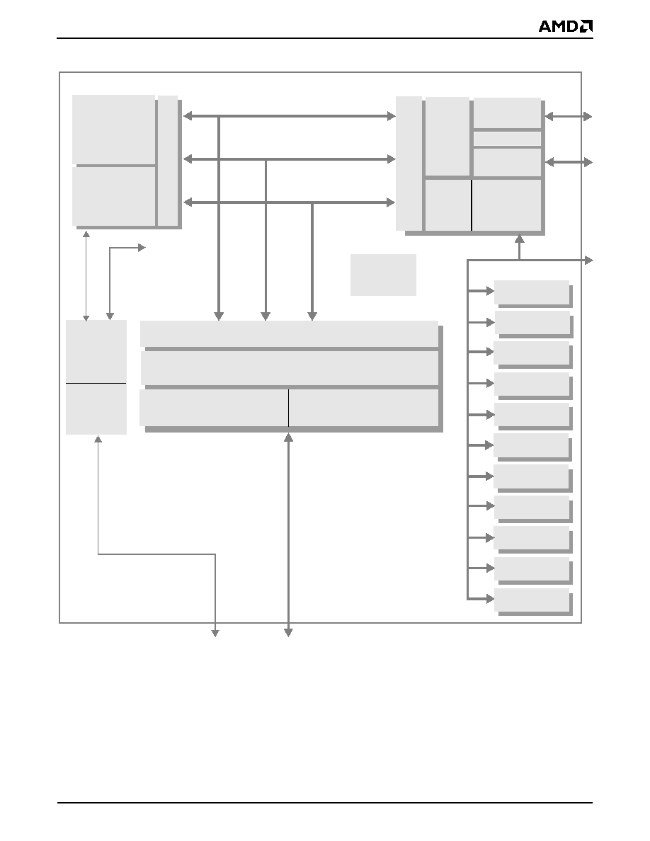
…lanTMSC520 Microcontroller Data Sheet
29
P R E L I M I N A R Y
Figure 1.
…lanTMSC520 Microcontroller Block Diagram
Read/Write Buffers
Address
CPU Bu
s
In
t
e
r
f
a
c
e
Am5
x
86
«
CPU
B
u
s In
ter
f
ac
e Un
i
t
CPU Bus Interface
PCI
Target
PCI
Master
PCI Bus
Arbiter
CPU Bus
Arbiter
Clock
Generation
FIFOs and FIFO
Control
GP-DMA
A
d
dr
es
s
Da
ta
Co
n
t
r
o
l/Sta
t
u
s
CPU Data Bus
CPU Address Bus
CPU Control/Status Bus
GP Bus
AMDebugTM
Technology and
JTAG
Request and
Grant
PCI Bus
PCI Requests and Grants
GP Bus
Controller
ROM/Flash
Controller
SDRAM
Controller
CPU
R
e
q
ues
t
External GP Bus
GP-DMA
Controller
…lanTMSC520 Microcontroller
Programmable
Interrupt Controller
Programmable
Interval Timer
Watchdog Timer
Real-Time Clock
CMOS RAM
General-Purpose
Timers
Software
Timer
16550 UART
16550 UART
Synchronous Serial
Interface
Programmable I/O
Controls
PC/AT Compatibility
Logic
Decode
Unit
Read/Write Buffers

30
…lanTMSC520 Microcontroller Data Sheet
P R E L I M I N A R Y
Industry-Standard x86 Architecture
The Am5
x
86 CPU in the …lanSC520 microcontroller
utilizes the industry-standard x86 microprocessor in-
struction set that enables compatibility across a variety
of performance levels from the 16-bit Am186TM proces-
sors to the high-end AMD AthlonTM processor. Soft-
wa re wr itten for th e x86 architectu re family is
compatible with the …lanSC520 microcontroller.
Other benefits of the Am5
x
86 CPU include:
s
Improved time-to-market and easy software migra-
tion
s
Existing availability of multiple operating systems
that directly support the x86 architecture. Whether
the application requires a real-time operating sys-
tem (RTOS) or one of the popular Microsoft
Æ
oper-
ating systems, the …lanSC520 microcontroller
provides consistent compatibility with many off-the-
shelf operating systems.
s
Multiple sources of field-proven development tools
s
Integrated floating point unit (FPU) (compliant with
ANSI/IEEE 754 standard)
s
16-KByte unified cache configurable for either write-
back or write-through cache mode
AMDebugTM Technology for Advanced
Debugging
The …lanSC520 microcontroller provides support for
low-cost, full-featured, in-circuit emulation capability.
This in-circuit emulation support was developed at
AMD specifically to enable users to test and debug
their software earlier in the design cycle. Utilizing this
capability, the software can be more extensively exer-
cised, and at full execution speeds. It also allows trac-
ing during execution from the Am5
x
86 CPU's internal
cache.
AMDebug technology provides the product design
team with two different communication paths on the
…lanSC520 microcontroller, each of which is supported
by powerful debug tools from third-party vendors in
AMD's FusionE86
SM
program.
s
Serial AMDebug technology uses a serial connec-
tion based on an enhanced JTAG protocol and an
inexpensive 12-pin connector that can be placed on
each board design. This low-cost solution satisfies
the requirement of a large number of software de-
velopers.
s
Parallel AMDebug technology uses a parallel debug
port to exchange commands and data between the
…lanSC520 microcontroller and the host. The
higher pin count requires that the extra signal pins
be provided on a special bond-out package of the
…lanSC520 microcontroller, which is only made
available to tool developers such as in-circuit emu-
lator manufacturers. The parallel AMDebug port
greatly simplifies the task of supporting high speed
data exchange.
Industry-Standard PCI Bus Interface
The …lanSC520 microcontroller provides a 33-MHz,
32-bit PCI bus Revision 2.2-compliant host bridge in-
terface, including integrated write-posting and read-
buffering capabilities suitable for high-throughput appli-
cations. The PCI host bridge leverages standard pe-
ripherals and software. It also provides:
s
High throughput (132 Mbytes/s peak transfer rate)
s
Deep buffering and support for burst transactions
from PCI bus masters to SDRAM
s
Flexible arbitration mechanism
s
Support for up to five external PCI masters
High-Performance SDRAM Controller
The …lanSC520 microcontroller provides an integrated
SDRAM controller that supports popular industry-stan-
dard synchronous DRAMs (SDRAM).
s
The SDRAM controller interfaces with SDRAM
chips as well as with most standard DIMMs to en-
able use of standard off-the-shelf memory compo-
nents.
s
The SDRAM controller supports programmable tim-
ing options and provides the required external
clock.
s
Up to four 32-bit banks of SDRAM are supported
with a maximum capacity of 256 Mbytes.
s
An important reliability-enhancing Error Correction
Code (ECC) feature is built into the SDRAM control-
ler. The resultant increase in the memory content
reliability enables the …lanSC520 microcontroller to
be effectively utilized in applications that require
more reliable operation, such as communications
environments.
s
The SDRAM controller contains a write buffer and
read ahead buffer subsystem that improves both
write and read performance.
s
SDRAM refresh options allow the SDRAM contents
to be maintained during reset.
ROM/Flash Controller
The …lanSC520 microcontroller provides an integrated
ROM controller for glueless interfacing to ROM and
Flash devices. The …lanSC520 microcontroller sup-
ports two types of interfaces to such devices--a simple
interface via the GP bus (see "Easy-to-Use GP Bus In-
terface" on page 31) for 8- and 16-bit devices, and an
interface to the SDRAM memory data bus for higher
performance 8-, 16-, and 32-bit devices.

…lanTMSC520 Microcontroller Data Sheet
31
P R E L I M I N A R Y
The ROM/Flash controller:
s
Reduces system cost by gluelessly interfacing
static memory with up to three ROM/Flash chip se-
lects
s
Supports execute-in-place (XIP) operating systems
for applications that require executing out of ROM or
Flash memory instead of DRAM
s
Supports high-performance page-mode devices
Flexible Address-Mapping Hardware
In addition to the memory management unit (MMU)
within the Am5
x
86 CPU core, the …lanSC520 micro-
controller provides 16 Programmable Address Region
(PAR) registers that enable flexible placement of mem-
ory (SDRAM, ROM, Flash, SRAM, etc.) and peripher-
als into the two address spaces of the Am5
x
86 CPU
(memory address space and I/O address space). The
PAR hardware allows designers to flexibly configure
both address spaces and place memory and/or exter-
nal peripherals, as required by the application. The in-
ternal memory-mapped configuration registers space
can also be remapped to accommodate system re-
quirements. PAR registers also allow control of impor-
tant attributes, such as cacheability, write protection,
and code execution protection for memory resources.
Easy-to-Use GP Bus Interface
The …lanSC520 microcontroller includes a simple gen-
eral-purpose bus (GP bus) that provides programma-
ble bus timing and allows the connection of 8/16-bit
peripheral devices and memory to the …lanSC520 mi-
crocontroller. The GP bus operates at 33 MHz, which
offers good performance at a very low interface cost.
The …lanSC520 microcontroller provides up to eight
chip selects for external GP bus devices such as off-
the-shelf I/O peripherals, custom ASICs, and SRAM or
NVRAM. The GP bus interface supports programma-
ble timing and dynamic bus width and cycle stretching
to accommodate a wide variety of standard peripher-
als, such as UARTs, 10-Mbit LAN controller chips and
serial communications controllers. Up to four external
DMA channels provide fly-by DMA transfers between
peripheral devices on the GP bus and system SDRAM.
Internally, the GP bus is used to provide a complement
of integrated peripherals, such as a DMA controller,
programmable interrupt controller, timers, and UARTs,
as described in "Integrated Peripherals" on page 31.
These internal peripherals are designed to operate at
the full clock rate of the GP bus. The internal peripher-
als can also be configured to operate in PC/AT-compat-
ible configuration, but are generally not restricted to
this configuration.
The …lanSC520 microcontroller provides a way to view
accesses to the internal peripherals on the external GP
bus for debugging purposes.
Clock Generation
The …lanSC520 microcontroller offers user-config-
urable CPU core clock speed operation at 100 or 133
MHz for different power/performance points depending
on the application.
Not all …lanSC520 microcontroller devices support all
CPU clock rates. The maximum supported clock rate
for a device is indicated by the part number printed on
the package. The clocking circuitry can be pro-
grammed to run the device at higher than the rated
speeds. However, if an …lanSC520 microcontroller is
programmed to run at a higher clock speed than that for
which it is rated, then erroneous operation can result,
and physical damage to the device may occur.
The …lanSC520 microcontroller includes on-chip oscilla-
tors and PLLs, as well as most of the required PLL loop
filter components. The …lanSC520 microcontroller re-
quires two standard crystals, one for 32.768 kHz and
one for 33 MHz. All the clocks required inside the
…lanSC520 microcontroller are generated from these
crystals. The …lanSC520 microcontroller also supplies
the clocks for the SDRAM and PCI bus; however, exter-
nal clock buffering may be required in some systems.
Note: The …lanSC520 microcontroller supports either
a 33.000-MHz or 33.333-MHz crystal. In this docu-
ment, the generic term "33 MHz" refers to the system
clock derived from whichever 33-MHz crystal fre-
quency is being used in the system.
Integrated Peripherals
The …lanSC520 microcontroller is a highly integrated
single-chip CPU with a set of integrated peripherals
that are a superset of common PC/AT peripherals, plus
a set of memory-mapped peripherals that enhance its
usability in various applications.
s
A programmable interrupt controller (PIC) that pro-
vides the capability to prioritize 22 interrupt levels,
up to 15 of these being external sources. The PIC
can be programmed to operate in PC/AT-compati-
ble mode, but also contains extended features, in-
cluding support for more sources and flexible
routing that allows any interrupt request to be
steered to any PIC input. Interrupt requests can be
programmed to generate either non-maskable in-
terrupt (NMI) or maskable interrupt requests.
s
An integrated DMA controller is included for trans-
ferring data between SDRAM and GP bus peripher-
als. The GP-DMA controller operates in single-cycle
(fly-by) mode for more efficient transfers. The GP-
DMA controller can be programmed for PC/AT com-
patibility, but also contains enhanced features:
≠ A double buffer-chaining mode provides a more
efficient software interface
≠ Extended address and transfer counts
≠ Flexible routing of DMA channels

32
…lanTMSC520 Microcontroller Data Sheet
P R E L I M I N A R Y
s
Three general-purpose 16-bit timers that provide
flexible cascading for extension to 32-bit operation.
These timers provide the ability to configure down
to the resolution of four clock periods where the
clock period is the 33-MHz clock. Timer input and
output pins provide the ability to interface with off-
chip hardware.
s
A standard PC/AT-compatible programmable inter-
val timer (PIT) that consists of three 16-bit timers.
s
A software timer that eases the task of keeping sys-
tem time. It provides 1-
m
s resolution and can also
be used for performance monitoring.
s
A watchdog timer to guard against runaway soft-
ware.
s
A real-time clock (RTC) with battery backup capa-
bility. The RTC also provides 114 bytes of battery-
backed RAM for storage of configuration parame-
ters.
s
Two integrated 16550-compatible UARTs that pro-
vide full handshaking capability with eight pins
each. Enhancements enable the UARTs to operate
at baud rates up to 1.152 Mbits/s. The UARTs can
be configured to use the integrated GP bus DMA
controller to transfer data between the serial ports
and SDRAM.
s
A synchronous serial interface (SSI) that is compat-
ible with SCP, SPI, and Microwire slave devices.
The SSI interface can be configured for either full-
duplex or half-duplex operation using a 4-wire or
3-wire interface.
s
32 programmable I/O pins are provided. These pins
are multiplexed with other peripherals and interface
functions.
s
The …lanSC520 microcontroller also provides PC/
AT-compatible functions for control of the a20 gate
and the soft CPU reset (Por ts 0060h, 0064h,
0092h).
JTAG Boundary Scan Test Interface
The …lanSC520 microcontroller provides a JTAG test
port that is compliant with IEEE 1149.1 for use during
board testing.
System Test and Debug Features
To facilitate debugging, the …lanSC520 microcontroller
provides observability of many portions of its internal
operation, including:
s
A three-pin interface that can be used in either sys-
tem test mode or write buffer test mode, to aid in de-
termining internal bus initiators of SDRAM cycles,
and determining when SDRAM data is valid on the
interface. An additional mode provides observability
of integrated peripheral accesses.
s
A nonconcurrent arbitration mode to reduce debug
complexity when PCI bus masters and GP bus
DMA initiators are also accessing SDRAM.
s
CPU cache control and dynamic core clock speed
control under program control.
s
Ability to disable write posting and read prefetching
in the SDRAM controller to simplify tracing of
SDRAM cycles.
s
Notification of memory write protection and non-ex-
ecutable memory region violations.

…lanTMSC520 Microcontroller Data Sheet
33
P R E L I M I N A R Y
APPLICATIONS
T h e f ig u r e s o n t h e fo l low i n g p a g e s s h ow t h e
…lanSC520 microcontroller as it might be used in sev-
eral reference design applications in the data commu-
n i c a t i o n s , i n f o r m a t i o n a p p l i a n c e s , a n d
telecommunication markets.
s
Figure 2 on page 34 shows an …lanSC520 micro-
controller-based Smart Resident Gateway (SRG),
which is a router for a home network between the
wide area network (WAN) (the internet) and a local
area network (LAN) (an intranet of computers and
information appliances in the home). The SRG pro-
vides firewall protection of the LAN from unautho-
rized access through the internet. A common
internet access medium is shared by all users on
the LAN.
A variety of connections are possible for both the
WAN and the LAN. For example, the WAN connec-
tion can be a V.90 modem, cable modem, ISDN,
ADSL, or Ethernet.
The LAN connection can be:
≠ HomePNA--Home Phoneline Networking Alli-
ance, an alliance with a widely endorsed home
networking specification;
≠ Bluetooth--a computing and telecommunica-
tions industry specification that describes how
computing devices can easily interconnect with
each other and with home and business phones
and computers using a short-range wireless con-
nection);
≠ Home RF--a standard competing with Bluetooth
for the interconnection of computing devices in a
LAN using radio frequency;
≠ Ethernet--local area network technology;
≠ power line--a LAN using the AC power distribu-
tion network in a home or business to intercon-
nect devices. Digital information is transmitted on
a high-frequency carrier signal on top of the AC
power.
s
Figure 3 on page 35 shows an …lanSC520 micro-
controller-based "thin client," which is the modern
replacement for the traditional terminal in a remote
computing paradigm. Application programs run re-
motely on a server, and data is warehoused on cen-
trally managed disks at the "server farm." An
efficient communications protocol transmits key-
board and mouse commands upstream and trans-
mits video BIOS calls downstream. The thin client
renders and displays the graphics for the user.
The thin client is typically connected to an Ethernet
LAN, although a remote location can connect to a
server via a WAN connection such as a modem. A
minimum speed of 24 kbaud is required for the com-
munication protocol, unless the application is graph-
ics-intensive, in which case a faster connection is
required.
s
Figure 4 on page 36 shows an …lanSC520 micro-
controller-based digital set top box (DSTB), which is
a consumer client device that uses a television set
as the display. Common applications for the DSTB
are internet access, e-mail, and streaming audio
and video content.
The minimal system includes a connection to the
WAN via a modem, ADSL, or cable modem; an out-
put to a TV; and an InfraRed (IR) link to a remote
control or wireless keyboard. Expanded systems in-
clude DVD drives and MPEG2 decoders to deliver
digital video content. A hard drive may be employed
to store video data for future replay. Keyboard,
mouse, printer, or a video camera are options that
can be included.
s
Figure 5 on page 37 shows an …lanSC520 micro-
controller-based telephone line concentrator lo-
cated in the neighborhood that converts multiple
analog subscriber loops into a high-speed digitally
multiplexed line for connection to the central office
switching network.
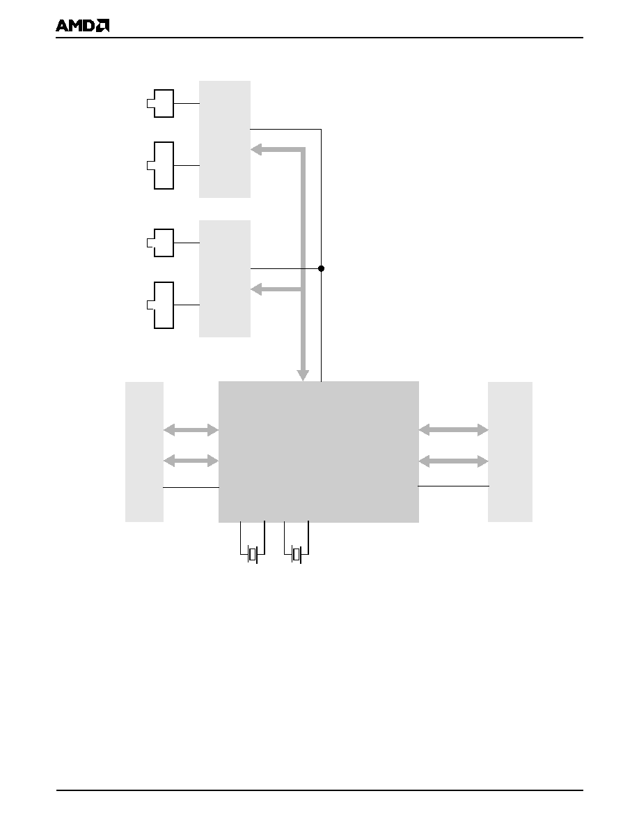
34
…lanTMSC520 Microcontroller Data Sheet
P R E L I M I N A R Y
…lanTMSC520 Microcontroller
GP Bus
GPA25≠GPA0
GPD15≠GPD0
Control
MA12≠MA0
MD31≠MD0
Control
SDRAM
AD
3
1≠AD
0
C
ont
rol
PCne
tTM-Hom
e
W
AN Inte
r
f
a
c
e
A
m
79
C
9
78
3
2
-
kHz Cr
y
s
t
a
l
F
l
as
h o
r
R
O
M
PCI Bus
SDRAM
Bus
AD
SL, C
a
ble
M
ode
m
LAN Inte
r
face
R
J
-45
33-M
H
z
C
r
ys
tal
RJ
-11
or
V
.
9
0
Figure 2.
…lanTMSC520 Microcontroller-Based Smart Residential Gateway Reference Design
or
RJ
-45
RJ
-11
or
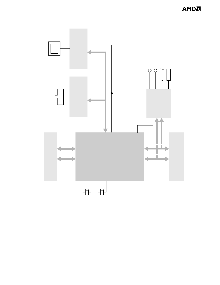
…lanTMSC520 Microcontroller Data Sheet
35
P R E L I M I N A R Y
AD31≠
AD0
Co
ntro
l
…lanTMSC520 Microcontroller
GP Bus
Control
C
o
nt
r
o
ll
e
r
VGA/L
C
D
Fla
s
h
PCI Bus
SDRAM
Bu
s
Am
79
C
9
73
/Am7
9C
97
5
PCnetTM
-
Fas
t
III
Sup
e
r I/
O
PS/2 Key
boa
rd
PS/2 Mo
us
e
Para
lle
l
Seri
al
CRT/L
CD
MA12≠MA0
MD31≠MD0
Control
SDRAM
Control
3
2
-k
Hz Crys
ta
l
3
3
-M
Hz Crys
ta
l
RJ
-
4
5
LAN Inte
r
face
Figure 3.
…lanTMSC520 Microcontroller-Based Thin Client Reference Design
Me
mo
r
y
GPD15≠GPD0
GPA25≠GPA0
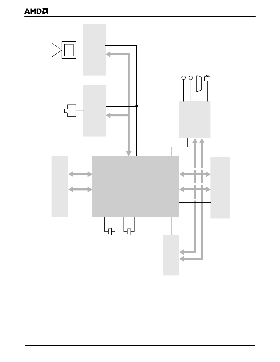
36
…lanTMSC520 Microcontroller Data Sheet
P R E L I M I N A R Y
Fl
a
s
h
…lanTMSC520 Microcontroller
GP Bus
PCI Bus
SDRAM
B
u
s
EIDE
DV
D
o
r
H
D
D
C
ont
rol
GPA1
≠GPA0
G
P
D
15≠
GPD
0
MA12≠MA0
MD31≠MD0
Control
SDRAM
AD
3
1≠AD
0
Con
t
rol
N
T
SC/PAL
VG
A
Supe
r I/O
P
S
/2 Ke
yb
oard
P
S
/2 M
o
u
s
e
Pa
r
a
ll
e
l
IR
C
ontro
l
32-
kH
z
C
r
ys
tal
33-M
H
z
C
r
ys
tal
WAN Inte
r
fa
c
e
AD
SL,
C
a
bl
e M
ode
m
or
V
.
90
RJ
-1
1
Figure 4.
…lanTMSC520 Microcontroller-Based Digital Set Top Box Reference Design
Me
mo
r
y
GPA25≠GPA0
GPD15≠GPD0
Control
…lanTMSC520 Microcontroller Data Sheet
37
P R E L I M I N A R Y
…lanTMSC520 Microcontroller
GP Bu
s
SDRAM
Bus
HDL
C
PCM Highway
T1
or E1
(6x
to
10X)
3
2
-k
Hz Cry
s
ta
l
3
3
-M
Hz Cry
s
ta
l
MA12≠MA0
MD31≠MD0
Control
SDR
A
M
Control
Fl
a
s
h
Co
ntro
l
Figure 5.
…lanTMSC520 Microcontroller-Based Telephone Line Concentrator Reference Design
Me
mo
r
y
IS
L
I
C
Am
79R
2
4
1
Q
u
ad I
S
LAC
Am
79
Q
224
1
IS
L
I
C
Am
79R
2
4
1
IS
L
I
C
Am
79R
2
4
1
IS
L
I
C
Am
79R
2
4
1
IS
L
I
C
Am
79R
2
4
1
Q
u
ad I
S
LAC
Am
79
Q
224
1
IS
L
I
C
Am
79R
2
4
1
IS
L
I
C
Am
79R
2
4
1
IS
L
I
C
Am
79R
2
4
1
T1
/
E
1
In
terfa
c
e
SSI
Anal
og
Phon
e
Lin
e
s
GPD15≠GPD0
GPA25≠GPA0
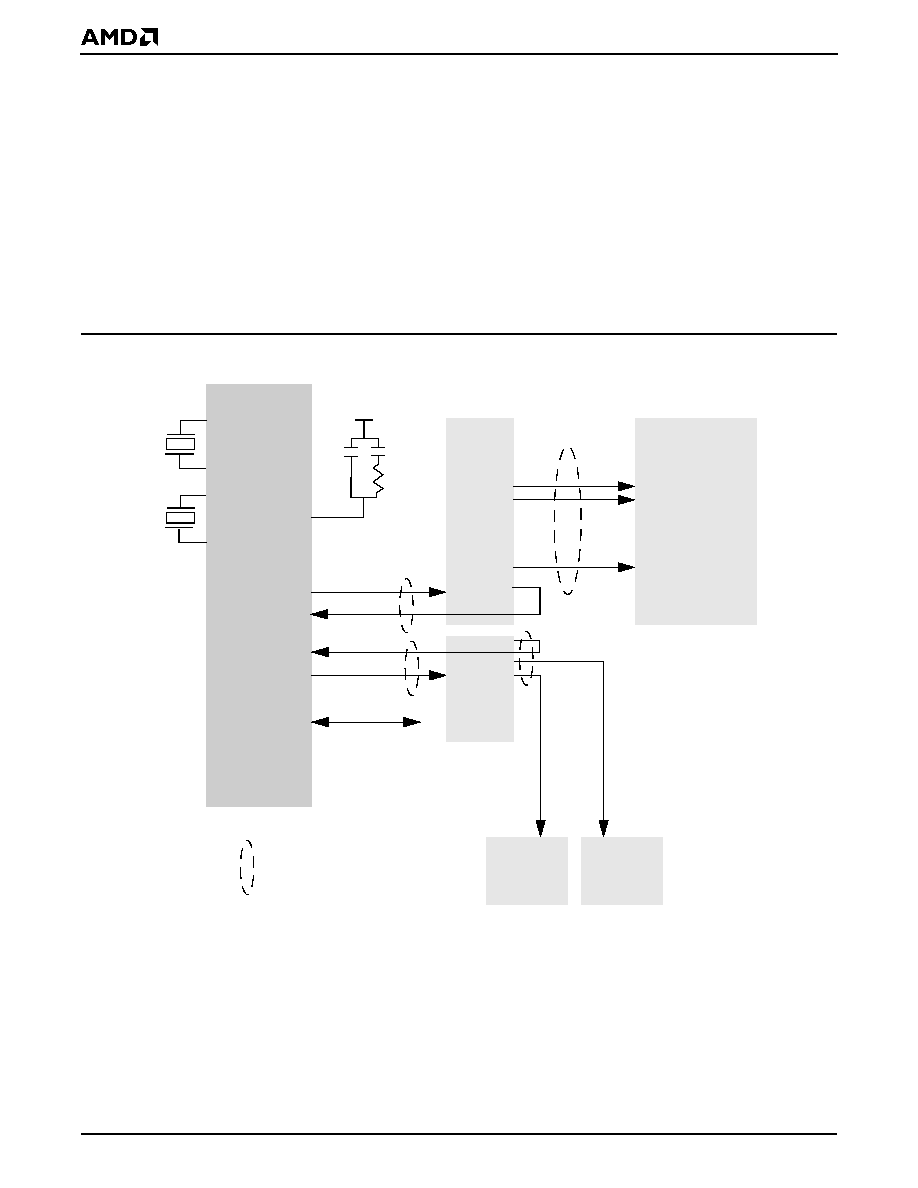
38
…lanTMSC520 Microcontroller Data Sheet
P R E L I M I N A R Y
CLOCK GENERATION AND CONTROL
The …lanSC520 microcontroller is designed to gener-
ate all of the internal and system clocks it requires. The
…lanSC520 microcontroller includes on-chip oscillators
and PLLs, as well as most of the required PLL loop filter
components.
The …lanSC520 microcontroller requires two standard
crystals, one for 32.768 kHz and one for 33 MHz. All
the clocks required inside the …lanSC520 microcontrol-
ler are generated from these crystals.
Output clock pins are provided for selected clocks, pro-
viding up to 24 mA of sink or source current.
The …lanSC520 microcontroller also supplies the
clocks for SDRAM and PCI bus; however, external
clock buffering may be required in some systems.
Figure 6 shows a system block diagram of the
…lanSC520 microcontroller's external clocks.
Note: The …lanSC520 microcontroller supports either
a 33.000-MHz or 33.333-MHz crystal. In this docu-
ment, the generic term "33 MHz" refers to the system
clock derived from whichever 33-MHz crystal fre-
quency is being used in the system.
Figure 6.
System Clock Distribution Block Diagram
SDRAM
66 MHz
PCI
Device
PCI
Device
33 MHz
32KXTAL2
33MXTAL1
33MXTAL2
32KXTAL1
32.768-kHz
33-MHz
Crystal
Crystal
[CLKTEST]
CLKPCIOUT
33 MHz
CLKMEMOUT
66 MHz
CLKMEMIN
CLKPCIIN
.
.
.
Programmable
Optional
VCC_ANLG
LF_PLL1
R1
C1
C2
…lanSC520
Microcontroller
CLKTIMER/
Note: Dotted line ovals, , signify frequency groups.
Driver
Optional
Clock
Driver
Clock
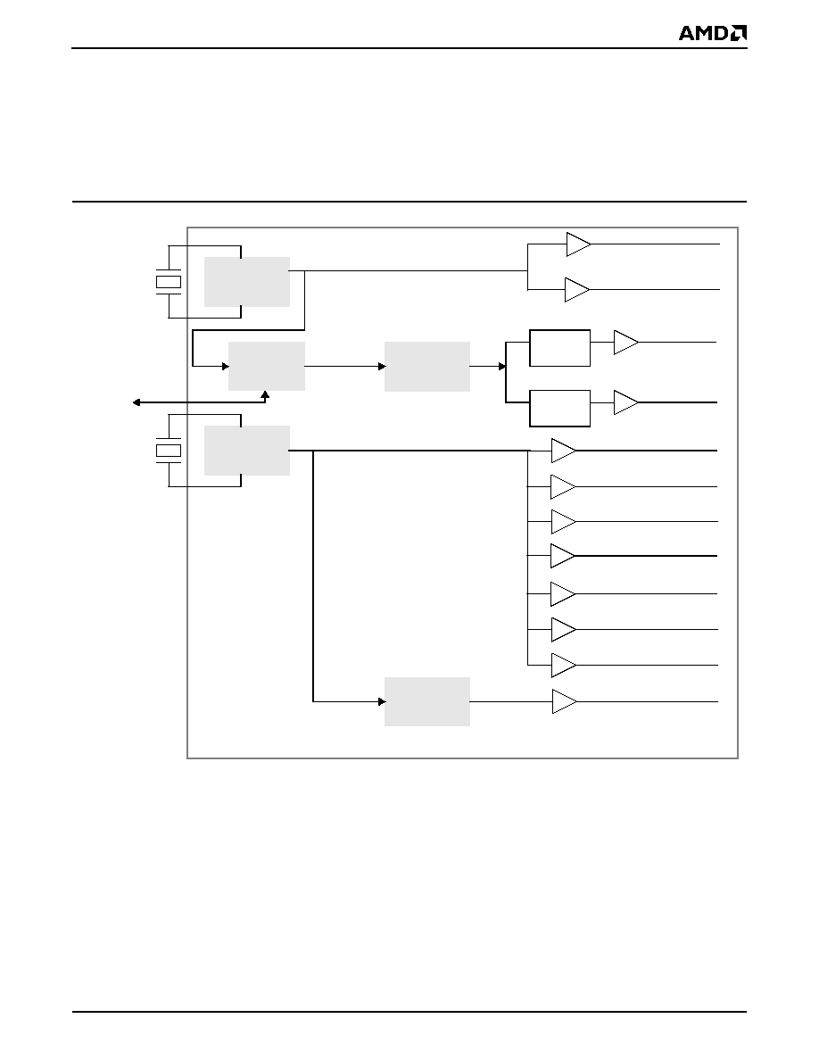
…lanTMSC520 Microcontroller Data Sheet
39
P R E L I M I N A R Y
Internal Clocks
Figure 7 shows a block diagram of the …lanSC520 mi-
crocontroller's internal clocks.
The clocks are generated from two local oscillators.
The 32.768-kHz oscillator is used to drive PLL1
(1.47456-MHz PLL), which in turn drives PLL2 (36.864-
MHz PLL). The 36.864-MHz clock is divided by 2 to
produce the 18.432-MHz UART clock. It is divided by
31 to produce the 1.1892-MHz PIT clock.
The 33-MHz oscillator produces the 33-MHz PCI and
CPU clocks. The 33-MHz oscillator is also used to drive
PLL3 (66-MHz PLL) to produce the SDRAM clock.
Figure 7.
Clock Source Block Diagram
32.768-kHz
Crystal
32.768-kHz
Oscillator
PLL2
1.47456 MHz
DIV 31
DIV 2
1.1892-MHz PIT
18.432-MHz UART
33-MHz
Oscillator
PLL3
32.768-kHz SDRAM Refresh
33-MHz
Crystal
36.864 MHz
LF_PLL1
32.768-kHz RTC
Notes:
1. Includes the programmable interval timer (PIT), general-purpose timers, watchdog timer, and the software timer.
PCI
CPU
SDRAM
GP Bus
GP DMA
ROM
SSI
33 MHz
33 MHz
33 MHz
33 MHz
33 MHz
33 MHz
66 MHz
PLL1
Timers
1
33 MHz
40
…lanTMSC520 Microcontroller Data Sheet
P R E L I M I N A R Y
Clock Specifications
PLL period jitter specifications are summarized in
Table 3. Jitter specifications are only guaranteed when
analog supply noise restrictions are met.
Table 4 shows PLL lock times and oscillator start-up
times.
Table 5 shows the oscillator input specifications.
Loop filter components for the 1.47456-MHz PLL (PLL1)
must be supplied externally. They are connected be-
tween the analog V
CC
(VCC_ANLG) and the …lanSC520
microcontroller pin, LF_PLL1. Specifications for
VCC_ANLG are shown in Table 6. Figure 6 on page 38
shows the loop filter circuit composed of C1, C2, and R1.
Component values are given in Table 7 on page 41.
Clock Pin Loading
The …lanSC520 microcontroller's clock driver pins are
designed to source or sink 24 mA. As shown in
Figure 6 on page 38, an external clock driver may be
necessary when the system presents a large capaci-
tive load.
Clock pads are designed to either source or sink 24
mA. The maximum amount of capacitive load that can
be placed on a clock pad is determined by the required
rise/fall times. Use the following equation to determine
the maximum capacitive loading.
C = I/(dV/dt)
where I = current, dV = voltage change, and dt = time
change.
As an example, suppose that the system requires a
rise/fall time of 1 ns, with a voltage swing of 2.5 V.
Then, the maximum capacitive load is:
C
MAX
= 24 mA/(2.5 V/1 ns) = 9.6 pF
Table 3.
Clock Jitter Specifications
Clock Name
Clock Frequency
Min
Nominal
Max
PIT
1.1892 MHz
828.3 ns
840.9 ns
853.5 ns
UART
18.432 MHz
53.44 ns
54.25 ns
55.07 ns
CPU
33.000 MHz or 33.333 MHz
--
250 ps
--
SDRAM
66.000 MHz or 66.666 MHz
14.775 ns
15.0 ns
15.225 ns
Table 4.
Clock Startup and Lock Times
Clock Source
Min
Typ
Max
32.768-kHz Oscillator
--
--
1 s
33-MHz Oscillator
--
--
10 ms
PLL1 (1.47456 MHz)
--
--
10 ms
PLL2 (36.864 MHz)
--
--
100
m
s
PLL3 (66 MHz)
--
--
50
m
s
Table 5.
Oscillator Input Specifications
Parameter
Min
Typ
Max
32KXTAL2 Input Voltage Low
≠0.3 V
--
+0.8 V
32KXTAL2 Input Voltage High
VCC_RTC ≠ 0.8 V
--
VCC_RTC + 0.3 V
33MXTAL2 Input Voltage Low
≠0.3 V
--
+0.8 V
33MXTAL2 Input Voltage High
VCC_ANLG ≠ 0.8 V
--
VCC_ANLG + 0.3 V
Table 6.
Analog VCC (VCC_ANLG) Specifications
Parameter
Min
Typ
Max
Peak-to-Peak Noise on VCC_ANLG
--
--
75 mV
VCC_ANLG Voltage Level
2.25 V
2.5 V
2.75 V
VCC_ANLG Current
1.4 mA
1.9 mA
2.1 mA

…lanTMSC520 Microcontroller Data Sheet
41
P R E L I M I N A R Y
Selecting a Crystal
The accuracy of the RTC depends on several factors
relating to crystal selection and board design. A clock
timing budget determines the clock accuracy. The de-
signer should determine the timing budget before se-
lecting a crystal.
There are four major contributors to a clock timing budget.
s
Frequency Tolerance--This is the crystal calibration
frequency. It states how far off the actual crystal
frequency is from the nominal frequency. For a typical
32.768-kHz crystal (watch crystal), the frequency
tolerance is ±20 parts per million (ppm). Frequency
tolerance is specified at room temperature.
s
Frequency Stability--This parameter is a
mea su re of h ow mu ch the cr ystal re so nan t
frequency is influenced by operating temperature.
For watch crystals, typical numbers are around ≠30
ppm over the temperature range.
s
Aging--This parameter is how much the crystal
resonant frequency changes with time. Typical
Aging numbers are ± 3 ppm per year.
s
Load Capacitance--The crystal is calibrated with a
specific load capacitance. If the system load
capacitance does not equal the cr ystal load
capacitance, a timing error is introduced. The timing
error is calculated by the following equation.
Error = {[1 + C1/(CL
xtal
+Co)]
1/2
≠ [1 +C1/
(CL
system
+Co)]
1/2
}/ [1 + C1/(CL
xtal
+Co)]
1/2
If you multiply Error by 10
6
, the error in ppm is given.
In the above equation, C1 is the crystal motional
capacitance, and Co is the crystal static
capacitance. CL
xtal
is the crystal load capacitance,
and CL
system
is the system load capacitance.
Once the complete timing error has been calculated
by adding all of the errors together, compare it to the
initial timing budget. Table 8 provides a convenient
translation of ppm to seconds per month.
32.768-kHz Crystal Selection
The 32.768-kHz crystal oscillator is shown in Figure 8.
The oscillator load capacitance is 5 pF. Table 9 pro-
vides specifications for selecting a proper 32.768-kHz
crystal. The Ecliptek ECPSM29T is recommended.
Figure 8.
32.768-kHz Crystal Circuit
Table 7.
PLL1 Loop Filter Components
Parameter
Min
Typ
Max
C1
0.009
m
F
0.01
m
F
0.011
m
F
C2
0.0009
m
F
0.001
m
F
0.0011
m
F
R1
4.465 k
W
4.7 k
W
4.935 k
W
Table 8.
Timing Error as It Translates to Clock
Accuracy
Timing Error
(Parts per million)
Seconds/Month
± 10
± 25.9
± 20
± 51.8
± 30
± 77.8
± 40
± 103.7
± 50
± 129.6
10 pF
10 pF
32.768-kHz Crystal
Internal
External
AMP
32KXTAL1
32KXTAL2
42
…lanTMSC520 Microcontroller Data Sheet
P R E L I M I N A R Y
33-MHz Crystal Selection
The same information related to the 32.768-kHz crystal
selection applies to the 33-MHz crystal selection. The
…lanSC520 microcontroller supports either a 33.000-
MHz or 33.333-MHz crystal. Specifications for the
33-MHz crystal are shown in Table 10.
AMD recommends using a fundamental mode 33.333-
MHz crystal. If a third overtone crystal is used, the os-
cillator gain may not be large enough to produce a reli-
able clock.
Third Overtone Crystal Component Selection
For the third overtone crystal circuit implementation,
refer to Figure 9 on page 43. Components C4 and L1
are selected by the user. C3 is a parasitic capacitor
composed of board parasitics. Typical values for C3
range from 5 pF to 15 pF.
C4 is required for DC isolation. A nominal value for C4
is 0.1
m
F.
L1 in conjunction with C3 and C2 form a resonant cir-
cuit. The value of L3 is selected so that the resonant
frequency is between the fundamental frequency and
the third overtone frequency. For a 33.333-MHz third
overtone crystal, the fundamental frequency is 11.111
MHz. From this, a desirable resonant frequency is be-
tween 11.111 MHz and 33.333 MHz. A good target fre-
quency is 22.222 MHz.
L1 is selected from the basic equation:
L1 = 1/[(2
º
Pi
º
frequency)
2
º
(C2 + C3)]
Assuming that the board parasitics are 15 pF, then:
L1 = 1/[ (2
º
Pi
º
22.222 MHz)
2
º
(7 pF + 15 pF)]
= 2.3
m
H
Table 9.
32.768-kHz Crystal Specifications
Parameter
Min
Typ
Max
Comment
Nominal Frequency
--
32.768 kHz
--
Effective Series Resistance (ESR)
--
--
60000
W
Drive Level
1
m
W
--
--
Load Capacitance
(…lanSC520 microcontroller)
4.5 pF
5 pF
5.5 pF
Resonant Mode
--
--
--
Parallel
Crystal Cut
--
--
--
BT
Operating Mode
--
--
--
Fundamental
Table 10.
33-MHz Crystal Specifications
Parameter or Characteristic
Min
Typ
Max
Comment
Nominal Frequency
33.000 MHz
--
33.333 MHz
ESR
--
--
40
W
Drive Level
1 mW
--
--
Load Capacitance
(…lanSC520 microcontroller)
--
2.5 pF
--
Resonant Mode
--
--
--
Parallel
Crystal Cut
--
--
--
AT or BT
Operating Mode
--
--
--
Fundamental

…lanTMSC520 Microcontroller Data Sheet
43
P R E L I M I N A R Y
Figure 9.
33.333-MHz Third Overtone Crystal Implementation
Running the …lanTMSC520 Microcontroller
at 33.333 MHz
The clock that is supplied to the PCI bus (CLKPCIOUT)
is exactly the same as the frequency of the crystal. The
…lanSC520 microcontroller simply buffers the 33-MHz
crystal input and provides it to the CLKPCIOUT pin.
Since crystals have inaccuracies, it is possible that
these inaccuracies cause the period of CLKPCIOUT to
become marginally less than 30 ns.
It is up to the system designer to choose the accuracy
of the crystal used with the …lanSC520 microcontroller.
The 33.000-MHz frequency provides a better guard
band than the 33.333-MHz crystal. In practice, most
PCI devices can tolerate both frequencies, but it is im-
portant to be aware of the impact of choosing the crys-
t a l o n t h is p o t e n t i a l v i o l a t i o n o f t h e P C I bu s
specifications. The PCI bus specification requires that
the minimum clock period be 30 ns.
Internal
External
AMP
33MXTAL1
33MXTAL2
C4 = 0.1
m
F
L1
C3
C1 =7 pF
C2 = 7 pF
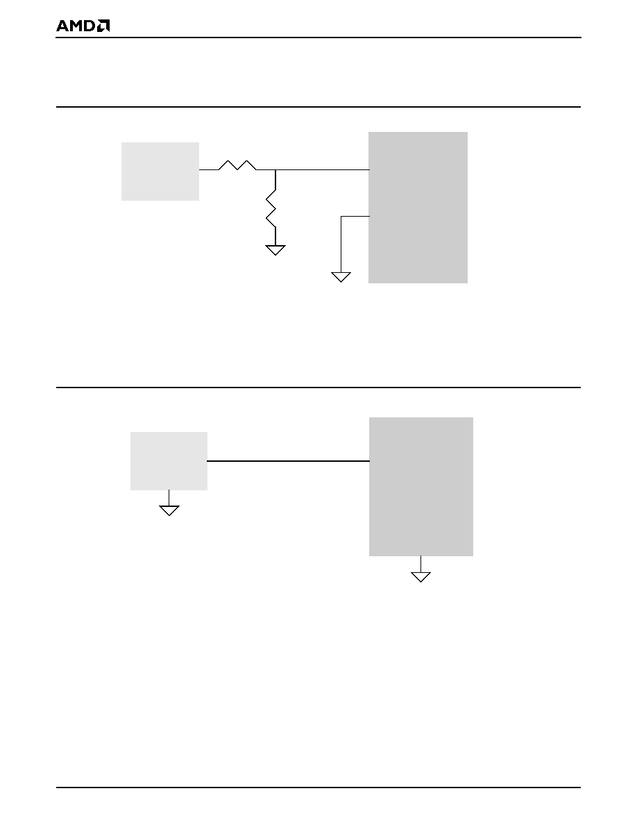
44
…lanTMSC520 Microcontroller Data Sheet
P R E L I M I N A R Y
Bypassing Internal Oscillators
The 32.768-kHz and the 33-MHz …lanSC520 micro-
controller oscillators can be bypassed by connecting an
external clock to the crystal pins. Refer to Figure 10
and Figure 11 for the suggested circuitry.
Figure 10.
Bypassing the 32.768-kHz Oscillator
Figure 11.
Bypassing the 33-MHz Oscillator
32KXTAL2
32KXTAL1
100 k
…lanSC520
Microcontroller
2.5 V ±10% typical
External
32.768-kHz
Oscillator
R2
R1
Note: R1 and R2 are required when the external oscillator voltage, V
OSC
, exceeds 2.5 V. The
value of R1 depends on V
OSC
according to the formula R1 = 100 k
(V
OSC
≠ 2.5) / 2.5, where 100
k
is the fixed value of R2, and 2.5 is the typical voltage for 32KXTAL2 (
±10%)
.
No Connect
33MXTAL2
33MXTAL1
…lanSC520
Microcontroller
2.5-V ±10% typical
External
33-MHz
Oscillator

…lanTMSC520 Microcontroller Data Sheet
45
P R E L I M I N A R Y
Figure 12.
RTC Voltage Monitor Block Diagram
RTC VOLTAGE MONITOR
If an external backup battery is connected to the
…lanSC520 microcontroller's VCC_RTC pin, the real-
time clock (RTC) remains operational even if all the
other power supplies are turned off. The …lanSC520
microcontroller's RTC voltage monitor is designed to
signal the RTC core when the backup battery is not in-
stalled or is low. Additionally, the voltage monitor circuit
signals the RTC core when the rest of the system is
being powered down.
Features of the voltage monitor include:
s
Bandgap voltage generator for precision reference
voltage
s
High-gain amplifier for adjusting bandgap voltage to
"low battery" trip voltage
s
The RTC can be connected to the main power plane
if a backup battery is not needed in the system.
Figure 12 shows a block diagram of the RTC voltage
monitor.
The voltage monitor circuit uses a delta Vbe voltage
(voltage from base to emitter) source to generate a
bandgap voltage of approximately 1.23 V. This voltage
is the input to an amplifier whose gain is such that the
output voltage is a 2-V reference. This reference signal
is an input to a comparator, along with the backup bat-
tery voltage, BBATSEN. If BBATSEN drops below the
2-V reference, an RTC invalidate signal is generated to
notify the user via the RTC_VRT bit (RTC index 0Dh[7])
that the RTC contents are no longer valid.
There are three conditions that trigger an RTC invalida-
tion. They are the following:
s
BBATSEN drops below 2 V (sampled when PWR-
GOOD asserts)--During operation from the main
power supply, the backup battery voltage might
drop below the trip voltage (2 V). The RTC is not in-
validated until a PWRGOOD assertion occurs.
s
Power is applied to VCC_RTC (the backup battery
is plugged in)--When the backup battery is plugged
in, the RTC is immediately invalidated.
s
No battery during power-up (sampled after PWR-
GOOD asserts)--If the system does not contain a
backup battery and the BBATSEN line potential is
below 2 V, the RTC is invalidated when PWRGOOD
asserts.
In addition to the backup battery monitor function, the
voltage monitor also provides a power-down signal to
the RTC. This signal is used to isolate the RTC core from
the rest of the integrated peripherals. A timing diagram
for this sequence is shown in Figure 27 on page 60.
+
≠
Bandgap
VBG
Amplifier
BBATSEN
One-
Shot
RTC Reset
Flip-
Flop
D
CK
Q
PWRGOOD
32 kHz
Internal RTC Power-Down
2.0 V
Voltage
Generator
46
…lanTMSC520 Microcontroller Data Sheet
P R E L I M I N A R Y
Backup Battery Considerations
The behavior of the RTC when the primary power sup-
ply is turned off depends on whether or not an external
backup battery is included in the system design.
Using an External RTC Backup Battery
An implementation using a backup battery is shown in
Figure 13 on page 47. The primary power source for
VCC_RTC is the main power plane (VCC). D1 should be
chosen so that the forward voltage drop is small, less
than 0.25 V. D1 also prevents the backup battery from
powering up the VCC power plane when the main sup-
ply is turned off.
The backup battery voltage must not exceed 3.3 V (af-
fects the BBATSEN and VCC_RTC pins); higher volt-
ages may damage the …lanSC520 microcontroller.
The RC network composed of R1 and C2 provides a
time delay for the internal circuit power-up sequence.
Accuracy tolerances are
±
10% of nominal values given
in Table 11. C1 is for high-frequency filtering purposes.
Not Using an External RTC Backup Battery
For the system that is not using a backup battery,
Figure 14 on page 47 shows how the circuit should be
designed. It uses the same RC that is needed by the
battery system, but it is now connected to VCC_RTC.
For this configuration, the RTC is invalidated after
power-up, but is not invalidated by subsequent PWR-
GOOD assertions.
s
The RTC is invalidated after a power-up. In this
case, power has been removed from the RTC, so it
should be invalidated.
s
When a reset switch tied to PWRGOOD is pressed
(V
CC
remains High), PWRGOOD reasserts with
BBATSEN High, so the RTC is not invalidated. In
this case, power did not go away, so the RTC con-
tents are still good.
VCC_ANLG is selected as the power plane for
VCC_RTC because it is a well-filtered power plane that
is well below the VCC_RTC maximum of 3.3 V.
Component values for the resistor and capacitor are
shown in Table 11.
Table 11.
RTC Voltage Monitor Component Specifications
Component
Parameter
Min
Nominal
Max
D1
Forward Voltage Drop
--
0.25 V
--
D2
Forward Voltage Drop
--
Note
1
--
D1, D2
Forward Current
--
100
m
A
--
C1
Capacitance
5 pF
10 pF
20 pF
C2
Capacitance
180 pF
200 pF
400 pF
R1
Resistance
900
1 k
W
1.1 k
W
Notes:
1. Diode should be selected so that the voltage into the RTC power pin (VCC_RTC) does not exceed 3.3 V.
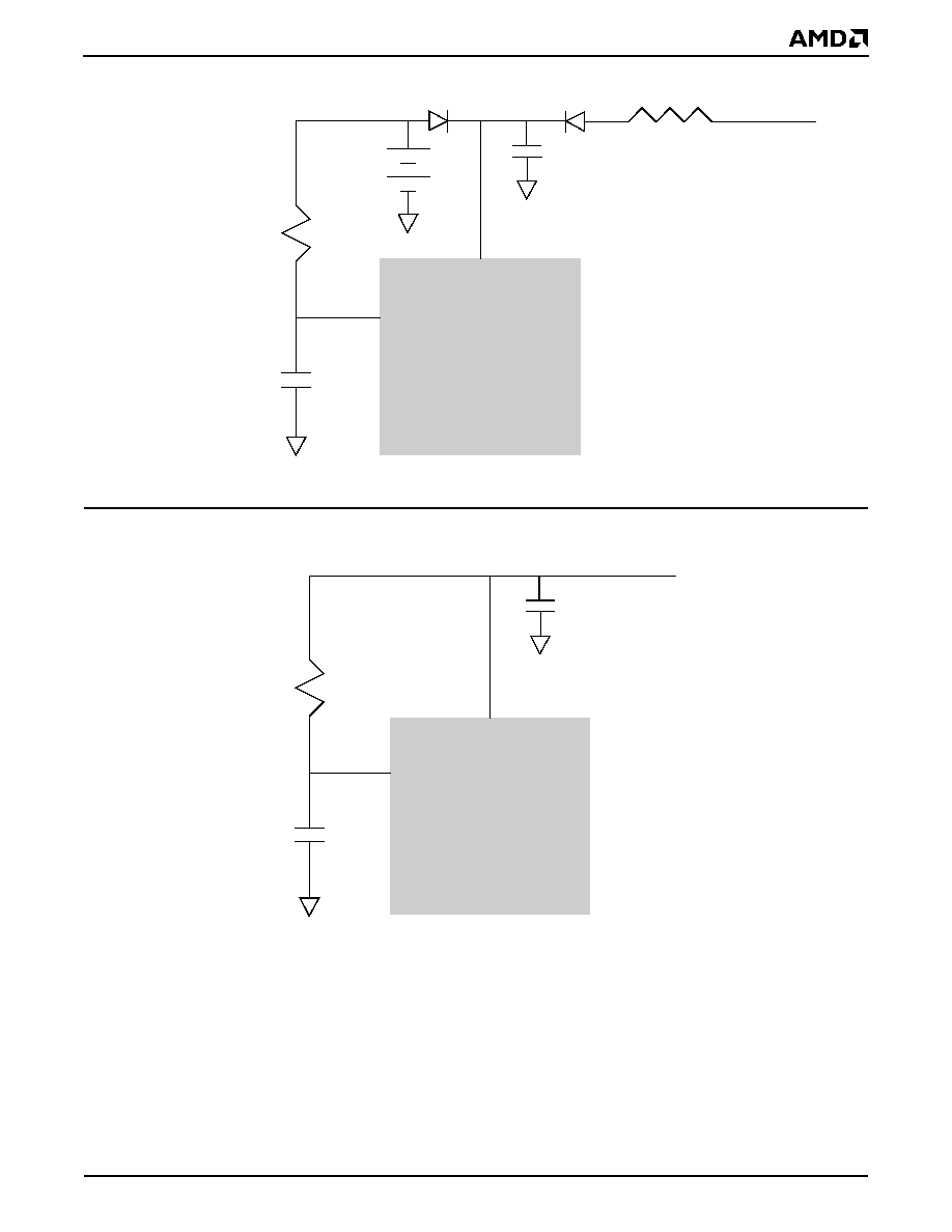
…lanTMSC520 Microcontroller Data Sheet
47
P R E L I M I N A R Y
Figure 13.
Circuit with Backup Battery
Figure 14.
Circuit without Backup Battery
BATT
VCC_RTC
VCC_RTC
BBATSEN
C1
D1
D2
R1
C2
(3.3 V max)
10
…lanSC520 Microcontroller
VCC_ANLG
C1
R1
C2
…lanSC520 Microcontroller
VCC_RTC
BBATSEN
48
…lanTMSC520 Microcontroller Data Sheet
P R E L I M I N A R Y
ABSOLUTE MAXIMUM RATINGS
1
Notes:
1. WARNING--the "Absolute Maximum Ratings" are stress ratings only. Stresses above those listed can cause permanent dam-
age. Operation beyond the values specified in Operating Ranges at Commercial Temperatures is not recommended, and ex-
tended exposure beyond these operating range values can affect device reliability.
Symbol
Parameter
Minimum
Maximum
Unit
--
Storage temperature
≠65
+125
∞C
VCC_CORE
Core voltage
2
2. Referenced from GND.
≠0.5
3.2
V
VCC_I/O
I/O voltage
2,3
3. All inputs are 5-V tolerant.
≠0.5
5.5
V
VCC_RTC
Real-time clock voltage
2
≠0.5
4.5
V
VCC_ANLG
Analog voltage
2
≠0.5
3.2
V
OPERATING RANGES AT COMMERCIAL TEMPERATURES
1
Notes:
1. Operating ranges define the temperature and voltage limits between which the functionality of the device is guaranteed.
Symbol
Parameter Description
Minimum
Typical
Maximum
Unit
T
CASE
Commercial case temperature operating in free air
0
--
+85
∞C
VCC_CORE
Core voltage
2
2. Referenced from GND.
+2.375
+2.5
+2.625
V
VCC_I/O
I/O voltage
2,3
3. All inputs are 5-V tolerant.
+3.0
+3.3
+3.6
V
VCC_RTC
Real-time clock voltage
2
+2.0
+2.5
+3.3
V
VCC_ANLG
Analog voltage
2
+2.25
+2.5
+2.75
V

…lanTMSC520 Microcontroller Data Sheet
49
P R E L I M I N A R Y
VOLTAGE LEVELS FOR PCI INTERFACE PINS
The voltage characteristics of the PCI interface input
pins are specified in the PCI Local Bus Specification,
Revision 2.2, section 4.2.1 5V Signaling Environment
and section 4.2.2 3.3V Signaling Environment.
The voltage characteristics of the PCI interface output
pins are specified in the PCI Local Bus Specification,
Revision 2.2, 4.2.2 3.3V Signaling Environment.
VOLTAGE LEVELS FOR NON-PCI INTERFACE PINS
1
Notes:
1. The drive strengths of all the pins are listed in Table 20, "Pin List Summary," on page A-7. The pins with variable drive strengths
can take on the characteristics of 12-, 18-, or 24-mA signals.
Advance Information
Unit
Symbol
Parameter Description
Min
Max
V
IL
Input Low voltage
≠ 0.3
+ 0.8
V
V
IH
Input High voltage
2.0
VCC_I/O
+ 1.7
V
V
OH1
Output High voltage (I
OH
= ≠6 mA)
VCC_I/O ≠ 0.45
--
V
V
OL1
Output Low voltage (I
OL
= 6 mA)
--
0.45
V
V
OH2
Output High voltage (I
OH
= ≠12 mA)
VCC_I/O ≠ 0.45
--
V
V
OL2
Output Low voltage (I
OL
= 12 mA)
--
0.45
V
V
OH3
Output High voltage (I
OH
= ≠18 mA)
VCC_I/O
≠ 0.45
--
V
V
OL3
Output Low voltage (I
OL
= 18 mA)
--
0.45
V
V
OH4
Output High voltage (I
OH
= ≠24 mA)
VCC_I/O ≠ 0.45
--
V
V
OL4
Output Low voltage (I
OL
= 24 mA)
--
0.45
V

50
…lanTMSC520 Microcontroller Data Sheet
P R E L I M I N A R Y
DC CHARACTERISTICS OVER COMMERCIAL OPERATING RANGES
Notes
Advance Information
Unit
Symbol
Parameter Description
Min
Typ
Max
I
CC
_CORE
Current for VCC_CORE supply @ 133 MHz
--
465
660
mA
I
CC
_CORE
Current for VCC_CORE supply @ 100 MHz
--
380
540
mA
I
CC
_I/O
Current for VCC_ I/O supply @ 33-MHz
1
Notes:
1. Estimate based on 3.3-V operation. Current for the I/O supply is constant, independent of the CPU frequency.
--
100
120
mA
I
CC
_RTC
Current for RTC-only mode
2 , 3
2. Value determined by simulation will be updated once characterization is complete.
3. Current measured with power applied only to the VCC_RTC supplies.
--
5
--
m
A
I
CC
_ANLG
Current for ANLG-only mode
1.4
1.9
2.1
mA
I
LI1
Input leakage current (0.1 V < V
IN
< VCC_I/O)
(All pins except those with internal pullup or
pulldown resistors)
4 , 5
4. VCC_I/O = 3.6 V.
5. Table 20, "Pin List Summary," on page A-7 shows which pins have internal pullups or pulldowns.
--
--
È
20
m
A
I
LI2
Input leakage current V
IN
= (VCC_I/O ≠ 0.1 V)
(All pins with internal pulldown resistors)
4, 5
--
--
60
m
A
I
LI3
Input leakage current V
IN
= 0.1 V
(All pins with internal pullup resistors)
5
--
--
≠60
m
A
I
LO
Output leakage current
--
--
±15
m
A
…lanTMSC520 Microcontroller Data Sheet
51
P R E L I M I N A R Y
CAPACITANCE
PCI Interface Pin Capacitance
Pin capacitance values are specified in the
PCI Local
Bus Specification
, Revision 2.2, section 4.2.2.1 DC
Specifications, Table 4-3: DC Specifications for 3.3V
Signaling.
Crystal Capacitance
The crystal specifications can be found in Table 9,
"32.768-kHz Crystal Specifications" on page 42 and
Table 10, "33-MHz Crystal Specifications" on page 42.
Derating Curves
All programmable I/O pins can be driven to the maxi-
mum drive current at once.
The derating curves on the following pages can be
used to determine potential specified timing variations
based on system capacitive loading. Table 20, "Pin List
Summary," on page A-7 has a column named "Max
Load (pF)." This column describes the specification
load presented to the specific pin, when testing was
performed, to generate the timing specification docu-
mented in the AC Characteristics section of this data
sheet.
If the capacitive load on GPA0 is 70 pF, then a typical
rise time is 6.5 ns. From Figure 18, the same load gives
a typical fall time of 7 ns.
Non-PCI Interface Pin Capacitance
Advance Information
Unit
Symbol
Parameter Description
Test Conditions
Min
Max
C
IN
Input capacitance
F
C
=1 MHz
--
10
pF
C
32KXTAL
32KXTAL1, 33KXTAL2 pin capacitance
--
20
pF
C
33MXTAL
33MXTAL1, 33MXTAL2 pin capacitance
--
15
pF
C
OUT
Output capacitance
--
10
pF
C
IO
I/O pin capacitance
--
10
pF

52
…lanTMSC520 Microcontroller Data Sheet
P R E L I M I N A R Y
Figure 15.
I/O Drive 6-mA Rise Time
Figure 16.
I/O Drive 6-mA Fall Time
0
5
10
15
20
25
30
35
0
20
40
60
80
100
120
pF
ns
Worst Case
Typical
0
5
10
15
20
25
30
35
pF
ns
Worst Case
Typical

…lanTMSC520 Microcontroller Data Sheet
53
P R E L I M I N A R Y
Figure 17.
I/O Drive 12-mA Rise Time
Figure 18.
I/O Drive 12-mA Fall Time
0
2
4
6
8
10
12
14
16
18
0
20
40
60
80
100
120
pF
ns
Worst Case
Typical
0
2
4
6
8
10
12
14
16
18
0
20
40
60
80
100
120
pF
ns
Worst Case
Typical
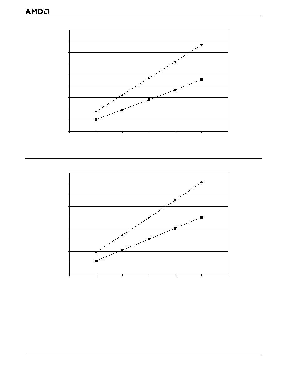
54
…lanTMSC520 Microcontroller Data Sheet
P R E L I M I N A R Y
Figure 19.
I/O Drive 24-mA Rise Time
Figure 20.
I/O Drive 24-mA Fall Time
0
1
2
3
4
5
6
7
8
9
0
20
40
60
80
100
120
pF
ns
Worst Case
Typical
0
1
2
3
4
5
6
7
8
9
0
20
40
60
80
100
120
pF
ns
Worst Case
Typical

…lanTMSC520 Microcontroller Data Sheet
55
P R E L I M I N A R Y
Figure 21.
PCI Pads Rise Time with 1-ns Rise/Fall
Figure 22.
PCI Pads Fall Time with 1-ns Rise/Fall
0
1
2
3
4
5
6
7
0
10
20
30
40
50
60
pF
ns
Worst Case
Typical
Best Case
0
0.5
1
1.5
2
2.5
3
3.5
4
0
10
20
30
40
50
60
pF
ns
Best Case
Worst Case
Typical

56
…lanTMSC520 Microcontroller Data Sheet
P R E L I M I N A R Y
POWER CHARACTERISTICS
Dynamic I
CC
measurements are dependent upon chip
activity, operating frequency, output buffer logic, and
capacitive/resistive loading of the outputs. Actual
power supply current is dependent on system design
and may be greater or less than the typical I
CC
number
present here. Maximum power is measured at maxi-
mum V
CC
at maximum case temperature. Typical
power is measured at typical V
CC
at 55∞C. For power
dissipation values, refer to Table 12 and Table 13.
THERMAL CHARACTERISTICS
388-Pin PBGA Package
The …lanSC520 microcontroller is specified for opera-
tion with case temperature ranges from 0
C to +85
C
for VCC_CORE = 2.5 V ± 10% and VCC_I/O = 3.3 V ±
10%. Case temperature is measured at the top center
of the package as shown in Figure 23. The various
temperatures and thermal resistances can be deter-
mined using the equations in Figure 24 with informa-
tion given in Table 15.
Thermal, electrical, and mechanical characteristics of
AMD qualified packages (including the 388 PBGA) can
be found on AMD's website at www.amd.com. Click on
the link Products, and then click on the document link
Packages and Packing Methodologies.
Figure 23.
Thermal Resistance (
C/Watt)
Table 12.
Device Power Dissipation
1
Notes:
1. Device power dissipation calculation assumes that 50% of the I/O power is
consumed on chip.
Power
100 MHz
133 MHz
Unit
Maximum power
1.7
2.0
W
Typical power
1.2
1.4
W
Table 13.
VCC_ANLG and VCC_RTC Power Dissipation
Supply
Typical
Max
Unit
VCC_ANLG voltage level
2.5
2.75
V
VCC_ANLG current
1.9
2.1
mA
VCC_ANLG power
4.75
5.78
mW
VCC_RTC voltage level
2.5
3.3
V
VCC_RTC current
5
--
m
A
VCC_RTC power
12.5
--
m
W
q
JA
q
CA
q
JC
q
JA
=
q
JC
+
q
CA
T
C

…lanTMSC520 Microcontroller Data Sheet
57
P R E L I M I N A R Y
Table 14.
Thermal Resistance (∞C/W)
q
JC
and
q
JA
for BGA Package with 6-Layer Board
Board Type
1
Notes:
1. The board type is described in the JEDEC standards document entitled Thermal Test
Chip Guideline (Wire Bond Type Chip) at www.jedec.org. On the home page click on
the link Free Standards and Docs, and then click on the document link JESD51-4
under JEDEC PUBLICATIONS.
q
JC
q
JA
vs. Airflow
0
200
400
600
800
6-layer
3.3
16.6
14.7
13.6
12.9
12.5
Table 15.
Maximum T
A
for Plastic BGA Package
with 6-Layer Board
1
with T
CASE
= 85∞C
Notes:
1. The board type is described in the JEDEC standards document entitled Thermal Test
Chip Guideline (Wire Bond Type Chip)
at www.jedec.org. On the home page click on
the link Free Standards and Docs, and then click on the document link JESD51-4 under
JEDEC PUBLICATIONS.
CPU Clock Rate
Airflow (Linear Feet Per Minute)
0
200
400
600
800
133 MHz
67∞C
70∞C
71∞C
72∞C
73∞C
100 MHz
70∞C
72∞C
74∞C
74∞C
75∞C
q
JA
=
q
JC
+
q
CA
P = I
CC
º
V
CC
T
J
= T
C
+ (P
º
q
JC
)
T
J
= T
A
+ (P
º
q
JA
)
where:
q
JA
= Thermal resistance from junction to ambient
q
JC
= Thermal resistance from junction to case
q
CA
= Thermal resistance from case to ambient
T
J
= Junction temperature
T
A
= Ambient temperature
T
C
= Case temperature
P = Power in Watts
I
CC
= Power supply current in mA
Figure 24.
Thermal Characteristics Equations
58
…lanTMSC520 Microcontroller Data Sheet
P R E L I M I N A R Y
SWITCHING CHARACTERISTICS AND WAVEFORMS
The AC switching specifications provided in the AC
characteristics tables that follow consist of output de-
lays, input setup requirements, and input hold require-
ments.
AC specifications measurement is defined by the fig-
ures that follow each timing table. All timings are refer-
enced to 1.5 V unless otherwise specified.
Output delays are specified with minimum and maxi-
mum limits, measured as shown. The minimum delay
times are hold times provided to external circuitry.
Input setup and hold times are specified as minimums,
defining the smallest acceptable sampling window.
Within the sampling window, a synchronous input sig-
nal must be stable for correct microcontroller operation.
AC SWITCHING TEST WAVEFORMS
Non-PCI Bus Interface Pins
Figure 25.
AC Switching Test Waveforms
PCI Bus Interface Pins
For AC timing for PCI bus interface pins, refer to the
PCI Local Bus Specification
, Revision 2.2, 4.2.3.3
Measurement and Test Conditions, Figure 4-7: Output
Timing Measurement Conditions, and Figure 4-8: Input
Timing Measurement Conditions.
Key to Switching Waveforms
WAVEFORMS
INPUTS
OUTPUTS
Must be Steady
Will be Steady
May Change from H to L
Will be Changing from H to L
May Change from L to H
Will be Changing from L to H
Don't Care, Any Change Permitted
Changing, State Unknown
Does Not Apply
Center Line is High-Impedance "Off" State
VCC_I/O
2
VCC_I/O
2
V
IH
= VCC_I/O
Input
V
IL
= 0
Test Points
Output
Note: For AC testing, inputs are driven at 3 V for a logic 1 and 0 V for a logic 0.
…lanTMSC520 Microcontroller Data Sheet
59
P R E L I M I N A R Y
SWITCHING CHARACTERISTICS OVER COMMERCIAL OPERATING RANGES
In this section, the following timings and timing wave-
forms are shown:
s
Power-on reset (page 59)
s
Reset (page 61)
s
ROM (page 63)
s
PCI bus (page 65)
s
SDRAM (page 66)
s
SDRAM clock (page 68)
s
GP bus (page 69)
s
GP bus DMA read (page 71)
s
GP bus DMA write (page 72)
s
SSI (page 73)
s
JTAG (page 74)
Power-On Reset Timing
Symbol
Parameter Description
Notes
Advance Information
Unit
Min
Typ
Max
t1
VCC_RTC valid hold before all other V
CC
s are
valid
0
--
--
--
t2
PWRGOOD valid hold from all V
CC
valid
(except VCC_RTC)
1
--
1
--
s
t3
VCC_RTC valid to BBATSEN active
2
100
--
--
m
s
t4
CFGx, RSTLDx, DEBUG_ENTER,
INST_TRCE, AMDEBUG_DIS setup to
PWRGOOD active
5
--
--
ns
t5
CFGx, RSTLDx, DEBUG_ENTER,
INST_TRCE, AMDEBUG_DIS hold from
PWRGOOD active
5
--
--
ns
t6
GPRESET inactive from PWRGOOD active
10
--
11
ms
t7
RST inactive from PWRGOOD active
10
--
11
ms
t8
PWRGOOD inactive to all V
CC
s invalid
(except VCC_RTC)
3
33
--
--
m
s
Notes:
1. This parameter is dependent on the 32-kHz oscillator startup time, which is dependent on the characteristics of the crystal,
leakage and capacitive coupling on the board, and ambient temperature.
2. This parameter ensures that the internal RTC valid status bit is cleared to indicate that the RTC time and CMOS contents are
invalid.
3. This parameter must be met to ensure that the RTC date and time are not invalidated.

60
…lanTMSC520 Microcontroller Data Sheet
P R E L I M I N A R Y
Figure 26.
Power-Up Timing Sequence
Figure 27.
PWRGOOD Timing for RTC Standalone Mode
t4
t5
t1
t2
t3
t6
t7
VCC_RTC
All other V
CC
s
PWRGOOD
CFGx, RSTLDx,
BBATSEN
GPRESET
RST
DEBUG_ENTER,
INST_TRCE,
AMDEBUG_DIS
PWRGOOD
VCC
1
32 kHz
2.5 V
2.0 V
t8
Notes:
2. Applies to all V
CC
s except for VCC_RTC, which is left on for this mode.
3. These timings apply only when powering down the chip while leaving only the RTC powered.
4. Guarantees at least one rising edge on the 32-kHz signal after reset before 2 V is reached.
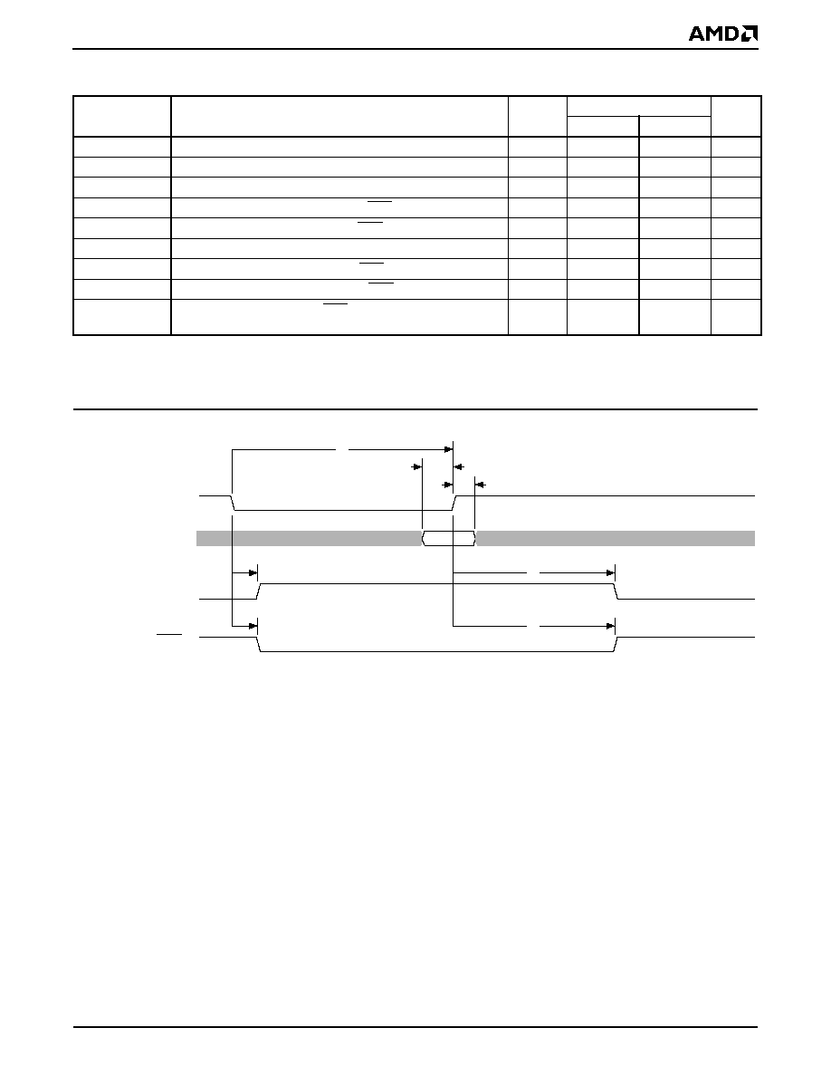
…lanTMSC520 Microcontroller Data Sheet
61
P R E L I M I N A R Y
Figure 28.
External System Reset Timing with Power Applied
Reset Timing with Power Applied
Symbol
Parameter Description
Notes
Advance Information
Unit
Min
Max
t1
PWRGOOD inactive pulse width
20
--
ns
t2
CFGx, RSTLDx setup to PWRGOOD active
5
--
ns
t3
CFGx, RSTLDx hold from PWRGOOD active
5
--
ns
t4
PWRGOOD inactive to GPRESET, RST outputs active
--
20
ns
t5
PWRGOOD active to GPRESET, RST outputs inactive
10
--
ms
t6
PRGRESET active pulse width
40
--
ns
t7
PRGRESET active to GPRESET, RST outputs active
90
1000
ns
t8
PRGRESET inactive to GPRESET, RST outputs inactive
10
--
ms
t9
Reset outputs (GPRESET, RST) active pulse width for
internally generated system reset
1
Notes:
1. Internal system reset sources include software system reset (SYS_RST bit), AMDebug interface system reset, and watchdog
timer reset.
10
11
ms
t2
t3
t1
t4
t5
t4
t5
PWRGOOD
CFGx, RSTLDx
GPRESET
RST
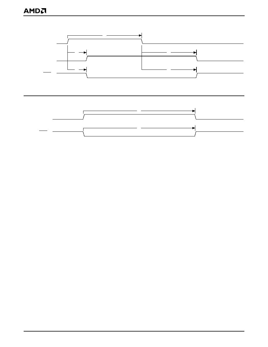
62
…lanTMSC520 Microcontroller Data Sheet
P R E L I M I N A R Y
Figure 29.
PRGRESET Timing
Figure 30.
Internal System Reset Timing
t6
t7
t8
t7
t8
PRGRESET
GPRESET
RST
t9
t9
GPRESET
RST
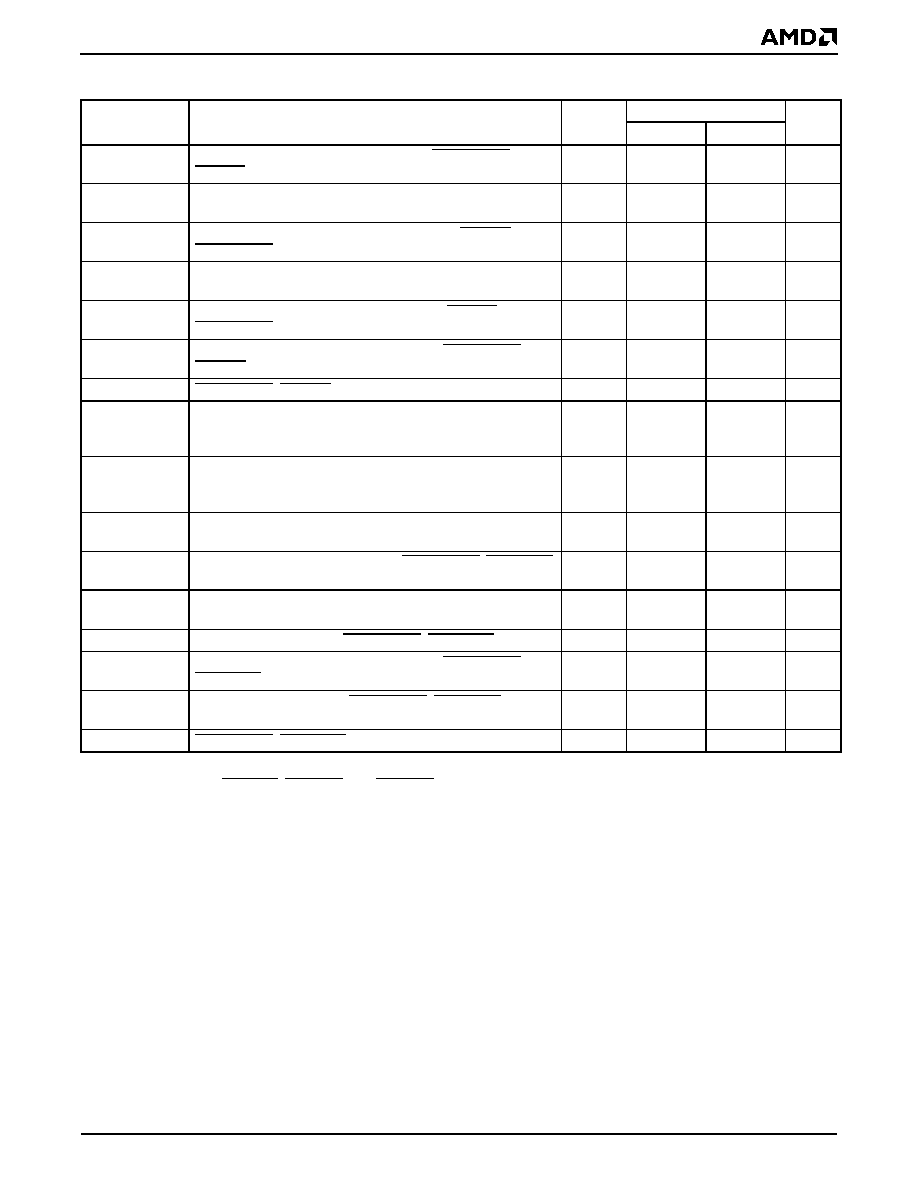
…lanTMSC520 Microcontroller Data Sheet
63
P R E L I M I N A R Y
ROM Timing
Symbol
Parameter Description
1
Notes
Advance Information
Unit
Min
Max
t1
GPA25≠GPA4, chip select setup before ROMBUFOE,
ROMRD, GPA3≠GPA0 active
10
--
ns
t2
GPA25≠GPA4, chip select active pulse-width read access
2
(P
FWS
+ 1)
∑ 30
3
--
ns
t3
Read data valid required from GPA3≠GPA0, ROMRD and
ROMBUFOE, non-page-mode access
2
--
((P
FWS
+ 1)
∑ 30
3
) ≠ 20
ns
t4
Read data valid from GPA3≠GPA0, page-mode access
4
--
((P
SWS
+ 1)
∑ 30
3
) ≠ 20
ns
t5
Read data hold from address, chip select, ROMRD, and
ROMBUFOE
0
--
ns
t6
GPA25≠GPA0, chip select hold time from ROMBUFOE,
ROMRD read access
0
--
ns
t7
ROMBUFOE, ROMRD read recovery time
25
--
ns
t8
GPA3≠GPA0 valid, first access
2
((P
FWS
+
1) ∑ 30
3
) ≠
5
--
ns
t9
GPA3≠GPA0 valid time, non-page-mode access
2
((P
FWS
+
1) ∑ 30
3
) ≠
5
--
ns
t10
GPA3≠GPA0 valid time, page-mode access
4
((P
SWS
+ 1)
∑ 30
3
) ≠ 5
--
ns
t11
GPA25≠GPA0, chip select setup to ROMBUFOE, FLASHWR
active
25
--
ns
t12
GPA25≠GPA0 valid, chip select active pulse-width write
access
2
(P
FWS
+ 2)
∑ 30
3
--
ns
t13
Write data valid setup to ROMBUFOE, FLASHWR
15
--
ns
t14
GPA25≠GPA0, chip select hold time from ROMBUFOE,
FLASHWR write access
15
--
ns
t15
Write data hold time from ROMBUFOE, FLASHWR write
access
15
--
ns
t16
ROMBUFOE, FLASHWR write recovery time
45
--
ns
Notes:
1. Chip Select includes BOOTCS, ROMCS1, and ROMCS2.
2. P
FWS
represents the programmable first wait state timing parameter in the ROM controller register for the corresponding ROM
chip select.
3. The value of 30 corresponds to the 33-MHz crystal frequency and assumes 33.333 MHz.
4. P
SWS
represents the programmable subsequent wait state timing parameter in the ROM controller register for the correspond-
ing ROM chip select.
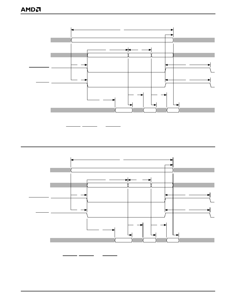
64
…lanTMSC520 Microcontroller Data Sheet
P R E L I M I N A R Y
Figure 31.
Non-Burst ROM Read Cycle Timing
Figure 32.
Page-Mode ROM Read Cycle Timing
t2
t9
t7
t7
t6
t8
t1
t1
t3
t5
t3
t5
t3
t5
GPA3≠GPA0
ROMBUFOE
ROMRD
GPA25≠GPA4,
Chip Select
Notes:
1. Chip select includes BOOTCS, ROMCS1, and ROMCS2.
2. Data includes GPD15≠GPD0 or MD31≠MD0.
DATA
(In)
t2
t10
t7
t7
t6
t8
t1
t1
t3
t5
t4
t5
t4
t5
GPA3≠GPA0
ROMBUFOE
ROMRD
Notes:
1. Chip select includes BOOTCS, ROMCS1, and ROMCS2.
2. Data includes GPD15≠GPD0 or MD31≠MD0.
DATA
(In)
GPA25≠GPA4,
Chip Select

…lanTMSC520 Microcontroller Data Sheet
65
P R E L I M I N A R Y
Figure 33.
Flash Write Cycle Timing
PCI Bus Timing
The characteristics of the PCI interface pins are speci-
fied in the
PCI Local Bus Specification
, Revision 2.2,
section 4.2.1.1 DC Specifications, Table 4-1: DC Spec-
ifications for 5V Signaling, and section 4.2.2.1 DC
Specifications, Table 4-3: DC Specifications for 3.3V
Signaling.
t12
t16
t13
t16
t14
t11
t11
t15
ROMBUFOE
FLASHWR
GPA25≠GPA0,
Chip Select
DATA
(Out)
Notes:
1. Chip select includes BOOTCS, ROMCS1, and ROMCS2.
2. Data includes GPD15≠GPD0 or MD31≠MD0.
66
…lanTMSC520 Microcontroller Data Sheet
P R E L I M I N A R Y
SDRAM Timing
Symbol
Parameter
Name
Parameter Description
Notes
Advance
Information
Unit
Min
Max
t1
T
RC
Refresh active to active command period T
RC
135
1
Notes:
1. Corresponds to the 33-MHz crystal frequency and assumes 33.333 MHz with no guardband.
--
ns
t2
T
RAS
Active command to precharge command period T
RAS
75
1
7500
ns
t3
T
RCD
Active command to column command same bank T
RCD
30
1
--
ns
t4
T
RP
Precharge command to active command period T
RP
30
1
--
ns
t5
T
DPL
Write recovery or data-in to precharge lead time T
DPL
30
1
--
ns
t6
T
CKH
CK High pulse width T
CKH
7
--
ns
t7
T
CKL
CK Low pulse width T
CKL
7
--
ns
t8
T
CK
CK period T
CK
15
1
--
ns
t9
T
CS
Command setup T
CS
5
--
ns
t10
T
CH
Command hold T
CH
2
--
ns
t11
T
AC
Access time from CK T
AC
2
2. This access time is based on the clock period assuming minimal delay between the CLKMEMOUT output and the CLKMEMIN
input. It does not take into account external delays for clock buffering/skew, clock loading/routing, and data loading/routing.
The delays that the system designer must take into consideration are identified by the equation below:
T
AC +
T
SKEW +
T
CK_LD +
T
D_LD <=
T
CK
where:
T
AC
= Access time of SDRAM device (not impacted by board design)
T
SKEW
= Delay between CLKMEMOUT to CLKMEMIN
T
CK_LD
= Additional clock delay due to loading
T
D_LD
= Data delay due to loading
T
CK
= SDRAM memory clock = 15 ns (assumes 33.333 MHz crystal)
12
--
ns
t12
T
DH
Data-in (read) hold time T
DH
2
--
ns
t13
T
HZ
CK to data-out high-impedance T
HZ
15
--
ns
t14
T
LZ
CK to data-out low-impedance T
LZ
0
--
ns
t15
T
T
Transition time of CK, rise and fall T
T
1
--
ns
t16
T
DS
Data-out (write) setup time T
DS
3
--
ns
t17
T
DH
Data-out hold time T
DH
2
--
ns
t18
T
AS
Address setup time T
AS
5
--
ns
t19
T
AH
Address hold time T
AH
2
--
ns
…l
anTMS
C520
Mic
r
oc
on
t
r
oller
Dat
a
Shee
t
6
7
PRELIMI
NARY
Figure 34.
SDRAM Write and Read Timing
data
column
t2
CLKMEMIN
MA
MD
4
CMD
1
bank
row
bank
column
row
column
t18
t5
t19
t3
t9
t4
write
prechrg
active
prechrg
2
write
active
read
t10
t13
t14
t16
data out
data in
t11
3
t12
Notes:
1. CMD applies to SRAS, SCAS, BA0, BA1, SWE, SCSx, and SDQM.
2. Prechrg is an abbreviation for precharge.
3. t11 is shown for CAS latency = 2.
4. MD includes all SDRAM data lines and all MECC lines.
5. Parameter t1 (T
RC
) is not shown.
t17
write
precharge
row active
precharge
row active
write
read
t6
t7
t8
t15
68
…lanTMSC520 Microcontroller Data Sheet
P R E L I M I N A R Y
Figure 35.
SDRAM Clock Timing
SDRAM Clock Timing
Symbol
Parameter Description
Notes
Advance Information
Unit
Min
Max
t1
CLKMEMOUT period
1
Notes:
1. This parameter is based on a PLL, 2x multiplier of the frequency of the 33-MHz crystal. The value is affected by the chosen
frequency of the crystal (33.000 MHz or 33.333 MHz).
14
--
ns
t2
CLKMEMOUT High time
1
7
--
ns
t3
CLKMEMOUT Low time
1
7
--
ns
t4
CLKMEMIN delay rising from CLKMEMOUT rising
≠0.5
6
ns
t4
t1
t2
t3
CLKMEMOUT
CLKMEMIN

…lanTMSC520 Microcontroller Data Sheet
69
P R E L I M I N A R Y
GP Bus Timing
1
Notes:
1. If the GPCS7≠GPCS0 signals are internally qualified with the command, the GPCS7≠GPCS0 and command pads switch
simultaneously. GPCSx may deassert prior to the deassertion of the command.
Symbol
Parameter Description
Notes
Advance Information
Unit
Min
Max
t1
Setup, GPA, GPBHE stable to command assertion, 8/16-bit
I/O and memory access
2
2. OFFS represents the programmable offset timing parameter for the corresponding pin.
((OFFS+1)
∑ 30
3
) ≠ 5
3. The 30 corresponds to the 33-MHz crystal frequency and assumes 33.333 MHz.
--
ns
t2
Setup, GPIOCS16, GPMEMCS16 asserted to programmed
command deassertion
45
--
ns
t2a
Delay, GPIOCS16, GPMEMCS16 hold from programmed
command deassertion
0
--
ns
t3
Command pulse width, GPIOWR, GPMEMWR, GPIORD,
GPIOWR, 8/16-bit cycles
4
4. PW represents the programmable pulse width parameter for the corresponding pin.
((PW + 1) ∑
30
3
) ≠ 5
--
ns
t4
GPA, GPBHE hold from command deassertion
5
5. This can be increased based on the programmed chip-select offset and pulse width along with its recovery time.
25
--
ns
t5
Setup, GPRDY deasserted to programmed command
deassertion
6
6. This parameter must be met to ensure that a cycle is extended by GPRDY.
45
--
ns
t6
GPRDY pulse width
6
30
3
--
ns
t7
Command High (deassertion) time
85
--
ns
t11
Setup, GPD to write command assertion
((OFFS+1)
∑ 30
3
) ≠ 15
--
ns
t12
Hold, GPD from write command deassertion
25
--
ns
t13
Setup, GPD stable to read command deassertion
10
--
ns
t14
Hold, GPD from read command deassertion
0
--
ns
t15
Setup, GPA, GPBHE stable to GPALE falling edge
2,4
(OFFS +
PW+2)
∑ 30
3
≠ 10
--
ns
t16
GPALE pulse width
4
((PW + 1)
∑ 30
3
) ≠ 5
--
ns
t17
Setup, GPAEN Low to GPIORD/GPIOWR assertion (echo
mode)
((OFFS+1)
∑ 30
3
) ≠ 15
--
ns
t20
7
7. This parameter assumes that the GPCS7≠GPCS0 signals are not internally qualified with the command.
Setup, GPA, GPBHE stable to GPCS
2
(OFFS+1)
∑ 30
3
≠ 5
--
ns
t21
7
Hold, GPA, GPBHE stable from GPCS
8
8. RCOV represents the programmable recovery time for the chip selects.
(RCOV+1)
∑ 30
3
≠ 5
--
ns
t22
7
Pulse width, GPCS
4
((PW + 1)
∑ 30
3
) ≠ 5
--
ns
t27
Hold, GPAEN to GPIORD/GPIOWR deassertion (echo mode)
5
25
--
ns
t45
Setup, GPDBUFOE assertion to command assertion
((OFFS+1)
∑ 30
3
) ≠ 15
--
ns
t46
Hold, GPDBUFOE assertion from command assertion
5
25
--
ns

70
…lanTMSC520 Microcontroller Data Sheet
P R E L I M I N A R Y
Figure 36.
GP Bus Non-DMA Cycle Timing
t20
t22
t21
t22
t20
t22
t21
t22
t16
t15
t16
t15
t1
t3
t4
t1
t3
t4
t7
t7
t2
t2a
t5
t6
t
t5
t11
t12
t13
t14
t45
t46
t45
t46
t17
t27
t17
t27
GPA25≠GPA0, GPBHE
GPCS7≠GPCS0
GPALE
GPIOWR/GPMEMWR
GPIORD/GPMEMRD
GPIOCS16/GPMEMCS16
GPRDY
GPD15≠GPD0 (Write)
GPD15≠GPD0 (Read)
GPDBUFOE
GPAEN
t2
t6
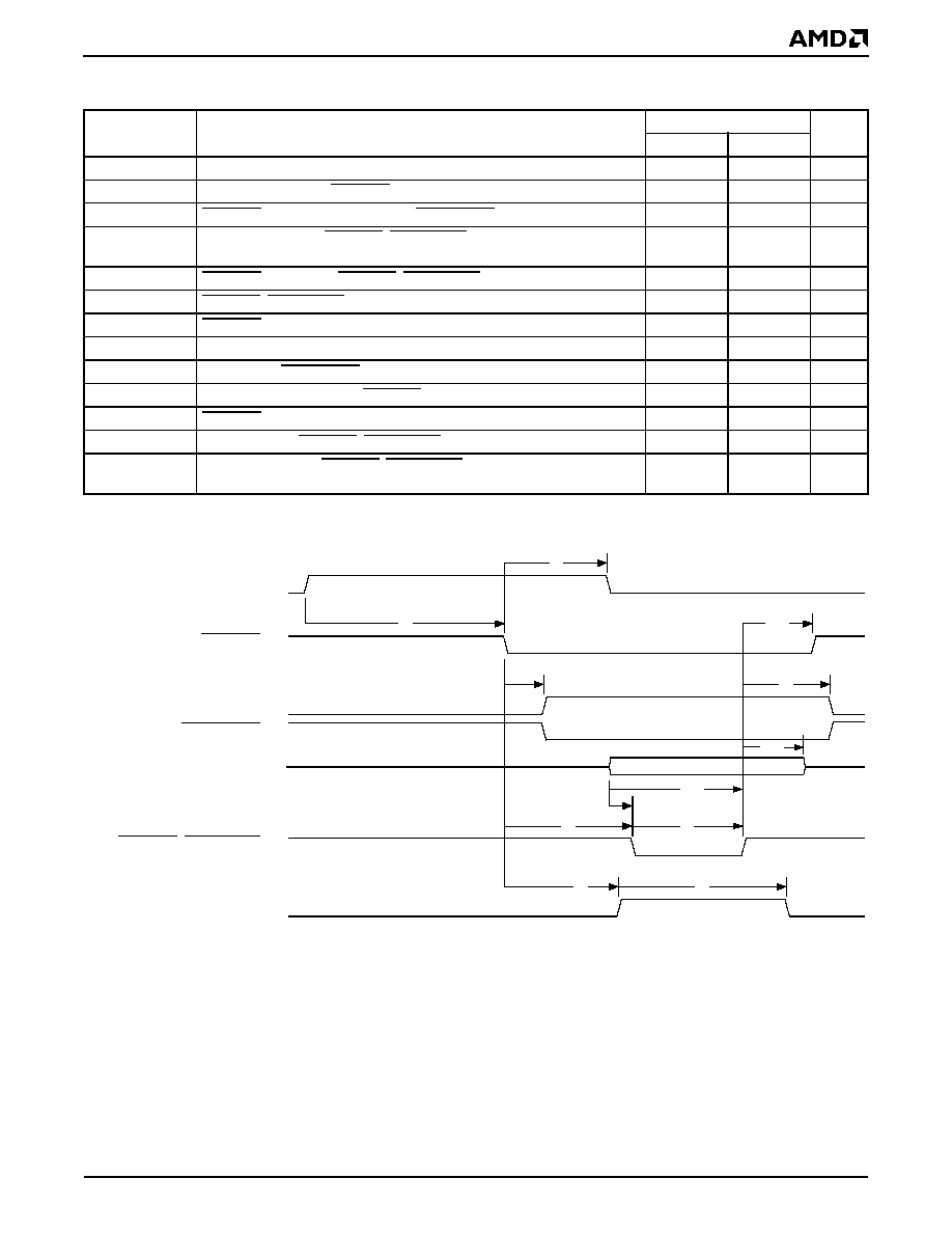
…lanTMSC520 Microcontroller Data Sheet
71
P R E L I M I N A R Y
Figure 37.
GP-DMA Read Cycle Timing
GP Bus DMA Read Cycle Timing
Symbol
Parameter Description
Advance Information
Unit
Min
Max
T
CLK
GP-DMA clock cycle
58
244
ns
t1
GPDRQ asserted to GPDACK assertion
2
--
T
CLK
t2
GPDACK asserted to GPAEN and GPDBUFOE assertion
1
--
T
CLK
t3
GPD setup time for GPIOWR, GPMEMWR for non-compressed and
non-extended write mode
20
--
ns
t4
GPDACK asserted to GPIOWR, GPMEMWR assertion
3.5
--
T
CLK
t5
GPIOWR, GPMEMWR pulse width
1
--
T
CLK
t6
GPDACK asserted to GPTC assertion
3.5
--
T
CLK
t7
GPTC pulse width
1.5
--
T
CLK
t8
GPAEN and GPDBUFOE deasserted from command deasserted
1
--
T
CLK
t9
GPDRQ deasserted from GPDACK assertion
0
--
ns
t10
GPDACK deasserted from command deasserted
1
--
T
CLK
t11
GPD hold from GPIOWR, GPMEMWR
0.5
--
T
CLK
t12
GPD setup time for GPIOWR, GPMEMWR for compressed or extended
write mode
0.5
--
T
CLK
t9
t1
t10
t2
t8
t11
t4
t3
t5
t6
t7
GPDRQ
GPDACK
GPAEN
GPD15≠GPD0
GPIOWR, GPMEMWR
GPTC
t12
GPDBUFOE

72
…lanTMSC520 Microcontroller Data Sheet
P R E L I M I N A R Y
Figure 38.
GP-DMA Write Cycle Timing
GP Bus DMA Write Cycle Timing
Symbol
Parameter Description
Advance Information
Unit
Min
Max
T
CLK
GP-DMA clock cycle
58
244
ns
t1
GPDRQ to GPDACK assertion
2
--
T
CLK
t2
GPDACK asserted to GPAEN and GPDBUFOE assertion
1
--
T
CLK
t3
GPIORD, GPMEMRD asserted to GPD valid
--
0.5
T
CLK
t4
GPDACK asserted to GPIORD, GPMEMRD assertion
2.5
--
T
CLK
t5
GPIORD, GPMEMRD pulse width
1.5
--
T
CLK
t6
GPDACK asserted to GPTC assertion
3.5
--
T
CLK
t7
GPTC pulse width
1.5
--
T
CLK
t8
GPAEN and GPDBUFOE deasserted from command deasserted
1
--
T
CLK
t9
GPDRQ deasserted from GPDACK assertion
0
--
ns
t10
GPDACK deasserted from command deasserted
1
--
T
CLK
t11
GPIORD, GPMEMRD deasserted to GPD invalid
0
--
ns
t9
t1
t10
t2
t8
t3
t11
t4
t5
t6
t7
GPDRQ
GPDACK
GPAEN
GPD15≠GPD0
GPIORD, GPMEMRD
GPTC
GPDBUFOE
…lanTMSC520 Microcontroller Data Sheet
73
P R E L I M I N A R Y
Figure 39.
SSI Timing
SSI Timing
Symbol
Parameter Description
Notes
Advance Information
Unit
Min
Max
t1
SSI_CLK period
1
Notes:
1. The clock period for the SSI interface is programmable as a divisor of the 33-MHz crystal input. Rates provided are binary
multiples from divide by 4 (~110 ns) to divide by 512 (~15526 ns). The actual period is affected by the frequency of the crystal
(33.000 MHz or 33.333 MHz).
110
--
ns
t2
SSI_CLK High time
55
--
ns
t3
SSI_CLK Low time
55
--
ns
t4
SSI_DI setup time to sample edge
2
2. The sample/assert clock edge for the SSI interface is programmable.
3
--
ns
t5
SSI_DI hold time from sample edge
2
3
--
ns
t6
SSI_DO hold time from assert edge
2
0
--
ns
t7
SSI_DO setup to sample edge
2,3
3. T
CLK
refers to the programmed period for the SSI_CLK pin.
(0.5 T
CLK
) ≠ 5
--
ns
t8
SSI_DO high impedance from sample edge of last bit
2,3
0.5 T
CLK
(0.5 T
CLK
) + 5
ns
t1
t2
t3
t7
t4
t5
t6
t6
t8
SSI_CLK
SSI_DI
SSI_DO
Notes:
Asserted on rising edge, sampled on falling edge.

74
…lanTMSC520 Microcontroller Data Sheet
P R E L I M I N A R Y
Figure 40.
JTAG Boundary Scan Timing
JTAG Timing
Symbol
Parameter Description
Advance Information
Unit
Min
Max
t1
JTAG_TRST active pulse width
20
--
ns
t2
JTAG_TCK period
40
--
ns
t3
JTAG_TCK High time
15
--
ns
t4
JTAG_TCK Low time
15
--
ns
t5
JTAG_TMS, JTAG_TDI setup time
5
--
ns
t6
JTAG_TMS, JTAG_TDI hold time
10
--
ns
t7
JTAG_TDO delay
--
10
ns
t8
Input pin setup time
15
--
ns
t9
Input pin hold time
15
--
ns
t10
Output pin delay
--
15
ns
t1
t2
t3
t4
t5
t6
t5
t6
t7
t8
t9
t10
JTAG_TRST
JTAG_TCK
JTAG_TMS
JTAG_TDI
JTAG_TDO
Input Pin
Output Pin

…lanTMSC520 Microcontroller Data Sheet
A-1
P R E L I M I N A R Y
APPENDIX A
PIN TABLES
This appendix contains pin tables for the …lanSC520
microcontroller. Several different tables are included
with the following characteristics:
s
Multiplexed signal tradeoffs--Table 16 on
page A-2.
s
Programmable I/O pins ordered by PIO pin number
and multiplexed signal name, respectively, including
a column showing pin configurations following
system reset--Table 17 on page A-4 and Table 18
on page A-5.
s
Pin summary showing signal name and alternate
function, pin number, I/O type, termination, reset
state, output drive, and maximum load--Table 20
on page A-7.
For pin tables showing pins sorted by pin number and
signal name, respectively, see "Pin Designations (Pin
Number)" on page 11 and "Pin Designations (Pin
Name)" on page 13.
For signal descriptions, see Table 2, "Signal Descrip-
tions" on page 17.
In all tables the brackets, [ ], indicate alternate, multi-
plexed functions, and braces, { }, indicate reset config-
uration pins (pinstraps). The line over a pin name
indicates an active Low signal. The word
pin
refers to
the physical wire; the word
signal
refers to the electrical
signal that flows through it.
A-2
…lanTMSC520 Microcontroller Data Sheet
P R E L I M I N A R Y
Table 16.
Multiplexed Signal Trade-Offs
Signal You Want
Signal You Give Up
Pin #
ROM/Flash Control
ROMCS1
GPCS1
B24
ROMCS2
GPCS2
C23
GP Bus
GPAEN
PIO3
AE11
GPALE
PIO0
AE12
GPBHE
PIO1
AF12
GPCS0
PIO27
AE4
GPCS1
ROMCS1
B24
GPCS2
ROMCS2
C23
GPCS3
PITGATE2
AC21
GPCS4
TMRIN1
AA24
GPCS5
TMRIN0
AC20
GPCS6
TMROUT1
AC23
GPCS7
TMROUT0
AD23
GPDACK0
PIO12
AC8
GPDACK1
PIO11
AC9
GPDACK2
PIO10
AD9
GPDACK3
PIO9
AE9
GPDBUFOE
PIO24
AD5
GPDRQ0
PIO8
AF9
GPDRQ1
PIO7
AF10
GPDRQ2
PIO6
AE10
GPDRQ3
PIO5
AD10
GPIOCS16
PIO25
AC4
GPIRQ0
PIO23
AE5
GPIRQ1
PIO22
AF5
GPIRQ2
PIO21
AF6
GPIRQ3
PIO20
AE6
GPIRQ4
PIO19
AD6
GPIRQ5
PIO18
AD7
GPIRQ6
PIO17
AE7
GPIRQ7
PIO16
AF7
GPIRQ8
PIO15
AF8
GPIRQ9
PIO14
AE8
GPIRQ10
PIO13
AD8
GPMEMCS16
PIO26
AD4
GPRDY
PIO2
AF11
GPTC
PIO4
AD11
Serial Ports
CTS2
PIO28
AF4
DCD2
PIO30
AE3
DSR2
PIO29
AF3
RIN2
PIO31
AD3
…lanTMSC520 Microcontroller Data Sheet
A-3
P R E L I M I N A R Y
Clocks
CLKTEST
CLKTIMER
A7
CLKTIMER
CLKTEST
A7
Timers
PITGATE2
GPCS3
AC21
TMRIN0
GPCS5
AC20
TMRIN1
GPCS4
AA24
TMROUT0
GPCS7
AD23
TMROUT1
GPCS6
AC23
System Test
CF_DRAM
WBMSTR2
W24
CF_ROM_GPCS
WBMSTR0
AD20
DATASTRB
WBMSTR1
AC24
WBMSTR0
CF_ROM_GPCS
AD20
WBMSTR1
DATASTRB
AC24
WBMSTR2
CF_DRAM
W24
Configuration Pins (Pinstraps)--See "Configuration" on
page 26.
Programmable I/O
PIO0
GPALE
AE12
PIO1
GPBHE
AF12
PIO2
GPRDY
AF11
PIO3
GPAEN
AE11
PIO4
GPTC
AD11
PIO5
GPDRQ3
AD10
PIO6
GPDRQ2
AE10
PIO7
GPDRQ1
AF10
PIO8
GPDRQ0
AF9
PIO9
GPDACK3
AE9
PIO10
GPDACK2
AD9
PIO11
GPDACK1
AC9
PIO12
GPDACK0
AC8
PIO13
GPIRQ10
AD8
PIO14
GPIRQ9
AE8
PIO15
GPIRQ8
AF8
PIO16
GPIRQ7
AF7
PIO17
GPIRQ6
AE7
PIO18
GPIRQ5
AD7
PIO19
GPIRQ4
AD6
PIO20
GPIRQ3
AE6
PIO21
GPIRQ2
AF6
PIO22
GPIRQ1
AF5
PIO23
GPIRQ0
AE5
PIO24
GPDBUFOE
AD5
PIO25
GPIOCS16
AC4
PIO26
GPMEMCS16
AD4
PIO27
GPCS0
AE4
Table 16.
Multiplexed Signal Trade-Offs (Continued)
Signal You Want
Signal You Give Up
Pin #
A-4
…lanTMSC520 Microcontroller Data Sheet
P R E L I M I N A R Y
Table 17.
PIOs Sorted by PIO Number
PIO (Default
Function)
Pin #
Multiplexed
Signal
Pin Configuration
Following System Reset
PIO0
AE12
GPALE
Input with pullup
PIO1
AF12
GPBHE
Input with pullup
PIO2
AF11
GPRDY
Input with pullup
PIO3
AE11
GPAEN
Input with pullup
PIO4
AD11
GPTC
Input with pullup
PIO5
AD10
GPDRQ3
Input with pulldown
PIO6
AE10
GPDRQ2
Input with pulldown
PIO7
AF10
GPDRQ1
Input with pulldown
PIO8
AF9
GPDRQ0
Input with pulldown
PIO9
AE9
GPDACK3
Input with pullup
PIO10
AD9
GPDACK2
Input with pullup
PIO11
AC9
GPDACK1
Input with pullup
PIO12
AC8
GPDACK0
Input with pullup
PIO13
AD8
GPIRQ10
Input with pullup
PIO14
AE8
GPIRQ9
Input with pullup
PIO15
AF8
GPIRQ8
Input with pullup
PIO16
AF7
GPIRQ7
Input with pullup
PIO17
AE7
GPIRQ6
Input with pullup
PIO18
AD7
GPIRQ5
Input with pullup
PIO19
AD6
GPIRQ4
Input with pullup
PIO20
AE6
GPIRQ3
Input with pullup
PIO21
AF6
GPIRQ2
Input with pullup
PIO22
AF5
GPIRQ1
Input with pullup
PIO23
AE5
GPIRQ0
Input with pullup
PIO24
AD5
GPDBUFOE
Input with pullup
PIO25
AC4
GPIOCS16
Input with pullup
PIO26
AD4
GPMEMCS16
Input with pullup
PIO27
AE4
GPCS0
Input with pullup
PIO28
AF4
CTS2
Input with pullup
PIO29
AF3
DSR2
Input with pullup
PIO30
AE3
DCD2
Input with pullup
PIO31
AD3
RIN2
Input with pullup

…lanTMSC520 Microcontroller Data Sheet
A-5
P R E L I M I N A R Y
Table 18.
PIOs Sorted by Signal Name
Multiplexed
Signal
PIO (Default
Function)
Pin Configuration
Following System Reset
Pin #
CTS2
PIO28
Input with pullup
AF4
DCD2
PIO30
Input with pullup
AE3
DSR2
PIO29
Input with pullup
AF3
GPAEN
PIO3
Input with pullup
AE11
GPALE
PIO0
Input with pullup
AE12
GPBHE
PIO1
Input with pullup
AF12
GPCS0
PIO27
Input with pullup
AE4
GPDACK0
PIO12
Input with pullup
AC8
GPDACK1
PIO11
Input with pullup
AC9
GPDACK2
PIO10
Input with pullup
AD9
GPDACK3
PIO9
Input with pullup
AE9
GPDBUFOE
PIO24
Input with pullup
AD5
GPDRQ0
PIO8
Input with pulldown
AF9
GPDRQ1
PIO7
Input with pulldown
AF10
GPDRQ2
PIO6
Input with pulldown
AE10
GPDRQ3
PIO5
Input with pulldown
AD10
GPIOCS16
PIO25
Input with pullup
AC4
GPIRQ0
PIO23
Input with pullup
AE5
GPIRQ1
PIO22
Input with pullup
AF5
GPIRQ10
PIO13
Input with pullup
AD8
GPIRQ2
PIO21
Input with pullup
AF6
GPIRQ3
PIO20
Input with pullup
AE6
GPIRQ4
PIO19
Input with pullup
AD6
GPIRQ5
PIO18
Input with pullup
AD7
GPIRQ6
PIO17
Input with pullup
AE7
GPIRQ7
PIO16
Input with pullup
AF7
GPIRQ8
PIO15
Input with pullup
AF8
GPIRQ9
PIO14
Input with pullup
AE8
GPMEMCS16
PIO26
Input with pullup
AD4
GPRDY
PIO2
Input with pullup
AF11
GPTC
PIO4
Input with pullup
AD11
RIN2
PIO31
Input with pullup
AD3
A-6
…lanTMSC520 Microcontroller Data Sheet
P R E L I M I N A R Y
Pin List Summary Table Column Definitions
The following paragraphs describe the individual columns
of information in Table 20, "Pin List Summary," on page
A-7. The pins are grouped alphabetically by function.
Column #1--Signal Name, [Alternate Function],
{Pinstrap}
This column denotes the primary and alternate func-
tions of the pins.
Brackets, [ ], are used to indicate the alternate, multi-
plexed function of a pin.
Braces, { }, are used to indicate the functionality of a pin
only during a processor reset. These signals are called
pinstraps. For pinstraps, see "Configuration" on
page 26.
Column #2--Pin #
The pin number column identifies the pin number of the
individual I/O signal on the package.
Column #3--Type
Definitions of the abbreviations in the Type column are
shown in Table 19.
Column #4--Termination
The Termination column specifies the presence of
pullups or pulldowns on the pins.
Column #5--Reset State
Definitions of the abbreviations in the Reset State col-
umn are shown in Table 19.
Column #6--Output Drive
The Output Drive column shows the output amperage.
Column #7--Max Load (pF)
The Max Load column designates the capacitive load
at which the I/O timing for that pin is guaranteed.
Column #8--Note
The Note column shows footnote numbers.
Table 19.
Pin List Summary Table Abbreviations
Type
Definition
--
None or not applicable.
[ ]
Brackets signify a programmable alternate state.
{ }
Reset configuration pin. These are the
configuration pins latched during reset.
Active
Used in the Reset State column to indicate
signals active during reset.
Analog
Pin is an analog input.
B
Bidirectional.
H
Driven High (a logical 1).
I
Pin is an input.
IOD
Input or open-drain output.
L
Driven Low (a logical 0).
Latched
Used in the Reset State column to indicate a
signal latched on reset.
NA
Not applicable.
O
Pin is an active output.
OD
Open-drain output.
Osc
Oscillator.
PD
Built-in pulldown resistor (~100≠150 k
W).
Power
Power pins.
PU
Built-in pullup resistor (~100≠150 k
W).
STI
Pin is a Schmitt trigger input.
STS
Sustained three-state (PCI drive).
TS
Three-state output.

…lanTMSC520 Microcontroller Data Sheet
A-7
P R E L I M I N A R Y
Table 20.
Pin List Summary
Signal Name
[Alternate Function]
{Pinstrap}
Pin #
Type
Termination
Reset
State
Output
Drive
Max Load
(pF)
SDRAM
BA0
T25
O
--
H
12/18/24 mA
50 pF
BA1
U25
O
--
H
12/18/24 mA
50 pF
CLKMEMIN
A4
I
--
I
--
--
CLKMEMOUT
B19
O
--
Active
24 mA
50 pF
MA0
L25
O
--
H
12/18/24 mA
50 pF
MA1
L26
O
--
H
12/18/24 mA
50 pF
MA2
M26
O
--
H
12/18/24 mA
50 pF
MA3
M25
O
--
H
12/18/24 mA
50 pF
MA4
N25
O
--
H
12/18/24 mA
50 pF
MA5
N26
O
--
H
12/18/24 mA
50 pF
MA6
P26
O
--
H
12/18/24 mA
50 pF
MA7
P25
O
--
H
12/18/24 mA
50 pF
MA8
R25
O
--
H
12/18/24 mA
50 pF
MA9
R26
O
--
H
12/18/24 mA
50 pF
MA10
T26
O
--
H
12/18/24 mA
50 pF
MA11
U26
O
--
H
12/18/24 mA
50 pF
MA12
V26
O
--
H
12/18/24 mA
50 pF
MD0
B7
B
--
I
12/18/24 mA
50 pF
MD1
A8
B
--
I
12/18/24 mA
50 pF
MD2
B9
B
--
I
12/18/24 mA
50 pF
MD3
A10
B
--
I
12/18/24 mA
50 pF
MD4
B11
B
--
I
12/18/24 mA
50 pF
MD5
A12
B
--
I
12/18/24 mA
50 pF
MD6
B13
B
--
I
12/18/24 mA
50 pF
MD7
A14
B
--
I
12/18/24 mA
50 pF
MD8
B15
B
--
I
12/18/24 mA
50 pF
MD9
A16
B
--
I
12/18/24 mA
50 pF
MD10
B17
B
--
I
12/18/24 mA
50 pF
MD11
A18
B
--
I
12/18/24 mA
50 pF
MD12
B20
B
--
I
12/18/24 mA
50 pF
MD13
A21
B
--
I
12/18/24 mA
50 pF
MD14
A22
B
--
I
12/18/24 mA
50 pF
MD15
B23
B
--
I
12/18/24 mA
50 pF
MD16
B8
B
--
I
12/18/24 mA
50 pF
MD17
A9
B
--
I
12/18/24 mA
50 pF
MD18
B10
B
--
I
12/18/24 mA
50 pF
MD19
A11
B
--
I
12/18/24 mA
50 pF
MD20
B12
B
--
I
12/18/24 mA
50 pF
MD21
A13
B
--
I
12/18/24 mA
50 pF
MD22
B14
B
--
I
12/18/24 mA
50 pF
MD23
A15
B
--
I
12/18/24 mA
50 pF
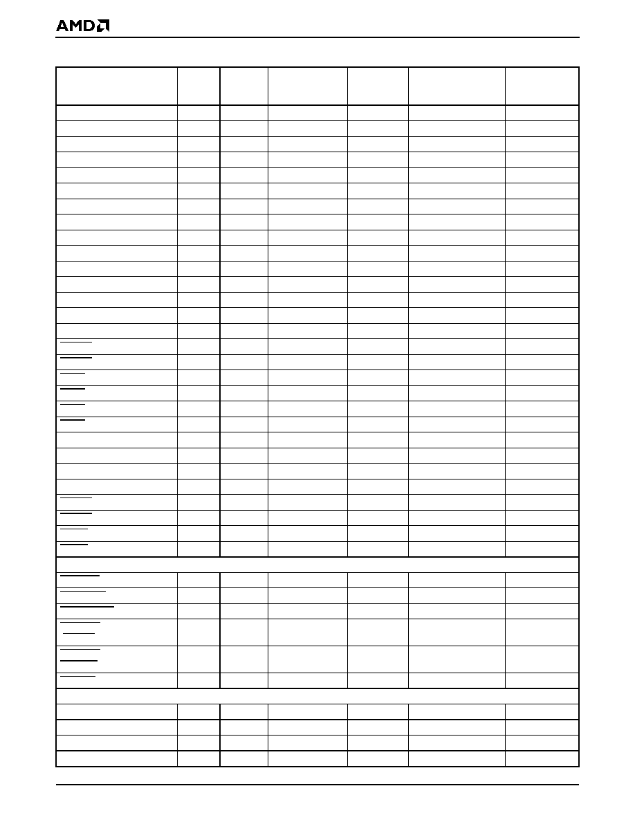
A-8
…lanTMSC520 Microcontroller Data Sheet
P R E L I M I N A R Y
MD24
B16
B
--
I
12/18/24 mA
50 pF
MD25
A17
B
--
I
12/18/24 mA
50 pF
MD26
B18
B
--
I
12/18/24 mA
50 pF
MD27
A19
B
--
I
12/18/24 mA
50 pF
MD28
A20
B
--
I
12/18/24 mA
50 pF
MD29
B21
B
--
I
12/18/24 mA
50 pF
MD30
A23
B
--
I
12/18/24 mA
50 pF
MD31
A24
B
--
I
12/18/24 mA
50 pF
MECC0
C25
B
--
I
12/18/24 mA
50 pF
MECC1
D26
B
--
I
12/18/24 mA
50 pF
MECC2
W26
B
--
I
12/18/24 mA
50 pF
MECC3
Y25
B
--
I
12/18/24 mA
50 pF
MECC4
C26
B
--
I
12/18/24 mA
50 pF
MECC5
D25
B
--
I
12/18/24 mA
50 pF
MECC6
Y26
B
--
I
12/18/24 mA
50 pF
SCASA
F25
O
--
H
12/18/24 mA
50 pF
SCASB
F26
O
--
H
12/18/24 mA
50 pF
SCS0
V25
O
--
H
12/18 mA
50 pF
SCS1
W25
O
--
H
12/18 mA
50 pF
SCS2
J25
O
--
H
12/18 mA
50 pF
SCS3
J26
O
--
H
12/18 mA
50 pF
SDQM0
G25
O
--
H
12/18/24 mA
50 pF
SDQM1
H26
O
--
H
12/18/24 mA
50 pF
SDQM2
G26
O
--
H
12/18/24 mA
50 pF
SDQM3
H25
O
--
H
12/18/24 mA
50 pF
SRASA
K25
O
--
H
12/18/24 mA
50 pF
SRASB
K26
O
--
H
12/18/24 mA
50 pF
SWEA
E26
O
--
H
12/18/24 mA
50 pF
SWEB
E25
O
--
H
12/18/24 mA
50 pF
ROM/Flash Control
BOOTCS
AB25
O
--
H
12 mA
70 pF
FLASHWR
AB24
O
--
H
24 mA
70 pF
ROMBUFOE
AA25
O
--
H
12 mA
70 pF
ROMCS1
[GPCS1]
B24
O
[O]
--
H
12 mA
70 pF
ROMCS2
[GPCS2]
C23
O
[O]
--
H
12 mA
70 pF
ROMRD
AB23
O
--
H
24 mA
70 pF
PCI Bus
AD0
AC2
STS-B
--
L
--
--
AD1
AC1
STS-B
--
L
--
--
AD2
AB1
STS-B
--
L
--
--
AD3
AB2
STS-B
--
L
--
--
Table 20.
Pin List Summary (Continued)
Signal Name
[Alternate Function]
{Pinstrap}
Pin #
Type
Termination
Reset
State
Output
Drive
Max Load
(pF)
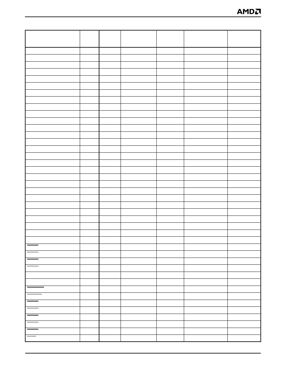
…lanTMSC520 Microcontroller Data Sheet
A-9
P R E L I M I N A R Y
AD4
AA2
STS-B
--
L
--
--
AD5
AA1
STS-B
--
L
--
--
AD6
Y1
STS-B
--
L
--
--
AD7
Y2
STS-B
--
L
--
--
AD8
W1
STS-B
--
L
--
--
AD9
V1
STS-B
--
L
--
--
AD10
V2
STS-B
--
L
--
--
AD11
U2
STS-B
--
L
--
--
AD12
U1
STS-B
--
L
--
--
AD13
T1
STS-B
--
L
--
--
AD14
T2
STS-B
--
L
--
--
AD15
R2
STS-B
--
L
--
--
AD16
K2
STS-B
--
L
--
--
AD17
J2
STS-B
--
L
--
--
AD18
J1
STS-B
--
L
--
--
AD19
H1
STS-B
--
L
--
--
AD20
H2
STS-B
--
L
--
--
AD21
G2
STS-B
--
L
--
--
AD22
G1
STS-B
--
L
--
--
AD23
F1
STS-B
--
L
--
--
AD24
E2
STS-B
--
L
--
--
AD25
E1
STS-B
--
L
--
--
AD26
D1
STS-B
--
L
--
--
AD27
D2
STS-B
--
L
--
--
AD28
B2
STS-B
--
L
--
--
AD29
B1
STS-B
--
L
--
--
AD30
A1
STS-B
--
L
--
--
AD31
A2
STS-B
--
L
--
--
CBE0
W2
STS-B
--
L
--
--
CBE1
R1
STS-B
--
L
--
--
CBE2
K1
STS-B
--
L
--
--
CBE3
F2
STS-B
--
L
--
--
CLKPCIIN
G3
I
--
I
--
--
CLKPCIOUT
A6
O
--
Active
--
--
DEVSEL
M1
STS-B
--
TS
--
--
FRAME
L1
STS-B
--
TS
--
--
GNT0
M3
O
--
TS
--
--
GNT1
N4
O
--
TS
--
--
GNT2
P3
O
--
TS
--
--
GNT3
T3
O
--
TS
--
--
GNT4
U4
O
--
TS
--
--
INTA
K3
I
--
I
--
--
Table 20.
Pin List Summary (Continued)
Signal Name
[Alternate Function]
{Pinstrap}
Pin #
Type
Termination
Reset
State
Output
Drive
Max Load
(pF)
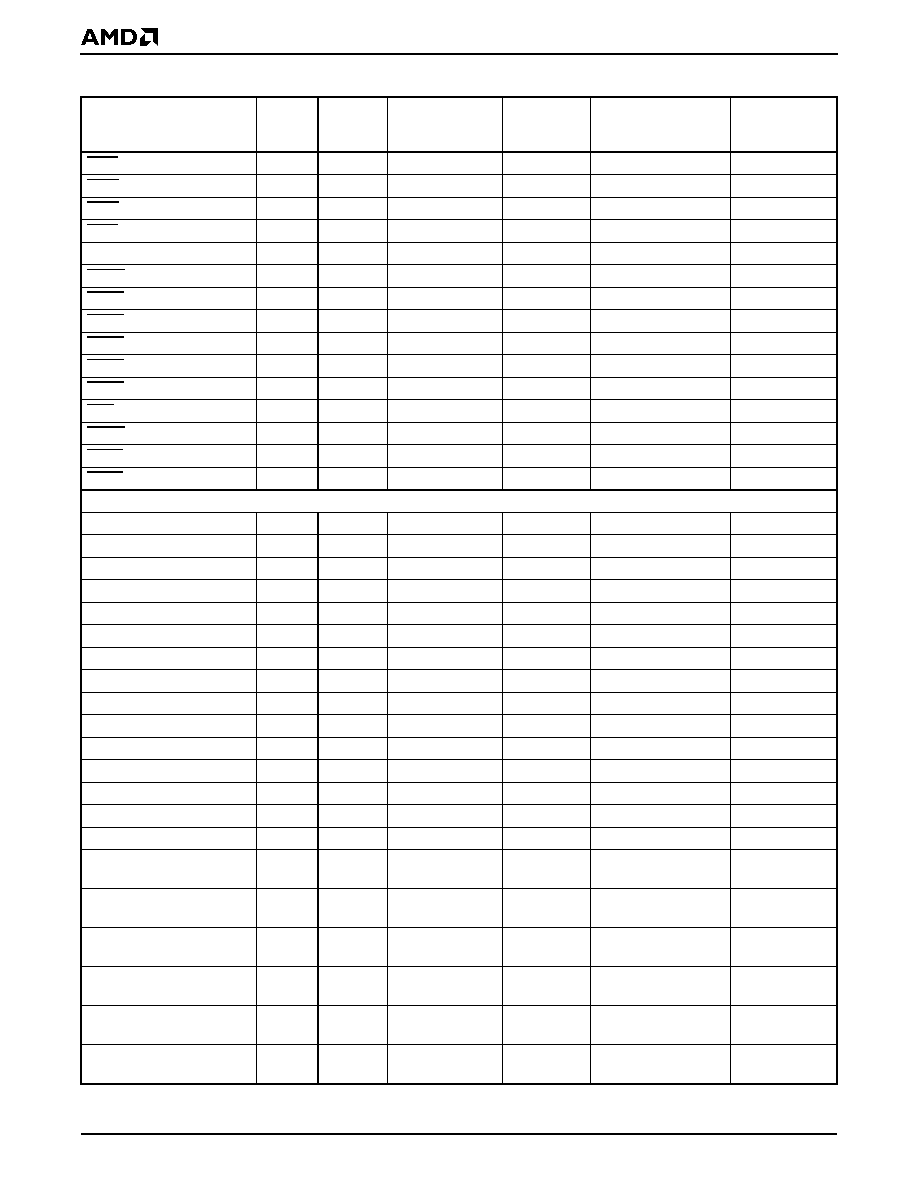
A-10
…lanTMSC520 Microcontroller Data Sheet
P R E L I M I N A R Y
INTB
J3
I
--
I
--
--
INTC
H3
I
--
I
--
--
INTD
H4
I
--
I
--
--
IRDY
L2
STS-B
--
TS
--
--
PAR
P1
STS-B
--
L
--
--
PERR
N2
STS-B
--
TS
--
--
REQ0
L3
I
--
I
--
--
REQ1
N3
I
--
I
--
--
REQ2
P4
I
--
I
--
--
REQ3
R3
I
--
I
--
--
REQ4
U3
I
--
I
--
--
RST
A5
O
--
L
--
--
SERR
P2
STS-I
--
TS
--
--
STOP
N1
STS-B
--
TS
--
--
TRDY
M2
STS-B
--
TS
--
--
GP Bus
GPA0
J24
O
--
H
12 mA
70 pF
GPA1
G4
O
--
H
12 mA
70 pF
GPA2
K24
O
--
H
12 mA
70 pF
GPA3
J23
O
--
H
12 mA
70 pF
GPA4
L24
O
--
H
12 mA
70 pF
GPA5
H24
O
--
H
12 mA
70 pF
GPA6
C1
O
--
H
12 mA
70 pF
GPA7
F23
O
--
H
12 mA
70 pF
GPA8
M24
O
--
H
12 mA
70 pF
GPA9
C2
O
--
H
12 mA
70 pF
GPA10
M23
O
--
H
12 mA
70 pF
GPA11
N23
O
--
H
12 mA
70 pF
GPA12
N24
O
--
H
12 mA
70 pF
GPA13
P24
O
--
H
12 mA
70 pF
GPA14
R24
O
--
H
12 mA
70 pF
GPA15
{RSTLD0}
C24
O
{I}
PD
Latched
12 mA
70 pF
GPA16
{RSTLD1}
D24
O
{I}
PD
Latched
12 mA
70 pF
GPA17
{RSTLD2}
E24
O
{I}
PD
Latched
12 mA
70 pF
GPA18
{RSTLD3}
B22
O
{I}
PD
Latched
12 mA
70 pF
GPA19
{RSTLD4}
C21
O
{I}
PD
Latched
12 mA
70 pF
GPA20
{RSTLD5}
C14
O
{I}
PD
Latched
12 mA
70 pF
Table 20.
Pin List Summary (Continued)
Signal Name
[Alternate Function]
{Pinstrap}
Pin #
Type
Termination
Reset
State
Output
Drive
Max Load
(pF)
…lanTMSC520 Microcontroller Data Sheet
A-11
P R E L I M I N A R Y
GPA21
{RSTLD6}
C19
O
{I}
PD
Latched
12 mA
70 pF
GPA22
{RSTLD7}
F3
O
{I}
PD
Latched
12 mA
70 pF
GPA23
{AMDEBUG_DIS}
D3
O
{I}
PD
Latched
12 mA
70 pF
GPA24
{INST_TRCE}
D4
O
{I}
PD
Latched
12 mA
70 pF
GPA25
{DEBUG_ENTER}
C3
O
{I}
PD
Latched
12 mA
70 pF
GPD0
C4
B
PU
I
12 mA
70 pF
GPD1
B5
B
PU
I
12 mA
70 pF
GPD2
C7
B
PU
I
12 mA
70 pF
GPD3
C8
B
PU
I
12 mA
70 pF
GPD4
C9
B
PU
I
12 mA
70 pF
GPD5
D9
B
PU
I
12 mA
70 pF
GPD6
D10
B
PU
I
12 mA
70 pF
GPD7
C10
B
PU
I
12 mA
70 pF
GPD8
C11
B
PU
I
12 mA
70 pF
GPD9
C12
B
PU
I
12 mA
70 pF
GPD10
C13
B
PU
I
12 mA
70 pF
GPD11
D13
B
PU
I
12 mA
70 pF
GPD12
D14
B
PU
I
12 mA
70 pF
GPD13
C15
B
PU
I
12 mA
70 pF
GPD14
C17
B
PU
I
12 mA
70 pF
GPD15
D17
B
PU
I
12 mA
70 pF
GPIORD
G24
O
--
H
12 mA
70 pF
GPIOWR
C16
O
--
H
12 mA
70 pF
GPMEMRD
F24
O
--
H
12 mA
70 pF
GPMEMWR
C18
O
--
H
12 mA
70 pF
GPRESET
AC22
O
--
H
6 mA
70 pF
PIO0
[GPALE]
AE12
B
[O]
PU
I
6 mA
30 pF
PIO1
[GPBHE]
AF12
B
[O]
PU
I
6 mA
30 pF
PIO2
[GPRDY]
AF11
B
[STI]
PU
I
6 mA
30 pF
PIO3
[GPAEN]
AE11
B
[O]
PU
I
6 mA
30 pF
PIO4
[GPTC]
AD11
B
[O]
PU
I
6 mA
30 pF
PIO5
[GPDRQ3]
AD10
B
[I]
PD
I
6 mA
30 pF
PIO6
[GPDRQ2]
AE10
B
[I]
PD
I
6 mA
30 pF
Table 20.
Pin List Summary (Continued)
Signal Name
[Alternate Function]
{Pinstrap}
Pin #
Type
Termination
Reset
State
Output
Drive
Max Load
(pF)
A-12
…lanTMSC520 Microcontroller Data Sheet
P R E L I M I N A R Y
PIO7
[GPDRQ1]
AF10
B
[I]
PD
I
6 mA
30 pF
PIO8
[GPDRQ0]
AF9
B
[I]
PD
I
6 mA
30 pF
PIO9
[GPDACK3]
AE9
B
[O]
PU
I
6 mA
30 pF
PIO10
[GPDACK2]
AD9
B
[O]
PU
I
6 mA
30 pF
PIO11
[GPDACK1]
AC9
B
[O]
PU
I
6 mA
30 pF
PIO12
[GPDACK0]
AC8
B
[O]
PU
I
6 mA
30 pF
PIO13
[GPIRQ10]
AD8
B
[I]
PU
I
6 mA
30 pF
PIO14
[GPIRQ9]
AE8
B
[I]
PU
I
6 mA
30 pF
PIO15
[GPIRQ8]
AF8
B
[I]
PU
I
6 mA
30 pF
PIO16
[GPIRQ7]
AF7
B
[I]
PU
I
6 mA
30 pF
PIO17
[GPIRQ6]
AE7
B
[I]
PU
I
6 mA
30 pF
PIO18
[GPIRQ5]
AD7
B
[I]
PU
I
6 mA
30 pF
PIO19
[GPIRQ4]
AD6
B
[I]
PU
I
6 mA
30 pF
PIO20
[GPIRQ3]
AE6
B
[I]
PU
I
6 mA
30 pF
PIO21
[GPIRQ2]
AF6
B
[I]
PU
I
6 mA
30 pF
PIO22
[GPIRQ1]
AF5
B
[I]
PU
I
6 mA
30 pF
PIO23
[GPIRQ0]
AE5
B
[I]
PU
I
6 mA
30 pF
PIO24
[GPDBUFOE]
AD5
B
[O]
PU
I
6 mA
30 pF
PIO25
[GPIOCS16]
AC4
B
[STI]
PU
I
6 mA
30 pF
PIO26
[GPMEMCS16]
AD4
B
[STI]
PU
I
6 mA
30 pF
PIO27
[GPCS0]
AE4
B
[O]
PU
I
6 mA
30 pF
Serial Ports
CTS1
V3
I
PU
I
--
--
DCD1
V4
I
PU
I
--
--
DSR1
Y3
I
PU
I
--
--
DTR1
W3
O
--
H
6 mA
30 pF
DTR2
AE23
O
--
H
6 mA
30 pF
Table 20.
Pin List Summary (Continued)
Signal Name
[Alternate Function]
{Pinstrap}
Pin #
Type
Termination
Reset
State
Output
Drive
Max Load
(pF)
…lanTMSC520 Microcontroller Data Sheet
A-13
P R E L I M I N A R Y
PIO28
[CTS2]
AF4
B
[I]
PU
I
6 mA
30 pF
PIO29
[DSR2]
AF3
B
[I]
PU
I
6 mA
30 pF
PIO30
[DCD2]
AE3
B
[I]
PU
I
6 mA
30 pF
PIO31
[RIN2]
AD3
B
[I]
PU
I
6 mA
30 pF
RIN1
AA3
I
PU
I
--
--
RTS1
W4
O
--
H
6 mA
30 pF
RTS2
AD22
O
--
H
6 mA
30 pF
SIN1
AE2
I
PU
I
--
--
SIN2
V24
I
PU
I
--
--
SOUT1
AF2
O
--
H
6 mA
30 pF
SOUT2
U23
O
--
H
6 mA
30 pF
SSI_CLK
AD19
O
--
H
6 mA
30 pF
SSI_DI
AE19
STI
PU
I
--
--
SSI_DO
AF19
OD
--
L
6 mA
30 pF
Clocks and Reset
32KXTAL1
AF26
Osc
--
Active
--
--
32KXTAL2
AE26
Osc
--
Active
--
--
33MXTAL1
AB26
Osc
--
Active
--
--
33MXTAL2
AC26
Osc
--
Active
--
--
CLKTIMER
[CLKTEST]
A7
I
[O]
PU
I
18 mA
50 pF
LF_PLL1
AF24
Osc
--
Active
--
--
PRGRESET
D20
STI
--
I
--
--
PWRGOOD
C20
STI
--
I
--
--
JTAG
JTAG_TCK
AD21
I
PU
I
--
--
JTAG_TDI
AF21
I
PU
I
--
--
JTAG_TDO
AF22
O/TS
PU
TS
6 mA
30 pF
JTAG_TMS
AE21
I
PU
I
--
--
JTAG_TRST
AE22
I
PD
I
--
--
AMDebug Interface
BR/TC
AD24
I
PD
I
--
--
CMDACK
U24
O
--
L
6 mA
30 pF
STOP/TX
AF17
O
--
L
6 mA
30 pF
TRIG/TRACE
AC13
O
--
L
6 mA
30 pF
System Test
CF_DRAM
[WBMSTR2]
{CFG2}
W24
O
[O]
{I}
PD
Latched
6 mA
30 pF
Table 20.
Pin List Summary (Continued)
Signal Name
[Alternate Function]
{Pinstrap}
Pin #
Type
Termination
Reset
State
Output
Drive
Max Load
(pF)
A-14
…lanTMSC520 Microcontroller Data Sheet
P R E L I M I N A R Y
CF_ROM_GPCS
[WBMSTR0]
{CFG0}
AD20
O
[O]
{I}
PD
Latched
6 mA
30 pF
DATASTRB
[WBMSTR1]
{CFG1}
AC24
O
[O]
{I}
PD
Latched
6 mA
30 pF
Timers
PITGATE2
[GPCS3]
AC21
I
[O]
PU
I
6 mA
30 pF
PITOUT2
{CFG3}
Y24
O
{I}
PD
Latched
6 mA
30 pF
TMRIN0
[GPCS5]
AC20
I
[O]
PU
I
6 mA
30 pF
TMRIN1
[GPCS4]
AA24
I
[O]
PU
I
6 mA
30 pF
TMROUT0
[GPCS7]
AD23
O
[O]
--
H
6 mA
30 pF
TMROUT1
[GPCS6]
AC23
O
[O]
--
H
6 mA
30 pF
Power and Ground
BBATSEN
B25
Analog
--
Latched
--
--
GND
L11
Power
--
--
--
--
GND
L12
Power
--
--
--
--
GND
L13
Power
--
--
--
--
GND
L14
Power
--
--
--
--
GND
L15
Power
--
--
--
--
GND
L16
Power
--
--
--
--
GND
M11
Power
--
--
--
--
GND
M12
Power
--
--
--
--
GND
M13
Power
--
--
--
--
GND
M14
Power
--
--
--
--
GND
M15
Power
--
--
--
--
GND
M16
Power
--
--
--
--
GND
N11
Power
--
--
--
--
GND
N12
Power
--
--
--
--
GND
N13
Power
--
--
--
--
GND
N14
Power
--
--
--
--
GND
N15
Power
--
--
--
--
GND
N16
Power
--
--
--
--
GND
P11
Power
--
--
--
--
GND
P12
Power
--
--
--
--
GND
P13
Power
--
--
--
--
GND
P14
Power
--
--
--
--
GND
P15
Power
--
--
--
--
GND
P16
Power
--
--
--
--
Table 20.
Pin List Summary (Continued)
Signal Name
[Alternate Function]
{Pinstrap}
Pin #
Type
Termination
Reset
State
Output
Drive
Max Load
(pF)
…lanTMSC520 Microcontroller Data Sheet
A-15
P R E L I M I N A R Y
GND
R11
Power
--
--
--
--
GND
R12
Power
--
--
--
--
GND
R13
Power
--
--
--
--
GND
R14
Power
--
--
--
--
GND
R15
Power
--
--
--
--
GND
R16
Power
--
--
--
--
GND
T11
Power
--
--
--
--
GND
T12
Power
--
--
--
--
GND
T13
Power
--
--
--
--
GND
T14
Power
--
--
--
--
GND
T15
Power
--
--
--
--
GND
T16
Power
--
--
--
--
GND_ANLG
A25
Power
--
--
--
--
VCC_ANLG
B26
Power
--
--
--
--
VCC_CORE
AC14
Power
--
--
--
--
VCC_CORE
AC15
Power
--
--
--
--
VCC_CORE
AC5
Power
--
--
--
--
VCC_CORE
AC6
Power
--
--
--
--
VCC_CORE
AC7
Power
--
--
--
--
VCC_CORE
D11
Power
--
--
--
--
VCC_CORE
D12
Power
--
--
--
--
VCC_CORE
D18
Power
--
--
--
--
VCC_CORE
D19
Power
--
--
--
--
VCC_CORE
E4
Power
--
--
--
--
VCC_CORE
F4
Power
--
--
--
--
VCC_CORE
G23
Power
--
--
--
--
VCC_CORE
H23
Power
--
--
--
--
VCC_CORE
P23
Power
--
--
--
--
VCC_CORE
R23
Power
--
--
--
--
VCC_CORE
R4
Power
--
--
--
--
VCC_CORE
T4
Power
--
--
--
--
VCC_I/O
AA23
Power
--
--
--
--
VCC_I/O
AA4
Power
--
--
--
--
VCC_I/O
AC10
Power
--
--
--
--
VCC_I/O
AC11
Power
--
--
--
--
VCC_I/O
AC18
Power
--
--
--
--
VCC_I/O
AC19
Power
--
--
--
--
VCC_I/O
D15
Power
--
--
--
--
VCC_I/O
D16
Power
--
--
--
--
VCC_I/O
D21
Power
--
--
--
--
VCC_I/O
D22
Power
--
--
--
--
VCC_I/O
D5
Power
--
--
--
--
Table 20.
Pin List Summary (Continued)
Signal Name
[Alternate Function]
{Pinstrap}
Pin #
Type
Termination
Reset
State
Output
Drive
Max Load
(pF)

A-16
…lanTMSC520 Microcontroller Data Sheet
P R E L I M I N A R Y
VCC_I/O
D6
Power
--
--
--
--
VCC_I/O
D7
Power
--
--
--
--
VCC_I/O
D8
Power
--
--
--
--
VCC_I/O
J4
Power
--
--
--
--
VCC_I/O
K23
Power
--
--
--
--
VCC_I/O
K4
Power
--
--
--
--
VCC_I/O
L23
Power
--
--
--
--
VCC_I/O
L4
Power
--
--
--
--
VCC_I/O
M4
Power
--
--
--
--
VCC_I/O
V23
Power
--
--
--
--
VCC_I/O
W23
Power
--
--
--
--
VCC_I/O
Y23
Power
--
--
--
--
VCC_I/O
Y4
Power
--
--
--
--
VCC_RTC
A26
Power
--
--
--
--
No Connects
1
NC
A3
--
--
--
--
--
NC
AA26
--
--
--
--
--
NC
AB3
--
--
--
--
--
NC
AB4
--
--
--
--
--
NC
AC12
--
--
--
--
--
NC
AC16
--
--
--
--
--
NC
AC17
--
--
--
--
--
NC
AC25
--
--
--
--
--
NC
AC3
--
--
--
--
--
NC
AD1
--
--
--
--
--
NC
AD12
--
--
--
--
--
NC
AD13
--
--
--
--
--
NC
AD14
--
--
--
--
--
NC
AD15
--
--
--
--
--
NC
AD16
--
--
--
--
--
NC
AD17
--
--
--
--
--
NC
AD18
--
--
--
--
--
NC
AD2
--
--
--
--
--
NC
AD25
--
--
--
--
--
NC
AD26
--
--
--
--
--
NC
AE1
--
--
--
--
--
NC
AE13
--
--
--
--
--
NC
AE14
--
--
--
--
--
NC
AE15
--
--
--
--
--
NC
AE16
--
--
--
--
--
NC
AE17
--
--
--
--
--
NC
AE18
--
--
--
--
--
Table 20.
Pin List Summary (Continued)
Signal Name
[Alternate Function]
{Pinstrap}
Pin #
Type
Termination
Reset
State
Output
Drive
Max Load
(pF)
…lanTMSC520 Microcontroller Data Sheet
A-17
P R E L I M I N A R Y
NC
AE20
--
--
--
--
--
NC
AE24
--
--
--
--
--
NC
AE25
--
--
--
--
--
NC
AF1
--
--
--
--
--
NC
AF13
--
--
--
--
--
NC
AF14
--
--
--
--
--
NC
AF15
--
--
--
--
--
NC
AF16
--
--
--
--
--
NC
AF18
--
--
--
--
--
NC
AF20
--
--
--
--
--
NC
AF23
--
--
--
--
--
NC
AF25
--
--
--
--
--
NC
B3
--
--
--
--
--
NC
B4
--
--
--
--
--
NC
B6
--
--
--
--
--
NC
C22
--
--
--
--
--
NC
C5
--
--
--
--
--
NC
C6
--
--
--
--
--
NC
D23
--
--
--
--
--
NC
E23
--
--
--
--
--
NC
E3
--
--
--
--
--
NC
T23
--
--
--
--
--
NC
T24
--
--
--
--
--
Notes:
1. The NCs are true "no connects" and should be left disconnected.
Table 20.
Pin List Summary (Continued)
Signal Name
[Alternate Function]
{Pinstrap}
Pin #
Type
Termination
Reset
State
Output
Drive
Max Load
(pF)

A-18
…lanTMSC520 Microcontroller Data Sheet
P R E L I M I N A R Y

…lanTMSC520 Microcontroller Data Sheet
B-1
P R E L I M I N A R Y
APPENDIX B
PHYSICAL DIMENSIONS
388-Pin Plastic BGA (PBGA) Package
Top View
A1 CORNER
A1 CORNER I.D.
SEATING PLANE
35.00
BSC
2.20
2.46
0.50
0.70
0.51
0.61
ENCAPSULATION
17.0 X 14.0 MIN
FLAT AREA
4X
.20
4.00 X 45
∞
4X
TOP SIDE
(DIE SIDE)
SIDE VIEW
A
30
∞
TYP
DETAIL A
SCALE:NONE
3X
0.50 R.
0.15 C
0.15 C
0.15 C
B
35.00 BSC
29.90
30.10
28.00 BSC
C
A
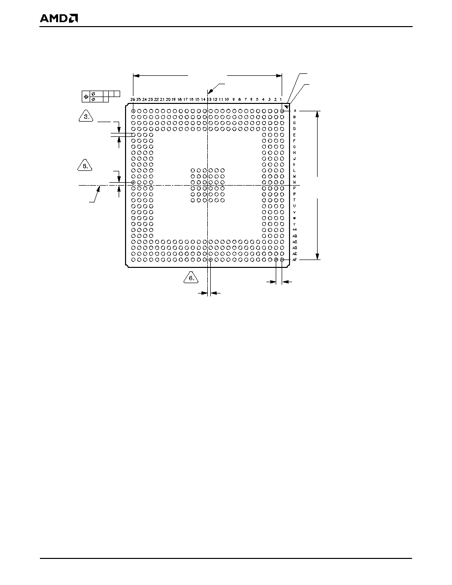
B-2
…lanTMSC520 Microcontroller Data Sheet
P R E L I M I N A R Y
Bottom View
BOTTOM VIEW
ALL ROWS AND COLUMNS
0.635
BSC
1.27 BSC
31.75
BSC
A1 CORNER
A1 CORNER I.D.
16-038-BGA388-2
ET118
10.26.98 lv
0.60
0.90
.30
.10
C A B
C
388X
(DATUM B)
0.635
BSC
31.75 BSC
(DATUM A)
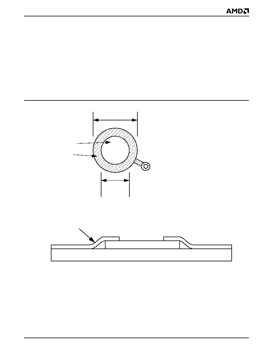
…lanTMSC520 Microcontroller Data Sheet
B-3
P R E L I M I N A R Y
Circuit Board Layout Considerations
There are two basic ways to set up a BGA ball pad, sol-
der-mask defined and solder-pad defined.
s
Solder-mask defined is when the solder mask
opening is smaller than the copper pad, so the
solder surface is defined by the solder mask rather
than the copper pad.
s
Solder-pad defined is when the copper pad is
smaller than the solder mask, so the solder surface
is defined by the copper pad.
A problem can occur when you mix these two methods.
For example, if the chip is solder-pad defined and the
board is pad-defined, then a problem can occur where
there is more surface area on the board making contact
than on the part itself. When the part heats and cools,
a different amount of stress is placed on the chip than
on the board (because there is more surface area sol-
dered on the board), and the chip can warp. The pad
definition on the board should match the chip.
The …lanSC520 microcontroller is solder-mask de-
fined, so the circuit board design should be solder-
mask defined with a solder-mask opening of 0.60 mm
over a 0.80-mm pad as shown in Figure 41.
Figure 41.
BGA Ball Pad Layout
Copper Pad
0.80 mm
Solder
0.60 mm
Mask
Opening
Exposed Copper
Solder Mask
Covered Copper
Top View of BGA Pad
Printed Circuit Board
Copper Pad
Solder Mask
Side View of BGA Pad

B-4
…lanTMSC520 Microcontroller Data Sheet
P R E L I M I N A R Y
…lanTMSC520 Microcontroller Data Sheet
C-1
P R E L I M I N A R Y
Table 21.
Related AMD Products--E86TM Family Devices
Device
1
Notes:
1. 186 = 16-bit microcontroller and 80C186-compatible (except where noted otherwise); 188 = 16-bit microcontroller with 8-bit
external data bus and 80C188-compatible (except where noted otherwise); LV = low voltage
Description
80C186/80C188
16-bit microcontroller
80L186/80L188
Low-voltage, 16-bit microcontroller
Am186TMEM/Am188TMEM
High-performance, 16-bit embedded microcontroller
Am186EMLV/Am188EMLV
High-performance, 16-bit embedded microcontroller
Am186ES/Am188ES
High-performance, 16-bit embedded microcontroller
Am186ESLV/Am188ESLV
High-performance, 16-bit embedded microcontroller
Am186ED
High-performance, 80C186- and 80C188-compatible, 16-bit embedded microcontroller with 8- or
16-bit external data bus
Am186EDLV
High-performance, 80C186- and 80C188-compatible, low-voltage, 16-bit embedded
microcontroller with 8- or 16-bit external data bus
Am186ER/Am188ER
High-performance, low-voltage, 16-bit embedded microcontroller with 32 Kbyte of internal RAM
Am186CC
High-performance, 16-bit embedded communications controller
Am186CH
High-performance, 16-bit embedded HDLC microcontroller
Am186CU
High-performance, 16-bit embedded USB microcontroller
…lanSC300
High-performance, highly integrated, low-voltage, 32-bit embedded microcontroller
…lanSC310
High-performance, single-chip, 32-bit embedded PC/AT-compatible microcontroller
…lanSC400
High-performance, single-chip, low-power, PC/AT-compatible microcontroller
…lanSC410
High-performance, single-chip, PC/AT-compatible microcontroller
…lanSC520
High-performance, single-chip, 32-bit embedded microcontroller
Am386ÆDX
High-performance, 32-bit embedded microprocessor with 32-bit external data bus
Am386ÆSX
High-performance, 32-bit embedded microprocessor with 16-bit external data bus
Am486ÆDX
High-performance, 32-bit embedded microprocessor with 32-bit external data bus
Am
x
586Æ
High-performance, 32-bit embedded microprocessor with 32-bit external data bus
AMD-K6TME
High-performance, 32-bit embedded microprocessor with 64-bit external data bus
AMD-K6TM-2E
High-performance, 32-bit embedded microprocessor with 64-bit external data bus
and 3DNow!TM technology
Am386ÆSX/DX
Microprocessors
Am486ÆDX
Microprocessor
E86TM Family of Embedded Microprocessors and Microcontrollers
Am186ES and
Am188TMEM
Am188EMLV
Microcontrollers
Am188ER
-- Microprocessors
-- 16- and 32-bit microcontrollers
-- 16-bit microcontrollers
AMD-K6TME
Microprocessor
AMD-K6TM-2E
Microprocessor
Am5
x
86
Microprocessor
Am186CC
Communications
Controller
Am186TMCU USB
Microcontroller
Am186CH HDLC
Microcontroller
80C186 and 80C188
Microcontrollers
Am188ES
Microcontrollers
Am186EM and
Microcontrollers
80L186 and 80L188
Microcontrollers
Am186EMLV &
Microcontrollers
Am186ESLV &
Am188ESLV
Am186ER and
Microcontrollers
Am186ED
Am186EDLV
Microcontroller
Microcontroller
APPENDIX C
CUSTOMER SUPPORT
…lanTMSC310
Microcontroller
…lanSC300
Microcontroller
…lanSC410
Microcontroller
…lanSC400
Microcontroller
…lanSC520
Microcontroller

C-2
…lanTMSC520 Microcontroller Data Sheet
P R E L I M I N A R Y
Related Documents
The following documents contain additional information
that will be useful in designing an embedded applica-
tion based on the …lanSC520 microcontroller.
s
…lanTMSC520 Microcontroller Register Set Manual
,
order #22005, fully describes all the registers re-
quired to program the microcontroller.
s
…lanTMSC520 Microcontroller User's Manual
, order
#22004, provides a functional description of the mi-
crocontroller for both hardware and software de-
signers.
s
The Am486Æ
Microprocessor Software User's Man-
ual,
order #18497, includes the complete instruction
set for the integrated Am5
x
86 CPU.
Other information of interest:
s
Am5
x
86
Æ
Microprocessor Family Data Sheet
, order
#19751
s
Am486
Æ
DX/DX2 Microprocessor Hardware Refer-
ence Manual
, order #17965
s
E86 Family Products and Development Tools CD
,
order #21058, provides a single-source multimedia
tool for customer evaluation of AMD products, as
well as FusionE86 partner tools and technologies
that support the E86TM family. Technical documen-
tation is included on the CD in PDF format.
To order literature, contact the nearest AMD sales of-
fice or call the literature center at one of the numbers
listed on the back cover of this manual. In addition, all
these documents are available in PDF form on the
AMD web site. To access the AMD home page, go to
www.amd.com. Then follow the Embedded Processor
link for information about E86 microcontrollers.
Additional Information
The following non-AMD documents and sources pro-
vide additional information that may be of interest to
…lanSC520 microcontroller users:
s
PCI Local Bus Specification
, December 18, 1998,
PCI Special Interest Group, 800-433-5177 (US),
503-693-6232 (International), www.pcisig.com.
s
IEEE Std 1149.1-1990 Standard Test Access Port
a n d B o u n d a r y - S c a n A r c h i t e c t u r e ,
( o r d e r
#SH16626-NYF), Institute of Electrical and Elec-
t r o n i c E n g i n e e r s , I n c . , 8 0 0 - 6 7 8 - 4 3 3 3 ,
www.ieee.org.
s
PCI System Architecture
, Mindshare, Inc., Reading,
MA: Addison-Wesley, 1995, ISBN 0-201-40993-3.
s
ISA System Architecture
, Mindshare, Inc., Reading,
MA: Addison-Wesley, 1995, ISBN 0-201-40996-8.
s
80486 System Architecture, Mindshare, Inc., Read-
ing, MA: Addison-Wesley, 1995, ISBN 0-201-
40994-1
s
The Indispensable PC Hardware Book
, Hans-Peter
Messmer, Wokingham, England: Addison-Wesley,
1995, ISBN 0-201-87697-3.
Customer Development Platform
The …lanSC520 microcontroller customer develop-
ment platform (CDP) is provided as a test and develop-
ment platform to illustrate the capabilities of the
…lanSC520 microcontroller using the PCI bus and an
on-board 10/100 Mbit/s Ethernet connection. In addi-
tion, the CDP serves as a platform for embedded prod-
uct development using the …lanSC520 microcontroller,
Am79C972 Ethernet controller, and the PCI bus.
The …lanSC520 microcontroller CDP enables develop-
ers to benchmark their embedded, network-ready ap-
plica tio ns, u nde rst and th e fu nction ality o f th e
microcontroller, and to know how to wire an …lanSC520
microcontroller system using off-the-shelf components.
The CDP board also demonstrates how the embedded
PCI bus controller works well with other PCI-ready pe-
ripherals.
Third-Party Development Support Products
The FusionE86 Program of Partnerships for Applica-
tion Solutions provides the customer with an array of
products designed to meet critical time-to-market
needs. Products and solutions available from the AMD
FusionE86 partners include protocol stacks, emulators,
hardware and software debuggers, board-level prod-
ucts, and software development tools, among others.
In addition, mature development tools and applications
for the x86 platform are widely available in the general
marketplace.

…lanTMSC520 Microcontroller Data Sheet
C-3
P R E L I M I N A R Y
Customer Service
The AMD customer service network includes U.S. of-
fices, international offices, and a customer training cen-
ter. Expert technical assistance is available from the
AMD worldwide staff of field application engineers and
factory support staff to answer E86 and Comm86 fam-
ily hardware and software development questions.
Hotline and World Wide Web Support
For answers to technical questions, AMD provides
e-mail support as well as a toll-free number for direct
access to our corporate applications hotline.
The AMD World Wide Web home page provides the lat-
est product information, including technical information
and data on upcoming product releases. In addition,
EPD CodeKit software on the Web site provides tested
source code example applications.
Additional contact information is listed on the back of
this datasheet. For technical support questions on all
E86 and Comm86 products, send e-mail to
epd.support@amd.com.
World Wide Web Home Page
To access the AMD home page go to: www.amd.com.
Then follow the Embedded Processors link for infor-
mation about E86 family and Comm86TM products.
Questions, requests, and input concerning AMD's
WWW pages can be sent via e-mail to
web.feedback@amd.com.
Documentation and Literature
Free information such as data books, user's manuals,
data sheets, application notes, the
E86TM Family Prod-
ucts and Development Tools CD
, order #21058, and
other literature is available with a simple phone call. In-
ternationally, contact your local AMD sales office for
product literature, or go to www.amd.com/support/lit-
erature.html. Additional contact information is listed
on the back of this data sheet.
Corporate Applications Hotline
(800) 222-9323
Toll-free for U.S. and Canada
44-(0) 1276-803-299
U.K. and Europe hotline
Literature Ordering
(800) 222-9323
Toll-free for U.S. and Canada

C-4
…lanTMSC520 Microcontroller Data Sheet
P R E L I M I N A R Y

…lanTMSC520 Microcontroller Data Sheet
Index-1
P R E L I M I N A R Y
INDEX
A
a20 gate, 32
address mapping, 31
AMDebug technology
description, 30
parallel, 30
pin summary, A-13
serial, 30
signal descriptions, 23
applications
description, 33
digital set top box, 36
Smart Residential Gateway, 34
thin client, 35
architecture
overview, 28
x86 instruction set, 30
B
block diagram, 29
bootstraps
See
configuration.
C
capacitance
crystal, 51
derating curves, 51
non-PCI interface, 51
PCI interface, 51
chip select
GP bus signal description, 24
circuit board layout, B-3
clock
32.768-kHz crystal selection, 41
33.333-MHz crystal speed, 43
33-MHz crystal selection, 42
backup battery, 46
circuit diagrams, 46
block diagram of clock source, 39
bypassing internal oscillators, 44
circuit with backup battery, 47
circuit without backup battery, 47
control, 38
crystal selection, 41
crystal speeds, 38
generation and control, 38
internal, 39
multiplexed signal trade-offs, A-3
not using backup battery, 46
overview, 31
pin loading, 40
pin summary, A-13
real-time clock (RTC) voltage monitor, 45
RTC voltage monitor block diagram, 45
RTC voltage monitor specifications, 46
SDRAM clock timing, 68
signal descriptions, 22
specifications, 40
system clock block diagram, 38
configuration
multiplexed signal trade-offs, A-3
signal descriptions, 26
CPU
x86 instruction set, 30
crystal
32.768-kHz crystal circuit, 41
32.768-kHz crystal selection, 41
33.333-MHz crystal speed, 43
33-MHz crystal selection, 42
3rd overtone crystal circuit implementation, 42
capacitance, 51
crystal speeds, 38
selecting, 41
customer support
customer development platform, C-2
documentation and literature, C-3
hotline and web, C-3
literature ordering, C-3
ordering the microcontroller, 2
related AMD products/devices, C-1
related documents/information, C-2
third-party development support products, C-2
web home page, C-3
D
DC characteristics, 50
operating ranges, 48
voltage for non-PCI interface pins, 49, 51
debugging
See also
AMDebug technology.
features and system test, 32

P R E L I M I N A R Y
Index-2
…lanTMSC520 Microcontroller Data Sheet
JTAG boundary scan test interface, 32
JTAG signal descriptions, 23
derating curves, 51
DMA
GP bus DMA read cycle, 71
GP bus DMA write cycle, 72
integrated controller, 31
documentation
See
customer support.
DRAM
See
SDRAM.
E
…lanTMSC520 microcontroller
application examples, 33
architectural overview, 28
block diagram, 29
capacitance, 51
circuit board layout, B-3
DC characteristics, 50
distinctive characteristics, 1
documentation, C-2
general description, 1
logic diagram by default pin function, 7
logic diagram by interface, 6
maximum ratings, 48
operating ranges, 48
ordering information, 2
PBGA package, B-1
peripherals (overview), 31
physical dimensions, B-1
pin connection diagram, 8
pin designations, 10
pin tables (Appendix A), A-1
power characteristics, 56
programmable address region (PAR) registers, 31
related AMD E86 family devices, C-1
switching characteristics and waveforms, 58
thermal characteristics, 56
voltage levels, 48≠49
F
Flash
addressing mapping, 31
controller description, 30
multiplexed signal trade-offs, A-2
pin summary, A-8
signal descriptions, 18
write cycles, 65
G
GP bus
chip-select signal descriptions, 24
description, 31
DMA read cycle, 71
DMA write cycle, 72
multiplexed signal trade-offs, A-2
pin summary, A-10
signal descriptions, 19
timing, 69
ground
pin summary, A-14
H
hotline and world wide web support, C-3
I
I/O
programmable I/O (PIO) signal descriptions, 25
interrupts
programmable interrupt controller (PIC), 31
J
JTAG
boundary scan test interface, 32
pin summary, A-13
signal descriptions, 23
timing, 74
L
literature
See
customer support.
logic diagram
by default pin function, 7
by interface, 6
M
maximum ratings, 48
multiplexed functions
signal trade-offs, A-2
N
no connect (NC)
pin summary, A-16

P R E L I M I N A R Y
…lanTMSC520 Microcontroller Data Sheet
Index-3
O
operating ranges, 48
ordering information, 2
P
package
PBGA physical dimensions, B-1
PAR
programmable address region registers, 31
PBGA package
physical dimensions, B-1
thermal characteristics, 56
PCI bus
AC timing, 58
capacitance, 51
description, 30
pin summary, A-8
signal descriptions, 18
switching test waveforms, 58
timing, 65
voltage, 49
peripherals
integrated, description of, 31
physical dimensions, B-1
PIC (programmable interrupt controller), 31
pins
See also
signals.
clock pin loading, 40
pin and signal tables, 10
pin connection diagram, 8
pin designations, 10
pin designations by pin name, 13
pin designations sorted by pin number, 11
pin tables (Appendix A), A-1
Multiplexed Signal Trade-Offs table, A-2
Pin List Summary table, A-7
PIOs Sorted by PIO Number table, A-4
PIOs Sorted by Signal Name table, A-5
PIO
See
programmable I/O (PIO).
power
characteristics, 56
pin summary, A-14
power dissipation, 56
signal descriptions, 27
supply current, 56
voltage levels, 48
power-on reset
timing, 59
programmable I/O (PIO)
multiplexed signal trade-offs, A-3
signal descriptions, 25
sorted by pin number, A-4
sorted by signal name, A-5
R
real-time clock (RTC)
backup battery, 46
circuit with backup battery, 47
circuit without backup battery, 47
not using backup battery, 46
voltage monitor, 45
voltage monitor block diagram, 45
voltage monitor specifications, 46
reset
pin summary, A-13
power-on reset timing, 59
signal descriptions, 22
soft CPU reset, 32
timing with power applied, 61
ROM
address mapping, 31
controller description, 30
multiplexed signal trade-offs, A-2
pin summary, A-8
signal descriptions, 18
timing, 63
RTC
See
real-time clock (RTC).
S
SDRAM
address mapping, 31
clock timing, 68
controller description, 30
error correction code (ECC), 30
pin summary, A-7
signal descriptions, 17
timing, 66
serial ports
multiplexed signal trade-offs, A-2
pin summary, A-12
signal descriptions, 21
signals
See also
pins.
multiplexed signal trade-offs table, A-2
signal description table, 17
signal descriptions, 16
software timer, 32
SSI
See
synchronous serial interface (SSI).
switching characteristics and waveforms
GP bus, 69
JTAG, 74
non-PCI bus interface pins, 58

P R E L I M I N A R Y
Index-4
…lanTMSC520 Microcontroller Data Sheet
over commercial/industrial operating ranges, 59
PCI bus, 65
PCI bus interface pins, 58
power-on reset, 59
reset with power applied, 61
ROM, 63
SDRAM, 66
SSI, 73
synchronous serial interface (SSI)
description, 32
timing, 73
system test
multiplexed signal trade-offs, A-3
pin summary, A-13
signal descriptions, 23
T
technical support
See
customer support.
testing
JTAG boundary scan test interface, 32
system test and debug features, 32
system test multiplexed signal trade-offs, A-3
system test pin summary, A-13
system test signal descriptions, 23
thermal characteristics, 56
equations, 57
timers
description, 32
multiplexed signal trade-offs, A-3
pin summary, A-14
signal descriptions, 25
timing
See
switching characteristics and waveforms.
U
UARTs
description, 32
V
voltage
for non-PCI interface pins, 49
for PCI interface pins, 49
maximum ratings, 48
operating ranges, 48
W
watchdog timer, 32
www
home page, C-3
support, C-3

…lanTMSC520 Microcontroller Data Sheet
P R E L I M I N A R Y
Trademarks
AMD, the AMD logo, and combinations thereof, AMD Athlon, …lan, AMDebug, PCnet, E86, Am186, Am188 and Comm86 are trademarks;
Am5
x
86, Am386, Am486 and AMD-K6 are registered trademarks and FusionE86 is a servicemark of Advanced Micro Devices, Inc.
Microsoft and Windows are registered trademarks of Microsoft Corporation.
Other product names used in this publication are for identification purposes only and may be trademarks of their respective companies.
Disclaimer
The contents of this document are provided in connection with Advanced Micro Devices, Inc. ("AMD") products. AMD makes no representations
or warranties with respect to the accuracy or completeness of the contents of this publication and reserves the right to make changes to speci-
fications and product descriptions at any time without notice. No license, whether express, implied, arising by estoppel or otherwise, to any intel-
lectual property rights is granted by this publication. Except as set forth in AMD's Standard Terms and Conditions of Sale, AMD assumes no
liability whatsoever, and disclaims any express or implied warranty, relating to its products including, but not limited to, the implied warranty of
merchantability, fitness for a particular purpose, or infringement of any intellectual property right.
AMD's products are not designed, intended, authorized or warranted for use as components in systems intended for surgical implant into the
body, or in other applications intended to support or sustain life, or in any other application in which the failure of AMD's product could create a
situation where personal injury, death, or severe property or environmental damage may occur. AMD reserves the right to discontinue or make
changes to its products at any time without notice.
©2001 Advanced Micro Devices, Inc.
All rights reserved.