
Publication Number S29GLxxxM Revision B Amendment 1 Issue Date August 4, 2004
DATASHEET
S29GLxxxM MirrorBit
TM
Flash Family
S29GL256M, S29GL128M, S29GL064M, S29GL032M
256 Megabit, 128 Megabit, 64 Megabit, and 32Megabit,
3.0 Volt-only Page Mode Flash Memory featuring
0.23 um MirrorBit process technology
Datasheet
Distinctive Characteristics
Architectural Advantages
Single power supply operation
-- 3 volt read, erase, and program operations
Manufactured on 0.23 um MirrorBit process
technology
SecSiTM (Secured Silicon) Sector region
-- 128-word/256-byte sector for permanent, secure
identification through an 8-word/16-byte random
Electronic Serial Number, accessible through a
command sequence
-- May be programmed and locked at the factory or by
the customer
Flexible sector architecture
-- 256Mb: 512 32 Kword (64 Kbyte) sectors
-- 128Mb: 256 32 Kword (64 Kbyte) sectors
-- 64Mb (uniform sector models): 128 32 Kword (64
Kbyte) sectors or 128 32 Kword sectors
-- 64Mb (boot sector models): 127 32 Kword (64 Kbyte)
sectors + 8 4Kword (8Kbyte) boot sectors
-- 32Mb (uniform sector models): 64 32Kword (64
Kbyte) sectors of 64 32Kword sectors
-- 32Mb (boot sector models): 63 32Kword (64 Kbyte)
sectors + 8 4Kword (8Kbyte) boot sectors
Compatibility with JEDEC standards
-- Provides pinout and software compatibility for single-
power supply flash, and superior inadvertent write
protection
100,000 erase cycles typical per sector
20-year data retention typical
Performance Characteristics
High performance
-- 90 ns access time (128Mb, 64Mb, 32Mb),
100 ns access time (256Mb)
-- 4-word/8-byte page read buffer
-- 25 ns page read times (128Mb, 64Mb, 32Mb)
-- 30 ns page read times (256Mb)
-- 16-word/32-byte write buffer
-- 16-word/32-byte write buffer reduces overall
programming time for multiple-word updates
Low power consumption (typical values at 3.0 V, 5
MHz)
-- 18 mA typical active read current (64 Mb, 32 Mb)
-- 25 mA typical active read current (256 Mb, 128 Mb)
-- 50 mA typical erase/program current
-- 1 µA typical standby mode current
Package options
-- 40-pin TSOP
-- 48-pin TSOP
-- 56-pin TSOP
-- 64-ball Fortified BGA
-- 48-ball fine-pitch BGA
-- 63-ball fine-pitch BGA
Software & Hardware Features
Software features
-- Program Suspend & Resume: read other sectors
before programming operation is completed
-- Erase Suspend & Resume: read/program other
sectors before an erase operation is completed
-- Data# polling & toggle bits provide status
-- CFI (Common Flash Interface) compliant: allows host
system to identify and accommodate multiple flash
devices
-- Unlock Bypass Program command reduces overall
multiple-word programming time
Hardware features
-- Sector Group Protection: hardware-level method of
preventing write operations within a sector group
-- Temporary Sector Unprotect: V
ID
-level method of
charging code in locked sectors
-- WP#/ACC input accelerates programming time
(when high voltage is applied) for greater throughput
during system production. Protects first or last sector
regardless of sector protection settings on uniform
sector models
-- Hardware reset input (RESET#) resets device
-- Ready/Busy# output (RY/BY#) detects program or
erase cycle completion

2
S29GLxxxM MirrorBit
TM
Flash Family
S29GLxxxM_00_B1_E August 4, 2004
D a t a s h e e t
General Description
The S29GL256/128/064/032M family of devices are 3.0 V single power Flash memory manufactured using 0.23
um MirrorBit technology. The S29GL256M is a 256 Mbit, organized as 16,777,216 words or 33,554,432 bytes. The
S29GL128M is a 128 Mbit, organized as 8,388,608 words or 16,777,216 bytes. The S29GL064M is a 64 Mbit, or-
ganized as 4,194,304 words or 8,388,608 bytes. The S29GL032M is a 32 Mbit, organized as 2,097,152 words or
4,194,304 bytes. Depending on the model number, the devices have an 8-bit wide data bus only, 16-bit wide data
bus only, or a 16-bit wide data bus that can also function as an 8-bit wide data bus by using the BYTE# input. The
devices can be programmed either in the host system or in standard EPROM programmers.
Access times as fast as 90 ns (S29GL128M, S29GL064M, S29GL032M) or 100 ns (S29GL256M) are available. Note
that each access time has a specific operating voltage range (V
CC
) as specified in the
Product Selector Guide
and
the
Ordering Information
sections. Package offerings include 40-pin TSOP, 48-pin TSOP, 56-pin TSOP, 48-ball fine-
pitch BGA, 63-ball fine-pitch BGA and 64-ball Fortified BGA, depending on model number. Each device has sepa-
rate chip enable (CE#), write enable (WE#) and output enable (OE#) controls.
Each device requires only a single 3.0 volt power supply for both read and write functions. In addition to a V
CC
input, a high-voltage accelerated program (ACC) feature provides shorter programming times through in-
creased current on the WP#/ACC input. This feature is intended to facilitate factory throughput during system
production, but may also be used in the field if desired.
The device is entirely command set compatible with the JEDEC single-power-supply Flash standard. Com-
mands are written to the device using standard microprocessor write timing. Write cycles also internally latch
addresses and data needed for the programming and erase operations.
The sector erase architecture allows memory sectors to be erased and reprogrammed without affecting the
data contents of other sectors. The device is fully erased when shipped from the factory.
Device programming and erasure are initiated through command sequences. Once a program or erase operation
has begun, the host system need only poll the DQ7 (Data# Polling) or DQ6 (toggle) status bits or monitor the
Ready/Busy# (RY/BY#) output to determine whether the operation is complete. To facilitate programming, an
Unlock Bypass mode reduces command sequence overhead by requiring only two write cycles to program data
instead of four.
Hardware data protection measures include a low V
CC
detector that automatically inhibits write operations dur-
ing power transitions. The hardware sector protection feature disables both program and erase operations in any
combination of sectors of memory. This can be achieved in-system or via programming equipment.
The Erase Suspend/Erase Resume feature allows the host system to pause an erase operation in a given sector
to read or program any other sector and then complete the erase operation. The Program Suspend/Program
Resume feature enables the host system to pause a program operation in a given sector to read any other sector
and then complete the program operation.
The hardware RESET# pin terminates any operation in progress and resets the device, after which it is then
ready for a new operation. The RESET# pin may be tied to the system reset circuitry. A system reset would thus
also reset the device, enabling the host system to read boot-up firmware from the Flash memory device.
The device reduces power consumption in the standby mode when it detects specific voltage levels on CE# and
RESET#, or when addresses have been stable for a specified period of time.
The Write Protect (WP#) feature protects the first or last sector by asserting a logic low on the WP#/ACC pin
or WP# pin, depending on model number. The protected sector will still be protected even during accelerated
programming.
The SecSiTM (Secured Silicon) Sector provides a 128-word/256-byte area for code or data that can be perma-
nently protected. Once this sector is protected, no further changes within the sector can occur.
Spansion MirrorBit flash technology combines years of Flash memory manufacturing experience to produce the
highest levels of quality, reliability and cost effectiveness. The device electrically erases all bits within a sector
simultaneously via hot-hole assisted erase. The data is programmed using hot electron injection.

August 4, 2004 S29GLxxxM_00_B1_E
S29GLxxxM MirrorBit
TM
Flash Family
3
Table of Contents
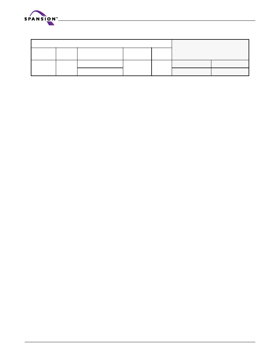
Product Selector Guide . . . . . . . . . . . . . . . . . . . . . .5
S29GL256M .............................................................................................................5
S29GL128M ..............................................................................................................5
S29GL064M .............................................................................................................5
S29GL032M .............................................................................................................5
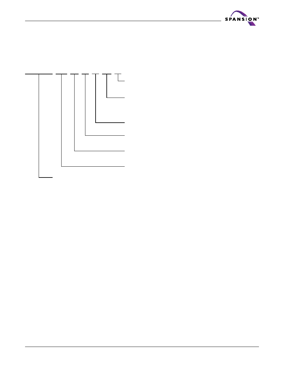
Block Diagram . . . . . . . . . . . . . . . . . . . . . . . . . . . . 6
Connection Diagrams . . . . . . . . . . . . . . . . . . . . . . .7
For S29GL064M (model R0) only. ...................................................................9
For S29GL064M (model R0) only. ..................................................................13
Logic Symbol-S29GL032M (Model R0) ..........................................................17
Logic Symbol-S29GL032M (Models R1, R2) ..................................................17
Logic Symbol-S29GL032M (Models R3, R4) .................................................17
Logic Symbol-S29GL064M (Models R0) ....................................................... 18
Logic Symbol-S29GL064M (Models R1, R2) ................................................ 18
Logic Symbol-S29GL064M (Models R3, R4) ............................................... 18
Logic Symbol-S29GL064M (Model R5) ......................................................... 19
Logic Symbol-S29GL064M (Model R6, R7) ................................................. 19
Logic Symbol-S29GL128M ................................................................................. 19
Logic Symbol-S29GL256M ............................................................................... 20
Ordering Information-S29GL032M . . . . . . . . . . . . 21
S29GL032M Standard Products ...................................................................... 21
Table 1. S29GL032M Ordering Options ................................. 22
Ordering Information-S29GL064M . . . . . . . . . . . . 23
S29GL064M Standard Products ......................................................................23
Table 2. S29GL064M Ordering Options ................................. 24
Ordering Information-S29GL128M . . . . . . . . . . . .25
S29GL128M Standard Products .......................................................................25
Table 3. S29GL128M Ordering Options ................................. 26
Ordering Information-S29GL256M . . . . . . . . . . . .27
S29GL256M Standard Products ......................................................................27
Table 4. S29GL256M Ordering Options ................................. 28
Device Bus Operations . . . . . . . . . . . . . . . . . . . . . .29
Table 5. Device Bus Operations ........................................... 29
Word/Byte Configuration ................................................................................30
Requirements for Reading Array Data ........................................................ 30
Page Mode Read ............................................................................................. 30
Writing Commands/Command Sequences ................................................ 30
Write Buffer .................................................................................................... 30
Accelerated Program Operation ................................................................31
Autoselect Functions ......................................................................................31
Standby Mode ........................................................................................................31
Automatic Sleep Mode .......................................................................................31
RESET#: Hardware Reset Pin ..........................................................................31
Output Disable Mode ........................................................................................32
Table 6. S29GL032M (Model R0) Sector Address Table ........... 32
Table 7. S29GL032M (Models R1, R2) Sector Address Table .... 34
Table 8. S29GL032M (Model R3) Top Boot Sector Architecture 36
Table 9. S29GL032M (Model R4) Bottom Boot Sector
Architecture ...................................................................... 38
Table 10. S29GL064M (Model R0) Sector Address Table ......... 40
Table 11. S29GL064M (Model R1, R2) Sector Address Table .... 44
Table 12. S29GL064M (Model R3) Top Boot Sector Architecture 48
Table 13. S29GL064M (Model R4) Bottom Boot Sector
Architecture ...................................................................... 52
Table 14. S29GL064M (Model R5) Sector Address Table ......... 56
Table 15. S29GL064M (Model R6, R7) Sector Address Table .... 59
Table 16. S29GL128M Sector Address Table ......................... 62
Table 17. S29GL256M Sector Address Table ......................... 68
Autoselect Mode .................................................................................................79
Table 18. Autoselect Codes, (High Voltage Method) ...............80
Sector Group Protection and Unprotection .............................................. 81
Table 19. S29GL032M (Model R0) Sector Group Protection/
Unprotection Address Table ................................................81
Table 20. S29GL032M (Model R1) Top Boot Sector Protection ..82
Table 22. S29GL032M (Models R3, R4) Sector Group
Protection/Unprotection Address Table .................................83
Table 21. S29GL032M (Model R2) Bottom Boot Sector
Protection .........................................................................83
Table 23. S29GL065M (Model 00) Sector Group Protection/
Unprotection Address Table ................................................84
Table 24. S29GL064M (Model R1) Top Boot Sector Protection ..85
Table 25. S29GL064M (Model R2) Bottom Boot Sector
Protection .........................................................................86
Table 26. S29GL064M (Models R3, R4) Sector Group
Protection/Unprotection Address Table .................................87
Table 27. S29GL064M (Model R5) Sector Group Protection/
Unprotection Address Table ................................................88
Table 28. S29GL064M (Models R6, R7) Sector Group
Protection/Unprotection Address Table .................................89
Table 29. S29GL128M Sector Group Protection/Unprotection
Address Table ....................................................................90
Table 30. S29GL256M Sector Group Protection/Unprotection
Address Table ....................................................................92
Temporary Sector Group Unprotect .......................................................... 95
Figure 1. Temporary Sector Group Unprotect Operation .......... 95
Figure 2. In-System Sector Group Protect/Unprotect
Algorithms ........................................................................ 96
SecSi (Secured Silicon) Sector Flash Memory Region ............................. 97
Write Protect (WP#) .......................................................................................98
Hardware Data Protection .............................................................................98
Low VCC Write Inhibit ...............................................................................98
Write Pulse "Glitch" Protection ...............................................................98
Logical Inhibit ...................................................................................................98
Power-Up Write Inhibit ...............................................................................98
Common Flash Memory Interface (CFI) . . . . . . . 99
Table 32. System Interface String...................................... 100
Command Definitions . . . . . . . . . . . . . . . . . . . . . .103
Reading Array Data ..........................................................................................103
Reset Command ................................................................................................103
Autoselect Command Sequence ..................................................................104
Enter SecSi Sector/Exit SecSi Sector Command Sequence ..................104
Word Program Command Sequence .....................................................104
Unlock Bypass Command Sequence .......................................................105
Write Buffer Programming ........................................................................105
Accelerated Program ...................................................................................106
Figure 3. Write Buffer Programming Operation..................... 107
Figure 4. Program Operation ............................................. 108
Program Suspend/Program Resume Command Sequence .................. 108
Figure 5. Program Suspend/Program Resume ...................... 109
Chip Erase Command Sequence ..................................................................109
Sector Erase Command Sequence ................................................................110
Figure 6. Erase Operation ................................................. 111
Erase Suspend/Erase Resume Commands ...................................................111
Command Definitions ........................................................................................113
Table 35. Command Definitions (x16 Mode, BYTE# = V
IH
) .... 113
Table 36. Command Definitions (x8 Mode, BYTE# = V
IL
) ....... 114
Write Operation Status ................................................................................... 115
DQ7: Data# Polling ...........................................................................................115
Figure 7. Data# Polling Algorithm ...................................... 116
RY/BY#: Ready/Busy# .......................................................................................116

4
S29GLxxxM MirrorBit
TM
Flash Family
S29GLxxxM_00_B1_E August 4, 2004
DQ6: Toggle Bit I ............................................................................................... 117
Figure 8. Toggle Bit Algorithm............................................ 118
DQ2: Toggle Bit II ...............................................................................................119
Reading Toggle Bits DQ6/DQ2 .....................................................................119
DQ5: Exceeded Timing Limits .......................................................................119
DQ3: Sector Erase Timer ................................................................................119
DQ1: Write-to-Buffer Abort .........................................................................120
Table 37. Write Operation Status ........................................120
Figure 9. Maximum Negative Overshoot Waveform............... 121
Figure 10. Maximum Positive
Overshoot Waveform........................................................ 121
Operating Ranges . . . . . . . . . . . . . . . . . . . . . . . . . 121
DC Characteristics . . . . . . . . . . . . . . . . . . . . . . . . 122
Test Conditions . . . . . . . . . . . . . . . . . . . . . . . . . . . 123
Figure 11. Test Setup ....................................................... 123
Table 38. Test Specifications ..............................................123
Key to Switching Waveforms . . . . . . . . . . . . . . 123
Figure 12. Input Waveforms and
Measurement Levels......................................................... 123
AC Characteristics . . . . . . . . . . . . . . . . . . . . . . . . 124
Read-Only Operations-S29GL256M only ..................................................124
Read-Only Operations-S29GL128M only ...................................................124
Read-Only Operations-S29GL064M only .................................................. 125
Read-Only Operations-S29GL032M only .................................................. 125
Figure 13. Read Operation Timings ..................................... 126
Figure 14. Page Read Timings............................................ 126
Hardware Reset (RESET#) ............................................................................. 127
Figure 15. Reset Timings................................................... 127
Erase and Program Operations-S29GL256M only ..................................128
Erase and Program Operations-S29GL128M Only .................................129
Erase and Program Operations-S29GL064M Only ................................ 130
Erase and Program Operations-S29GL032M only ....................................131
Figure 16. Program Operation Timings ................................ 131
Figure 17. Accelerated Program Timing Diagram .................. 132
Figure 18. Chip/Sector Erase Operation Timings ................... 133
Figure 19. Data# Polling Timings (During Embedded
Algorithms) ..................................................................... 133
Figure 20. Toggle Bit Timings (During Embedded Algorithms) 134
Figure 21. DQ2 vs. DQ6.................................................... 134
Temporary Sector Unprotect .......................................................................134
Figure 22. Temporary Sector Group Unprotect Timing Diagram 135
Figure 23. Sector Group Protect and Unprotect Timing Diagram 135
Alternate CE# Controlled Erase and Program Operations-
S29GL256M .........................................................................................................136
Alternate CE# Controlled Erase and Program Operations-
S29GL128M .......................................................................................................... 137
Alternate CE# Controlled Erase and Program Operations-
S29GL064M .........................................................................................................138
Alternate CE# Controlled Erase and Program Operations-
S29GL032M .........................................................................................................139
Figure 24. Alternate CE# Controlled Write (Erase/
Program) Operation Timings.............................................. 140
Erase and Programming Performance . . . . . . . . 141
TSOP Pin and BGA Package Capacitance . . . . .142
Physical Dimensions . . . . . . . . . . . . . . . . . . . . . . .143
TS040--40-Pin Standard Thin Small Outline Package ...........................143
TSR040--40-Pin Standard/Reverse Thin Small Outline Package
(TSOP) ..................................................................................................................144
TS048--48-Pin Standard/Reverse Thin Small Outline Package
(TSOP) ..................................................................................................................145
TSR048--48-Pin Standard/Reverse Thin Small Outline Package
(TSOP) ..................................................................................................................146
TS056/TSR056--56-Pin Standard/Reverse Thin Small Outline
Package (TSOP) .................................................................................................147
LAA064--64-Ball Fortified Ball Grid Array (FBGA) ..............................148
LAC064--64-Pin 18 x 12 mm package .........................................................149
FBA048--48-Pin 6.15 x 8.15 mm package ...................................................150
FBC048--48-Pin 8 x 9 mm package ............................................................151
FBE063--63-Pin 12 x 11 mm package ............................................................152
FPT-48P-M19 ....................................................................................................... 153
FPT-56P-M01 ....................................................................................................... 153
BGA-48P-M20 ....................................................................................................154
Revision Summary . . . . . . . . . . . . . . . . . . . . . . . . .155
August 4, 2004 S29GLxxxM_00_B1_E
S29GLxxxM MirrorBit
TM
Flash Family
5
D a t a s h e e t
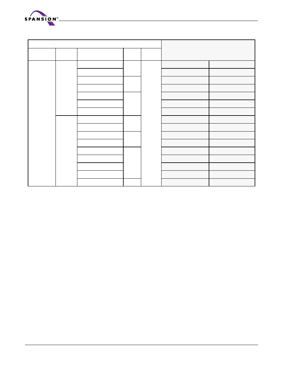
Product Selector Guide
S29GL256M
S29GL128M
S29GL064M
S29GL032M
Part Number
S29GL256M
Speed Option
10
11
Max. Access Time (ns)
100
110
Max. CE# Access Time (ns)
100
110
Max. Page Access Time (ns)
30
30
Max. OE# Access Time (ns)
30
30
Part Number
S29GL128M
Speed Option
90
10
Max. Access Time (ns)
90
100
Max. CE# Access Time (ns)
90
100
Max. Page Access Time (ns)
25
30
Max. OE# Access Time (ns)
25
30
Part Number
S29GL064M
Speed Option
90
10
11
Max. Access Time (ns)
90
100
110
Max. CE# Access Time (ns)
90
100
110
Max. Page Access Time (ns)
25
30
30
Max. OE# Access Time (ns)
25
30
30
Part Number
S29GL032M
Speed Option
90
10
11
Max. Access Time (ns)
90
100
110
Max. CE# Access Time (ns)
90
100
110
Max. Page Access Time (ns)
25
30
30
Max. OE# Access Time (ns)
25
30
30

6
S29GLxxxM MirrorBit
TM
Flash Family
S29GLxxxM_00_B1_E August 4, 2004
D a t a s h e e t
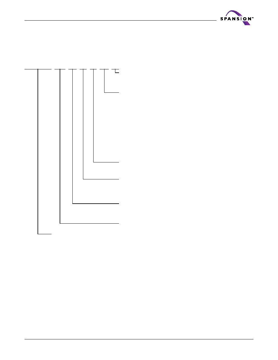
Block Diagram
Input/Output
Buffers
X-Decoder
Y-Decoder
Chip Enable
Output Enable
Logic
Erase Voltage
Generator
PGM Voltage
Generator
Timer
V
CC
Detector
State
Control
Command
Register
V
CC
V
SS
WE#
WP#/ACC
BYTE#
CE#
OE#
STB
STB
DQ15
≠
DQ0 (A-1)
Sector Switches
RY/BY#
RESET#
Data
Latch
Y-Gating
Cell Matrix
Addr
e
ss La
t
c
h
A
Max
**≠A0
August 4, 2004 S29GLxxxM_00_B1_E
S29GLxxxM MirrorBit
TM
Flash Family
7
D a t a s h e e t
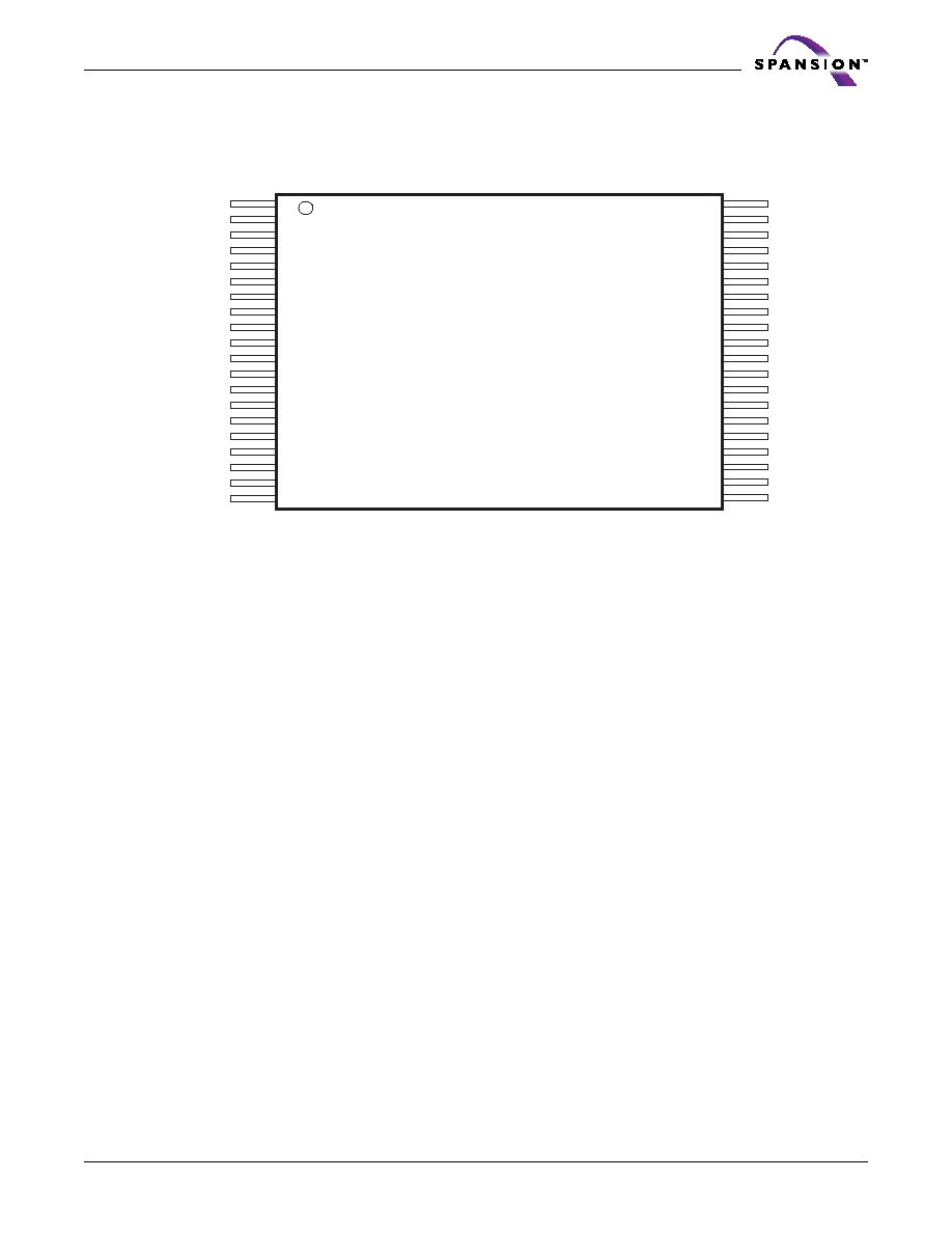
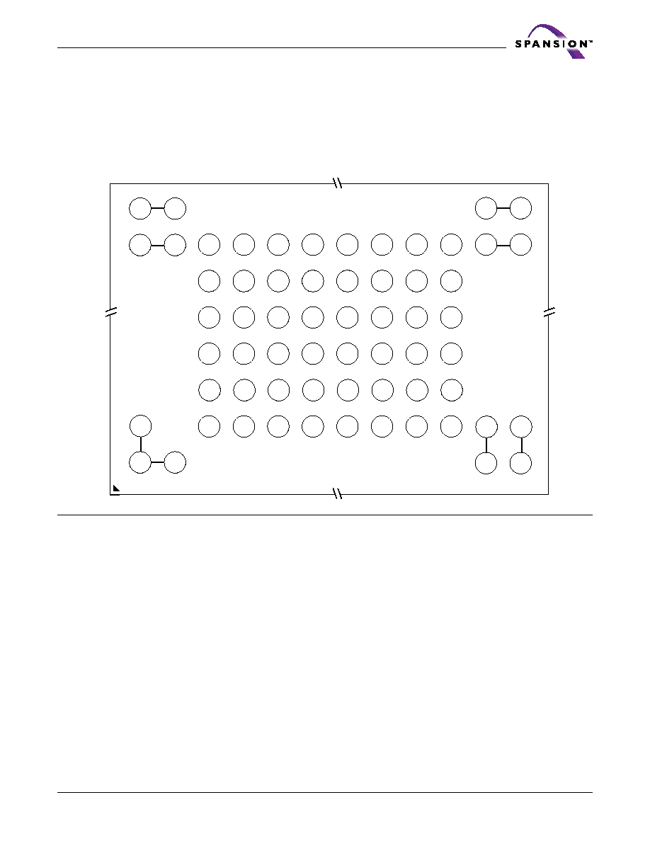
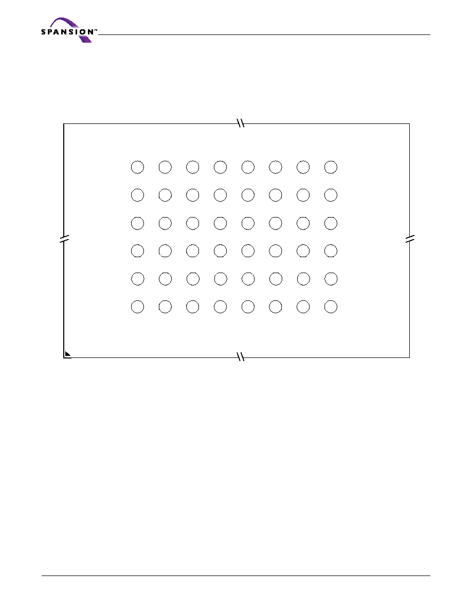
Connection Diagrams
1
16
2
3
4
5
6
7
8
17
18
19
20
9
10
11
12
13
14
15
40
25
39
38
37
36
35
34
33
32
31
30
29
28
27
26
24
23
22
21
A16
A5
A15
A14
A13
A12
A11
A9
A8
WE#
RESET#
ACC
RY/BY#
A18
A7
A6
A4
A3
A2
A1
A17
DQ0
V
SS
A20
A19
A10
DQ7
DQ6
DQ5
OE#
V
SS
CE#
A0
DQ4
V
CC
V
IO
A21
DQ3
DQ2
DQ1
40-Pin Standard TSOP
** A
Max
GL256M = A23
A
Max
GL128M = A22
A
Max
GL064M = A21 (A
Max
GL064M-00 = A22)
A
Max
GL032M = A20 (A
Max
GL032M-00 = A21)

8
S29GLxxxM MirrorBit
TM
Flash Family
S29GLxxxM_00_B1_E August 4, 2004
D a t a s h e e t
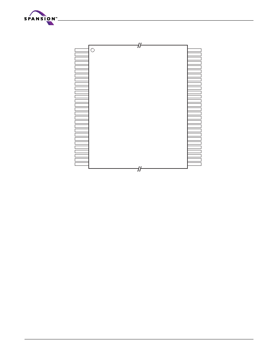
Connection Diagrams
Notes:
1. Pin 13 is NC on S29GL032M.
2. Pin 9 is A21, Pin 13 is ACC, Pin 14 is WP#, Pin 15 is A19, and Pin 47 is V
IO
on S29GL064M (models R6, R7).
1
16
2
3
4
5
6
7
8
17
18
19
20
21
22
23
24
9
10
11
12
13
14
15
48
33
47
46
45
44
43
42
41
40
39
38
37
36
35
34
25
32
31
30
29
28
27
26
A15
A18
A14
A13
A12
A11
A10
A9
A8
A19
2
A20
WE#
RESET#
A21
1,2
WP#/ACC
2
RY/BY#
2
A1
A17
A7
A6
A5
A4
A3
A2
A16
DQ2
BYTE#
2
V
SS
DQ15/A-1
DQ7
DQ14
DQ6
DQ13
DQ9
DQ1
DQ8
DQ0
OE#
V
SS
CE#
A0
DQ5
DQ12
DQ4
V
CC
DQ11
DQ3
DQ10
48-Pin Standard TSOP

August 4, 2004 S29GLxxxM_00_B1_E
S29GLxxxM MirrorBit
TM
Flash Family
9
D a t a s h e e t
Connection Diagrams
For S29GL064M (model R0) only.
1
16
2
3
4
5
6
7
8
17
18
19
20
21
22
23
24
9
10
11
12
13
14
15
40
25
39
38
37
36
35
34
33
32
31
48
47
46
45
44
43
42
41
30
29
28
27
26
A16
A5
A15
NC
A22
A14
A13
A12
A11
A9
A8
WE#
RESET#
ACC
RY/BY#
A18
A7
A6
A4
A3
A2
A1
NC
NC
A17
DQ0
V
SS
NC
NC
NC
NC
A20
A19
A10
DQ7
DQ6
DQ5
OE#
V
SS
CE#
A0
DQ4
V
CC
V
IO
A21
DQ3
DQ2
DQ1
48-Pin Standard TSOP
10
S29GLxxxM MirrorBit
TM
Flash Family
S29GLxxxM_00_B1_E August 4, 2004
D a t a s h e e t
Connection Diagrams
Notes:
1. Pin 1 is NC on S29GL128M, 29GL064M, and S29GL032M.
2. Pin 2 is NC on S29GL064M, and S29GL032M.
3. Pin 15 is NC on S29GL032M.
1
2
3
4
5
6
7
8
9
10
11
12
13
14
15
16
17
18
19
20
21
22
A231
A222
A15
A14
A13
A12
A11
A10
A9
A8
A19
A20
WE#
RESET#
A21
3
WP#/ACC
RY/BY#
A18
A17
A7
A6
A5
56
55
54
53
52
51
50
49
48
47
46
45
44
43
42
41
40
39
38
37
36
35
NC
NC
A16
BYTE#
V
SS
DQ15/A-1
DQ7
DQ14
DQ6
DQ13
DQ5
DQ12
DQ4
V
CC
DQ11
DQ3
DQ10
DQ2
DQ9
DQ1
DQ8
DQ0
23
24
25
26
27
28
A4
A3
A2
A1
NC
NC
34
33
32
31
30
29
OE#
V
SS
CE#
A0
NC
V
IO
56-Pin Standard TSOP
August 4, 2004 S29GLxxxM_00_B1_E
S29GLxxxM MirrorBit
TM
Flash Family
11
D a t a s h e e t
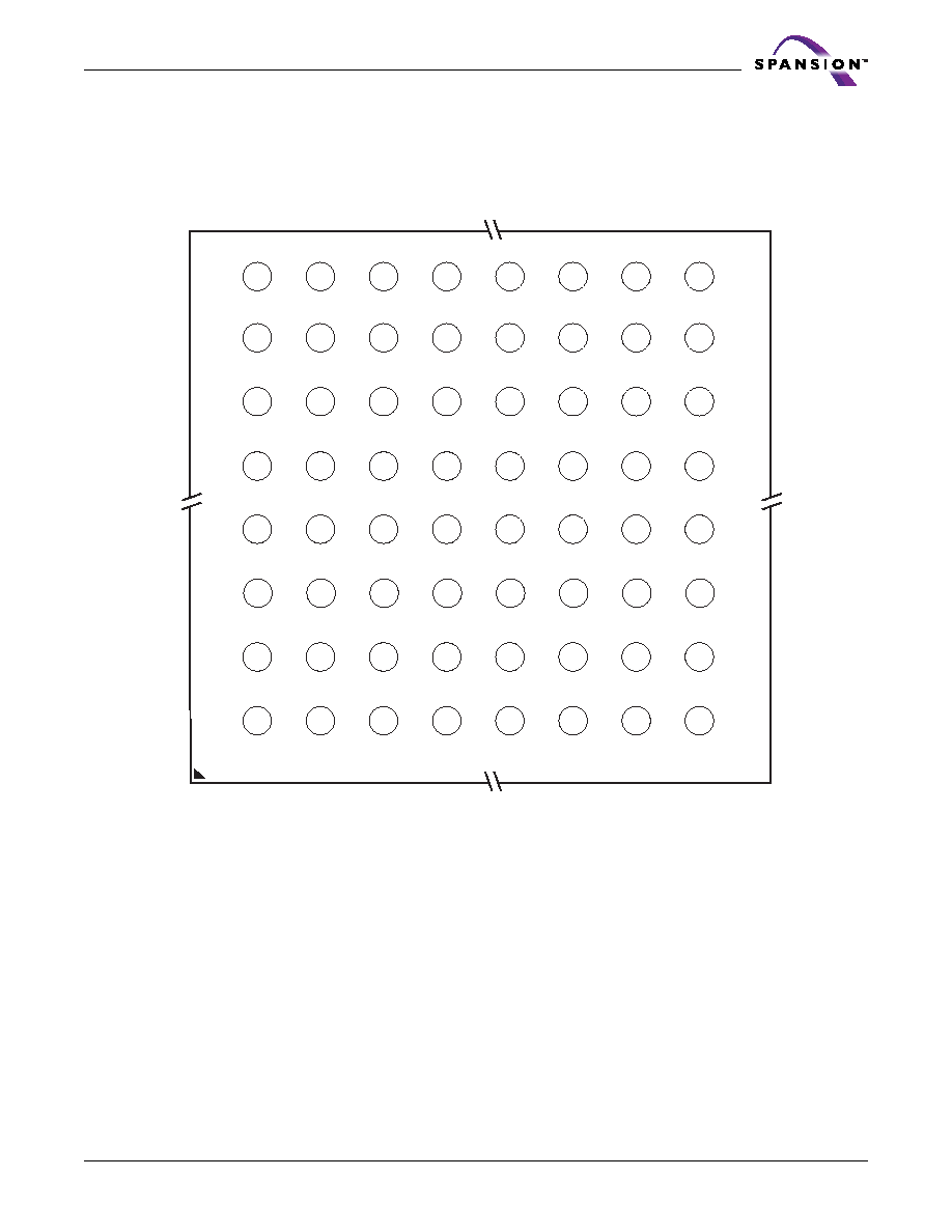
Connection Diagrams
Notes:
1. Ball C5 is NC on S29GL032M.
2. Ball B8 is NC on S29GL064M and S29GL032M.
3. Ball C8 is NC on S29GL128M, S29GL064M and S29GL032M.
4. Ball D8 and Ball F1 are NC on S29GL064M (models R3, R4).
5. Ball F7 is NC on S29GL064M (model R5).
Special Package Handling Instructions
Special handling is required for Flash Memory products in moulded packages (TSOP and BGA). The package and/
or data integrity may be compromised if the package body is exposed to temperatures above 150∞C for prolonged
periods of time.
A2
C2
D2
E2
F2
G2
H2
A3
C3
D3
E3
F3
G3
H3
A4
C4
D4
E4
F4
G4
H4
A5
C5
D5
E5
F5
G5
H5
A6
C6
D6
E6
F6
G6
H6
A7
C7
D7
E7
F7
G7
H7
DQ15/A-1
V
SS
BYTE#
5
A16
A15
A14
A12
A13
DQ13
DQ6
DQ14
DQ7
A11
A10
A8
A9
V
CC
DQ4
DQ12
DQ5
A19
A21
1
RESET#
WE#
DQ11
DQ3
DQ10
DQ2
A20
A18
WP#/ACC
RY/BY#
DQ9
DQ1
DQ8
DQ0
A5
A6
A17
A7
OE#
V
SS
CE#
A0
A1
A2
A4
A3
A1
C1
D1
E1
F1
G1
H1
NC
NC
V
IO
4
NC
NC
NC
NC
NC
A8
C8
B2
B3
B4
B5
B6
B7
B1
B8
D8
E8
F8
G8
H8
NC
NC
NC
V
SS
V
IO
4
A23
3
A22
2
NC
64-ball Fortified BGA
Top View, Balls Facing Down

12
S29GLxxxM MirrorBit
TM
Flash Family
S29GLxxxM_00_B1_E August 4, 2004
D a t a s h e e t
Connection Diagrams
Notes:
1. Ball H7 is V
IO
on S29GL064M (model R5).
Special Package Handling Instructions
Special handling is required for Flash Memory products in molded packages (TSOP and BGA). The package and/
or data integrity may be compromised if the package body is exposed to temperatures above 150∞C for prolonged
periods of time.
C2
D2
E2
F2
G2
H2
J2
K2
C3
D3
E3
F3
G3
H3
J3
K3
C4
D4
E4
F4
G4
H4
J4
K4
C5
D5
E5
F5
G5
H5
J5
K5
C6
D6
E6
F6
G6
H6
J6
K6
C7
D7
A7
B7
A8
B8
A1
B1
A2
E7
F7
G7
H7
J7
K7
L7
L8
M7
M8
L1
L2
M1
M2
NC*
NC*
NC*
NC*
NC*
NC*
NC*
NC*
NC*
NC*
NC*
NC*
NC*
NC*
NC*
DQ15/A-1
V
SS
BYTE#
1
A16
A15
A14
A12
A13
DQ13
DQ6
DQ14
DQ7
A11
A10
A8
A9
V
CC
DQ4
DQ12
DQ5
A19
A21
RESET#
WE#
DQ11
DQ3
DQ10
DQ2
A20
A18
WP#/ACC
RY/BY#
DQ9
DQ1
DQ8
DQ0
A5
A6
A17
A7
OE#
V
SS
CE#
A0
A1
A2
A4
A3
* Balls are shorted together via the substrate but not connected to the die.
63-Ball Fine-Pitch BGA
Top View, Balls Facing Down
August 4, 2004 S29GLxxxM_00_B1_E
S29GLxxxM MirrorBit
TM
Flash Family
13
D a t a s h e e t
Connection Diagrams
For S29GL064M (model R0) only.
Special Package Handling Instructions
Special handling is required for Flash Memory products in molded packages (TSOP and BGA). The package and/
or data integrity may be compromised if the package body is exposed to temperatures above 150∞C for prolonged
periods of time.
C2
D2
C3
D3
E2
E3
F2
F3
G2
G3
H2
H3
J2
J3
K2
A3
A4
A2
A1
A0
CE#
OE#
V
SS
A7
A18
A6
A5
DQ0
NC
NC
DQ1
RY/BY#
ACC
NC
NC
DQ2
DQ3
V
IO
A21
WE#
RESET#
A22
NC
DQ5
NC
V
CC
DQ4
A9
A8
A11
A12
A19
A10
DQ6
DQ7
A14
A13
A15
A16
A17
NC
A20
V
SS
C4
D4
E4
A1
B1
A2
NC*
NC*
NC*
F4
G4
H4
J4
K4
C5
D5
E5
F5
G5
H5
J5
K5
C6
D6
E6
F6
G6
H6
J6
K6
C7
D7
E7
NC*
NC*
NC*
NC*
A7
B7
A8
B8
F7
G7
H7
J7
K7
NC*
NC*
NC*
NC*
L7
M7
L8
M8
K3
L1
L2
M1
NC*
NC*
NC*
NC*
M2
* Balls are shorted together via the substrate but not connected to the die.
63-Ball Fine-Pitch BGA
Top View, Balls Facing Down
14
S29GLxxxM MirrorBit
TM
Flash Family
S29GLxxxM_00_B1_E August 4, 2004
D a t a s h e e t
Connection Diagrams
Special Package Handling Instructions
Special handling is required for Flash Memory products in molded packages (TSOP and BGA). The package and/
or data integrity may be compromised if the package body is exposed to temperatures above 150∞C for prolonged
periods of time.
A1
B1
C1
D1
E1
F1
G1
H1
A2
B2
C2
D2
E2
F2
G2
H2
A3
B3
C3
D3
E3
F3
G3
H3
A4
B4
C4
D4
E4
F4
G4
H4
A5
B5
C5
D5
E5
F5
G5
H5
A6
B6
C6
D6
E6
F6
G6
H6
DQ15/A-1
V
SS
BYTE#
A16
A15
A14
A12
A13
DQ13
DQ6
DQ14
DQ7
A11
A10
A8
A9
V
CC
DQ4
DQ12
DQ5
A19
NC
RESET#
WE#
DQ11
DQ3
DQ10
DQ2
A20
A18
WP#/ACC
RY/BY#
DQ9
DQ1
DQ8
DQ0
A5
A6
A17
A7
OE#
V
SS
CE#
A0
A1
A2
A4
A3
48-ball Fine-pitch BGA
Top View, Balls Facing Down

August 4, 2004 S29GLxxxM_00_B1_E
S29GLxxxM MirrorBit
TM
Flash Family
15
D a t a s h e e t
Connection Diagrams
For S29GL032M (model R0) only.
Special Package Handling Instructions
Special handling is required for Flash Memory products in molded packages (TSOP and BGA). The package and/
or data integrity may be compromised if the package body is exposed to temperatures above 150∞C for prolonged
periods of time.
A1
B1
A2
B2
C1
C2
D1
D2
E1
E2
F1
F2
G1
G2
H1
A14
A13
A15
A16
A17
NC
A20
V
SS
A9
A8
A11
A12
A19
A10
D6
D7
WE#
RESET#
NC
NC
D5
NC
V
CC
D4
RY/BY#
ACC
NC
NC
D2
D3
V
IO
A21
A7
A18
A6
A5
D0
NC
NC
D1
A3
A4
A2
A1
A0
CE#
OE#
V
SS
A3
B3
C3
D3
E3
F3
G3
H3
A4
B4
C4
D4
E4
F4
G4
H4
A5
B5
C5
D5
E5
F5
G5
H5
A6
B6
C6
D6
E6
F6
G6
H6
H2
48-Ball Fine-Pitch BGA
Top View, Balls Facing Down

16
S29GLxxxM MirrorBit
TM
Flash Family
S29GLxxxM_00_B1_E August 4, 2004
D a t a s h e e t
Pin Description
A23≠A0
=
24 Address inputs
A22≠A0
=
23 Address inputs
A21≠A0
=
22 Address inputs
A20≠A0
=
21 Address inputs
DQ7≠DQ0
=
8 Data inputs/outputs
DQ14≠DQ0
=
15 Data inputs/outputs
DQ15/A-1
=
DQ15 (Data input/output, word mode), A-1 (LSB
Address input, byte mode)
CE#
=
Chip Enable input
OE#
=
Output Enable input
WE#
=
Write Enable input
WP#/ACC
=
Hardware Write Protect input/Programming
Acceleration input
ACC
=
Acceleration input
WP#
=
Hardware Write Protect input
RESET#
=
Hardware Reset Pin input
RY/BY#
=
Ready/Busy output
BYTE#
=
Selects 8-bit or 16-bit mode
V
CC
=
3.0 volt-only single power supply
(see Product Selector Guide for speed options and
voltage supply tolerances)
V
SS
=
Device Ground
NC
=
Pin Not Connected Internally
V
IO
=
Output Buffer Power

August 4, 2004 S29GLxxxM_00_B1_E
S29GLxxxM MirrorBit
TM
Flash Family
17
D a t a s h e e t
Logic Symbol-S29GL032M (Model R0)
Logic Symbol-S29GL032M (Models R1, R2)
Logic Symbol-S29GL032M (Models R3, R4)
22
8
DQ7≠DQ0
A21≠A0
CE#
OE#
WE#
RESET#
RY/BY#
ACC
V
IO
21
16 or 8
DQ15≠DQ0
(A-1)
A20≠A0
CE#
OE#
WE#
RESET#
RY/BY#
WP#/ACC
BYTE#
V
IO
21
16 or 8
DQ15≠DQ0
(A-1)
A20≠A0
CE#
OE#
WE#
RESET#
RY/BY#
WP#/ACC
BYTE#

18
S29GLxxxM MirrorBit
TM
Flash Family
S29GLxxxM_00_B1_E August 4, 2004
D a t a s h e e t
Logic Symbol-S29GL064M (Models R0)
Logic Symbol-S29GL064M (Models R1, R2)
Logic Symbol-S29GL064M (Models R3, R4)
23
8
DQ7≠DQ0
(A-1)
A22≠A0
CE#
OE#
WE#
RESET#
RY/BY#
ACC
V
IO
22
16 or 8
DQ15≠DQ0
(A-1)
A21≠A0
CE#
OE#
WE#
RESET#
RY/BY#
WP#/ACC
BYTE#
V
IO
22
16 or 8
DQ15≠DQ0
(A-1)
A21≠A0
CE#
OE#
WE#
RESET#
RY/BY#
WP#/ACC
BYTE#
August 4, 2004 S29GLxxxM_00_B1_E
S29GLxxxM MirrorBit
TM
Flash Family
19
D a t a s h e e t
Logic Symbol-S29GL064M (Model R5)
Logic Symbol-S29GL064M (Model R6, R7)
Logic Symbol-S29GL128M
22
16
DQ15≠DQ0
A21≠A0
CE#
OE#
WE#
RESET#
RY/BY#
ACC
V
IO
22
16
DQ15≠DQ0
A21≠A0
CE#
OE#
WE#
RESET#
ACC
WP#
V
IO
23
16 or 8
DQ15≠DQ0
(A-1)
A22≠A0
CE#
OE#
WE#
RESET#
RY/BY#
WP#/ACC
BYTE#
V
IO
20
S29GLxxxM MirrorBit
TM
Flash Family
S29GLxxxM_00_B1_E August 4, 2004
D a t a s h e e t
Logic Symbol-S29GL256M
24
16 or 8
DQ15≠DQ0
(A-1)
A23≠A0
CE#
OE#
WE#
RESET#
RY/BY#
WP#/ACC
BYTE#
V
IO
August 4, 2004 S29GLxxxM_00_B1_E
S29GLxxxM MirrorBit
TM
Flash Family
21
D a t a s h e e t
Ordering Information-S29GL032M
S29GL032M Standard Products
Standard products are available in several packages and operating ranges. The order number (Valid Combination)
is formed by a combination of the following:
S29GL032M
10
T
A
I
R1
2
PACKING TYPE
0
= Tray
2
= 7" Tape and Reel
3
= 13" Tape and Reel
MODEL NUMBER
R0
= x8, V
CC
=3.0-3.6V, Uniform sector device
R1
= x8/x16, V
CC
=3.0-3.6V, Uniform sector device, highest address sector
protected when WP#/ACC=V
IL
R2
= x8/x16, V
CC
=3.0-3.6V, Uniform sector device, lowest address sector
protected when WP#/ACC=V
IL
R3
= x8/x16, V
CC
=3.0-3.6V, Top boot sector device, top two address sectors
protected when WP#/ACC=V
IL
R4
= x8/x16, V
CC
=3.0-3.6V, Bottom boot sector device, bottom two
address sectors protected when WP#/ACC=V
IL
R5
= x8/x16, V
CC
=3.0-3.6V, Top boot sector device, top two address sectors
protected when WP#/ACC=V
IL,
BGA-48P-M20 package only
R6
= x8/x16, V
CC
=3.0-3.6V, Bottom boot sector device, bottom two
address sectors protected when WP#/ACC=V
IL
BGA-48P-M20 package
only
TEMPERATURE RANGE
I =
Industrial
(≠40
∞
C to +85
∞
C)
C =
Commercial
(0
∞
C to +70
∞
C)
PACKAGE MATERIAL SET
A
= Standard
F
= Pb-Free
B
= Standard
C
= Pb-Free
PACKAGE TYPE
T
= Thin Small Outline Package (TSOP) Standard Pinout
B
= Fine-pitch Ball-Grid Array Package
F
= Fortified Ball-Grid Array Package
SPEED OPTION
See Product Selector Guide and Valid Combinations
DEVICE NUMBER/DESCRIPTION
S29GL032M
32 Megabit Page-Mode Flash Memory Manufactured using 0.23 um MirrorBit
TM
Process Technology, 3.0 Volt-only Read, Program, and Erase
22
S29GLxxxM MirrorBit
TM
Flash Family
S29GLxxxM_00_B1_E August 4, 2004
D a t a s h e e t
Table 1. S29GL032M Ordering Options
Notes:
1. Type 0 is standard. Specify others as required: TSOPs can be packed in Types 0 and 3; BGAs can be packed in Types
0, 2, or 3.
2. This package is recommended for new designs using TSOPs.
3. TSOP package marking omits packing type designator from the ordering part number.
4. BGA package marking omits leading "S29" and packing type designator from the ordering part number.
Valid Combinations
Valid Combinations list configurations planned to be supported in volume for this device. Consult your local sales
office to confirm availability of specific valid combinations and to check on newly released combinations.
S29GL032M Valid Combinations
Package Description
Device
Number
Speed
Option
Package, Material, &
Temperature Range
Model
Number
Packing
Type
S29GL032M
90
TAC,TFC
R0
0,2,3
(note 1)
TS040 (note 2, 3)
TSOP
BAC,BFC
FBC048 (note 4)
Fine-Pitch BGA
TAC,TFC
R1,R2
TS056 (note 2, 3)
TSOP
BAC,BFC
LAA064 (note 4)
Fortified BGA
TAC,TFC
R3,R4
TS048 (note 2, 3)
TSOP
BAC,BFC
FBC048 ((note 4)
Fine-Pitch BGA
FAC,FFC
LAA064 (note 4)
Fortified BGA
10, 11
TAI,TFI
R0
TS040 (note 2, 3)
TSOP
BAI,BFI
FBC048 (note 4)
Fine-Pitch BGA
TAI,TFI
R1,R2
TS056 (note 2, 3)
TSOP
BAI,BFI
LAA064 (note 4)
Fortified BGA
TAI,TFI
R3,R4
TS048 (note 2, 3)
TSOP
BAI,BFI
FBC048 (note 4)
Fine-Pitch BGA
FAI,FFI
LAA064 (note 4)
Fortified BGA
TBI,TCI
FPT-48P-M19 (note 3)
TSOP
BAI,BFI
R5,R6
BGA-48P-M20 (note 4)
Fine-Pitch BGA
August 4, 2004 S29GLxxxM_00_B1_E
S29GLxxxM MirrorBit
TM
Flash Family
23
D a t a s h e e t
Ordering Information-S29GL064M
S29GL064M Standard Products
Standard products are available in several packages and operating ranges. The order number (Valid Combination)
is formed by a combination of the following:
Valid Combinations
Valid Combinations list configurations planned to be supported in volume for this device. Consult your local sales
office to confirm availability of specific valid combinations and to check on newly released combinations.
S29GL064M
90
T
A
I
R1
2
PACKING TYPE
0 =
Tray
2
= 7" Tape and Reel
3
= 13" Tape and Reel
MODEL NUMBER
R0
= x8, V
CC
=3.0-3.6V, Uniform sector device
R1
= x8/x16, V
CC
=3.0-3.6V, Uniform sector device, highest address
sector protected when WP#/ACC=V
IL
R2
= x8/x16, V
CC
=3.0-3.6V, Uniform sector device, lowest address sector
protected when WP#/ACC=V
IL
R3
= x8/x16, V
CC
=3.0-3.6V, Top boot sector device, top two address
sectors protected when WP#/ACC=V
IL
R4
= x8/x16, V
CC
=3.0-3.6V, Bottom boot sector device, bottom two
address sectors protected when WP#/ACC=V
IL
R5
= x16, V
CC
=3.0-3.6V, Uniform sector device
R6
= x16, V
CC
=3.0-3.6V, Uniform sector device, highest address sector
protected when WP#=V
IL
R7
= x16, V
CC
=3.0-3.6V, Uniform sector device, lowest address sector
protected when WP#=V
IL
R8
= x8/x16, V
CC
=3.0-3.6V, Uniform sector device, highest address
sector protected when WP#/ACC=V
IL
, FPT-56P-M01 package only
R9
= x8/x16, V
CC
=3.0-3.6V, Uniform sector device, lowest address sector
protected when WP#/ACC=V
IL
, FPT-56P-M01 package only
TEMPERATURE RANGE
I =
Industrial
(≠40
∞
C to +85
∞
C)
PACKAGE MATERIAL SET
A
= Standard
F
= Pb-Free
B
= Standard
C
= Pb-Free
D
= Pb-Free
PACKAGE TYPE
T
= Thin Small Outline Package (TSOP) Standard Pinout
B
= Fine-pitch Ball-Grid Array Package
F
= Fortified Ball-Grid Array Package
SPEED OPTION
See Product Selector Guide and Valid Combinations
DEVICE NUMBER/DESCRIPTION
S29GL064M
64 Megabit Page-Mode Flash Memory Manufactured using 0.23 um MirrorBit
TM
Process Technology, 3.0 Volt-only Read, Program, and Erase

24
S29GLxxxM MirrorBit
TM
Flash Family
S29GLxxxM_00_B1_E August 4, 2004
D a t a s h e e t
Table 2. S29GL064M Ordering Options
Notes:
1. Type 0 is standard. Specify others as required: TSOPs can be packed in Types 0 and 3; BGAs can be packed in Types
0, 2, or 3.
2. This package is recommended for new designs using TSOPs.
3. TSOP package marking omits packing type designator from the ordering part number.
4. BGA package marking omits leading "S29" and packing type designator from the ordering part number.
S29GL064M Valid Combinations
Package Description
Device
Number
Speed
Option
Package, Material, &
Temperature Range
Model
Number
Packing
Type
S29GL064M
90, 10, 11
TAI,TFI
R0,R3,R4,
R6,R7
0,2,3
(note 1)
TS048 (note 2, 3)
TSOP
TS056 (note 2, 3)
TSOP
TBI,TCI
R1,R2
FPT-48P-M19 (note 3)
TSOP
TAI,TDI
R2,R7
FPT-56P-M01 (note 3)
TSOP
BAI,BFI
R9
FBE063 (note 4)
Fine-Pitch BGA
FAI,FFI
R1,R2,R3,R4,R5
LAA064 (note 4)
Fortified BGA

August 4, 2004 S29GLxxxM_00_B1_E
S29GLxxxM MirrorBit
TM
Flash Family
25
D a t a s h e e t
Ordering Information-S29GL128M
S29GL128M Standard Products
Standard products are available in several packages and operating ranges. The order number (Valid Combination)
is formed by a combination of the following:
S29GL128M
90
T
A
I
R1
2
PACKING TYPE
0 =
Tray
2
= 7" Tape and Reel
3
= 13" Tape and Reel
Model Number
R1
= x8/x16, V
CC
=3.0-3.6V, Uniform sector device, highest address
sector protected when WP#/ACC=V
IL
R2
= x8/x16, V
CC
=3.0-3.6V, Uniform sector device, lowest address sector
protected when WP#/ACC=V
IL
R8
= x8/x16, V
CC
=3.0-3.6V, Uniform sector device, highest address
sector protected when WP#/ACC=V
IL
,
FPT-56P-M01 package only
R9
= x8/x16, V
CC
=3.0-3.6V, Uniform sector device, lowest address sector
protected when WP#/ACC=V
IL
,
FPT-56P-M01 package only
TEMPERATURE RANGE
I =
Industrial
(≠40
∞
C to +85
∞
C)
PACKAGE MATERIAL SET
A
= Standard
F
= Pb-Free
D
= Pb-Free
PACKAGE TYPE
T
= Thin Small Outline Package (TSOP) Standard Pinout
F
= Fortified Ball-Grid Array Package
SPEED OPTION
See Product Selector Guide and Valid Combinations
DEVICE NUMBER/DESCRIPTION
S29GL128M
128 Megabit Page-Mode Flash Memory Manufactured using 0.23 um MirrorBit
TM
Process Technology, 3.0 Volt-only Read, Program, and Erase
26
S29GLxxxM MirrorBit
TM
Flash Family
S29GLxxxM_00_B1_E August 4, 2004
D a t a s h e e t
Table 3. S29GL128M Ordering Options
Notes:
1. Type 0 is standard. Specify others as required: TSOPs can be packed in Types 0 and 3; BGAs can be packed in Types
0, 2, or 3.
2. This package is recommended for new designs using TSOPs.
3. TSOP package marking omits packing type designator from the ordering part number.
4. BGA package marking omits leading "S29" and packing type designator from the ordering part number.
Valid Combinations
Valid Combinations list configurations planned to be supported in volume for this device. Consult your local sales office to con-
firm availability of specific valid combinations and to check on newly released combinations.
S29GL128M Valid Combinations
Package Description
Device
Number
Speed
Option
Package, Material, &
Temperature Range
Model
Number
Packing
Type
S29GL128M
90, 10, 11
TAI,TFI
R1,R2
0,2,3
(note 1)
TS056 (note 2, 3)
TSOP
FAI,FFI
LAA064 (note 4)
Fortified BGA
TAI,TDI
R9
FPT-56P-M01 (note 3)
TSOP
August 4, 2004 S29GLxxxM_00_B1_E
S29GLxxxM MirrorBit
TM
Flash Family
27
D a t a s h e e t
Ordering Information-S29GL256M
S29GL256M Standard Products
Standard products are available in several packages and operating ranges. The order number (Valid Combination)
is formed by a combination of the following:
S29GL256M
10
T
A
I
R1
2
PACKING TYPE
0 =
Tray
2
= 7" Tape and Reel
3
= 13" Tape and Reel
Model Number
R1
= x8/x16, V
CC
=3.0-3.6V, Uniform sector device, highest address
sector protected when WP#/ACC=V
IL
R2
= x8/x16, V
CC
=3.0-3.6V, Uniform sector device, lowest address sector
protected when WP#/ACC=V
IL
TEMPERATURE RANGE
I =
Industrial
(≠40
∞
C to +85
∞
C)
PACKAGE MATERIAL SET
A
= Standard
F
= Pb-Free
PACKAGE TYPE
T
= Thin Small Outline Package (TSOP) Standard Pinout
F
= Fortified Ball-Grid Array Package
SPEED OPTION
See Product Selector Guide and Valid Combinations
DEVICE NUMBER/DESCRIPTION
S29GL1256M
256 Megabit Page-Mode Flash Memory Manufactured using 0.23 um MirrorBit
TM
Process Technology, 3.0 Volt-only Read, Program, and Erase
28
S29GLxxxM MirrorBit
TM
Flash Family
S29GLxxxM_00_B1_E August 4, 2004
D a t a s h e e t
Table 4. S29GL256M Ordering Options
Notes:
1. Type 0 is standard. Specify others as required: TSOPs can be packed in Types 0 and 3; BGAs can be packed in Types
0, 2, or 3.
2. TSOP package marking omits the packing type designator from the ordering part number.
3. BGA package marking omits leading "S29" and packing type designator from the ordering part number.
Valid Combinations
Valid Combinations list configurations planned to be supported in volume for this device. Consult your local sales office to con-
firm availability of specific valid combinations and to check on newly released combinations.
S29GL256M Valid Combinations
Package Description
Device
Number
Speed
Option
Package, Material, &
Temperature Range
Model
Number
Packing
Type
S29GL256M
10, 11
TAI,TFI
R1,R2
0,2,3
(note 1)
TS056 (note 2, 3)
TSOP
FAI,FFI
LAC064 (note 3)
Fortified BGA

August 4, 2004 S29GLxxxM_00_B1_E
S29GLxxxM MirrorBit
TM
Flash Family
29
D a t a s h e e t
Device Bus Operations
This section describes the requirements and use of the device bus operations, which are initiated through the in-
ternal command register. The command register itself does not occupy any addressable memory location. The
register is a latch used to store the commands, along with the address and data information needed to execute
the command. The contents of the register serve as inputs to the internal state machine. The state machine out-
puts dictate the function of the device. Table 1 lists the device bus operations, the inputs and control levels they
require, and the resulting output. The following subsections describe each of these operations in further detail.
Table 5. Device Bus Operations
Legend: L = Logic Low = V
IL
, H = Logic High = V
IH
, V
ID
= 11.5≠12.5 V, V
HH
= 11.5≠12.5 V, X = Don't Care, SA = Sector
Address, A
IN
= Address In, D
IN
= Data In, D
OUT
= Data Out
Notes:
1. Addresses are Amax:A0 in word mode; Amax:A-1 in byte mode. Sector addresses are Amax:A15 in both modes.
2. The sector protect and sector unprotect functions may also be implemented via programming equipment. See the
"Sector Group Protection and Unprotection" section.
3. If WP# = V
IL
, the first or last sector remains protected (for uniform sector devices), and the two outer boot sectors
are protected (for boot sector devices). If WP# = V
IH
, the first or last sector, or the two outer boot sectors will be
protected or unprotected as determined by the method described in "Sector Group Protection and Unprotection".
All sectors are unprotected when shipped from the factory (The SecSi Sector may be factory protected depending
on version ordered.)
4. D
IN
or D
OUT
as required by command sequence, data polling, or sector protect algorithm (see Figure 2).
Operation
CE#
OE#
WE
#
RESET#
WP#
ACC
Addresses
(Note 1)
DQ0≠
DQ7
DQ8≠DQ15
BYTE#
= V
IH
BYTE#
= V
IL
Read
L
L
H
H
X
X
A
IN
D
OUT
D
OUT
DQ8≠DQ14
= High-Z,
DQ15 = A-1
Write (Program/Erase)
L
H
L
H
(Note
3)
X
A
IN
(Note
4)
(Note
4)
Accelerated Program
L
H
L
H
(Note
3)
V
HH
A
IN
(Note
4)
(Note
4)
Standby
V
CC
± 0.3
V
X
X
V
CC
±
0.3 V
X
H
X
High-Z High-Z
High-Z
Output Disable
L
H
H
H
X
X
X
High-Z High-Z
High-Z
Reset
X
X
X
L
X
X
X
High-Z High-Z
High-Z
Sector Group Protect
(Note 2)
L
H
L
V
ID
H
X
SA, A6 =L,
A3=L, A2=L,
A1=H, A0=L
(Note
4)
X
X
Sector Group
Unprotect
(Note 2)
L
H
L
V
ID
H
X
SA, A6=H,
A3=L, A2=L,
A1=H, A0=L
(Note
4)
X
X
Temporary Sector
Group Unprotect
X
X
X
V
ID
H
X
A
IN
(Note
4)
(Note
4)
High-Z

30
S29GLxxxM MirrorBit
TM
Flash Family
S29GLxxxM_00_B1_E August 4, 2004
D a t a s h e e t
Word/Byte Configuration
The BYTE# pin controls whether the device data I/O pins operate in the byte or word configuration. If the BYTE#
pin is set at logic `1', the device is in word configuration, DQ0≠DQ15 are active and controlled by CE# and OE#.
If the BYTE# pin is set at logic `0', the device is in byte configuration, and only data I/O pins DQ0≠DQ7 are active
and controlled by CE# and OE#. The data I/O pins DQ8≠DQ14 are tri-stated, and the DQ15 pin is used as an input
for the LSB (A-1) address function.
Requirements for Reading Array Data
To read array data from the outputs, the system must drive the CE# and OE# pins to V
IL
. CE# is the power control
and selects the device. OE# is the output control and gates array data to the output pins. WE# should remain at
V
IH
.
The internal state machine is set for reading array data upon device power-up, or after a hardware reset. This
ensures that no spurious alteration of the memory content occurs during the power transition. No command is
necessary in this mode to obtain array data. Standard microprocessor read cycles that assert valid addresses on
the device address inputs produce valid data on the device data outputs. The device remains enabled for read
access until the command register contents are altered.
See "Reading Array Data" for more information. Refer to the AC Read-Only Operations table for timing specifica-
tions and the timing diagram. Refer to the DC Characteristics table for the active current specification on reading
array data.
Page Mode Read
The device is capable of fast page mode read and is compatible with the page mode Mask ROM read operation.
This mode provides faster read access speed for random locations within a page. The page size of the device is 4
words/8 bytes. The appropriate page is selected by the higher address bits A(max)≠A2. Address bits A1≠A0 in
word mode (A1≠A-1 in byte mode) determine the specific word within a page. This is an asynchronous operation;
the microprocessor supplies the specific word location.
The random or initial page access is equal to t
ACC
or t
CE
and subsequent page read accesses (as long as the lo-
cations specified by the microprocessor falls within that page) is equivalent to t
PACC
. When CE# is deasserted and
reasserted for a subsequent access, the access time is t
ACC
or t
CE
. Fast page mode accesses are obtained by keep-
ing the "read-page addresses" constant and changing the "intra-read page" addresses.
Writing Commands/Command Sequences
To write a command or command sequence (which includes programming data to the device and erasing sectors
of memory), the system must drive WE# and CE# to V
IL
, and OE# to V
IH
.
The device features an Unlock Bypass mode to facilitate faster programming. Once the device enters the Unlock
Bypass mode, only two write cycles are required to program a word, instead of four. The "Word Program Com-
mand Sequence" section has details on programming data to the device using both standard and Unlock Bypass
command sequences.
An erase operation can erase one sector, multiple sectors, or the entire device. Table
6
-Table
17
indicates the ad-
dress space that each sector occupies.
Refer to the DC Characteristics table for the active current specification for the write mode. The AC Characteristics
section contains timing specification tables and timing diagrams for write operations.
Write Buffer
Write Buffer Programming allows the system write to a maximum of 16 words/32 bytes in one programming op-
eration. This results in faster effective programming time than the standard programming algorithms. See "Write
Buffer" for more information.

August 4, 2004 S29GLxxxM_00_B1_E
S29GLxxxM MirrorBit
TM
Flash Family
31
D a t a s h e e t
Accelerated Program Operation
The device offers accelerated program operations through the ACC function. This is one of two functions provided
by the WP#/ACC or ACC pin, depending on model number. This function is primarily intended to allow faster man-
ufacturing throughput at the factory.
If the system asserts V
HH
on this pin, the device automatically enters the aforementioned Unlock Bypass mode,
temporarily unprotects any protected sector groups, and uses the higher voltage on the pin to reduce the time
required for program operations. The system would use a two-cycle program command sequence as required by
the Unlock Bypass mode. Removing V
HH
from the WP#/ACC or ACC pin, depending on model number, returns the
device to normal operation. Note that the WP#/ACC or ACC pin must not be at V
HH
for operations other than ac-
celerated programming, or device damage may result. WP# has an internal pullup; when unconnected, WP# is
at V
IH
.
Autoselect Functions
If the system writes the autoselect command sequence, the device enters the autoselect mode. The system can
then read autoselect codes from the internal register (which is separate from the memory array) on DQ7≠DQ0.
Standard read cycle timings apply in this mode. Refer to the "Autoselect Mode" section on page 79 and "Autoselect
Command Sequence" section on page 104 sections for more information.
Standby Mode
When the system is not reading or writing to the device, it can place the device in the standby mode. In this mode,
current consumption is greatly reduced, and the outputs are placed in the high impedance state, independent of
the OE# input.
The device enters the CMOS standby mode when the CE# and RESET# pins are both held at V
IO
± 0.3 V. (Note
that this is a more restricted voltage range than V
IH
.) If CE# and RESET# are held at V
IH
, but not within V
IO
±
0.3 V, the device will be in the standby mode, but the standby current will be greater. The device requires standard
access time (t
CE
) for read access when the device is in either of these standby modes, before it is ready to read
data.
If the device is deselected during erasure or programming, the device draws active current until the operation is
completed.
Refer to the "DC Characteristics" section on page 122 for the standby current specification.
Automatic Sleep Mode
The automatic sleep mode minimizes Flash device energy consumption. The device automatically enables this
mode when addresses remain stable for t
ACC
+ 30 ns. The automatic sleep mode is independent of the CE#, WE#,
and OE# control signals. Standard address access timings provide new data when addresses are changed. While
in sleep mode, output data is latched and always available to the system. Refer to the "DC Characteristics" section
on page 122 for the automatic sleep mode current specification.
RESET#: Hardware Reset Pin
The RESET# pin provides a hardware method of resetting the device to reading array data. When the RESET# pin
is driven low for at least a period of t
RP
, the device immediately terminates any operation in progress, tristates all
output pins, and ignores all read/write commands for the duration of the RESET# pulse. The device also resets
the internal state machine to reading array data. The operation that was interrupted should be reinitiated once
the device is ready to accept another command sequence, to ensure data integrity.
Current is reduced for the duration of the RESET# pulse. When RESET# is held at V
SS
±0.3 V, the device draws
CMOS standby current (I
CC5
). If RESET# is held at V
IL
but not within V
SS
±0.3 V, the standby current will be
greater.
The RESET# pin may be tied to the system reset circuitry. A system reset would thus also reset the Flash memory,
enabling the system to read the boot-up firmware from the Flash memory.
32
S29GLxxxM MirrorBit
TM
Flash Family
S29GLxxxM_00_B1_E August 4, 2004
D a t a s h e e t
Refer to the AC Characteristics tables for RESET# parameters and to 15 for the timing diagram.
Output Disable Mode
When the OE# input is at V
IH
, output from the device is disabled. The output pins are placed in the high impedance
state.
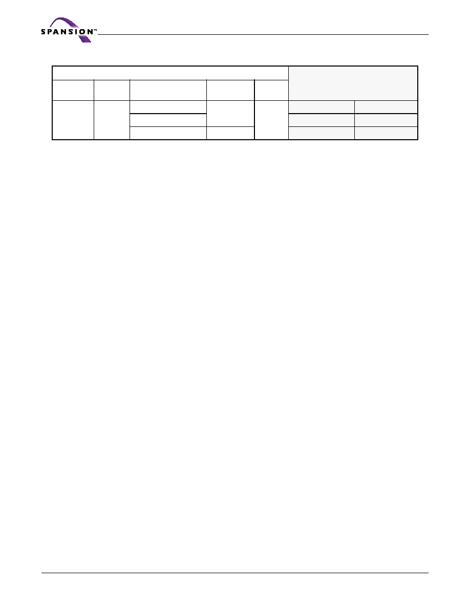
Table 6. S29GL032M (Model R0) Sector Address Table
Sector
A21
A20
A19
A18
A17
A16
8-bit Address Range
(in hexadecimal)
SA0
0
0
0
0
0
0
000000≠00FFFF
SA1
0
0
0
0
0
1
010000≠01FFFF
SA2
0
0
0
0
1
0
020000≠02FFFF
SA3
0
0
0
0
1
1
030000≠03FFFF
SA4
0
0
0
1
0
0
040000≠04FFFF
SA5
0
0
0
1
0
1
050000≠05FFFF
SA6
0
0
0
1
1
0
060000≠06FFFF
SA7
0
0
0
1
1
1
070000≠07FFFF
SA8
0
0
1
0
0
0
080000≠08FFFF
SA9
0
0
1
0
0
1
090000≠09FFFF
SA10
0
0
1
0
1
0
0A0000≠0AFFFF
SA11
0
0
1
0
1
1
0B0000≠0BFFFF
SA12
0
0
1
1
0
0
0C0000≠0CFFFF
SA13
0
0
1
1
0
1
0D0000≠0DFFFF
SA14
0
0
1
1
1
0
0E0000≠0EFFFF
SA15
0
0
1
1
1
1
0F0000≠0FFFFF
SA16
0
1
0
0
0
0
100000≠10FFFF
SA17
0
1
0
0
0
1
110000≠11FFFF
SA18
0
1
0
0
1
0
120000≠12FFFF
SA19
0
1
0
0
1
1
130000≠13FFFF
SA20
0
1
0
1
0
0
140000≠14FFFF
SA21
0
1
0
1
0
1
150000≠15FFFF
SA22
0
1
0
1
1
0
160000≠16FFFF
SA23
0
1
0
1
1
1
170000≠17FFFF
SA24
0
1
1
0
0
0
180000≠18FFFF
SA25
0
1
1
0
0
1
190000≠19FFFF
SA26
0
1
1
0
1
0
1A0000≠1AFFFF
SA27
0
1
1
0
1
1
1B0000≠1BFFFF
SA28
0
1
1
1
0
0
1C0000≠1CFFFF
SA29
0
1
1
1
0
1
1D0000≠1DFFFF
SA30
0
1
1
1
1
0
1E0000≠1EFFFF
SA31
0
1
1
1
1
1
1F0000≠1FFFFF

August 4, 2004 S29GLxxxM_00_B1_E
S29GLxxxM MirrorBit
TM
Flash Family
33
D a t a s h e e t
SA32
1
0
0
0
0
0
200000≠20FFFF
SA33
1
0
0
0
0
1
210000≠21FFFF
SA34
1
0
0
0
1
0
220000≠22FFFF
SA35
1
0
0
0
1
1
230000≠23FFFF
SA36
1
0
0
1
0
0
240000≠24FFFF
SA37
1
0
0
1
0
1
250000≠25FFFF
SA38
1
0
0
1
1
0
260000≠26FFFF
SA39
1
0
0
1
1
1
270000≠27FFFF
SA40
1
0
1
0
0
0
280000≠28FFFF
SA41
1
0
1
0
0
1
290000≠29FFFF
SA42
1
0
1
0
1
0
2A0000≠2AFFFF
SA43
1
0
1
0
1
1
2B0000≠2BFFFF
SA44
1
0
1
1
0
0
2C0000≠2CFFFF
SA45
1
0
1
1
0
1
2D0000≠2DFFFF
SA46
1
0
1
1
1
0
2E0000≠2EFFFF
SA47
1
0
1
1
1
1
2F0000≠2FFFFF
SA48
1
1
0
0
0
0
300000≠30FFFF
SA49
1
1
0
0
0
1
310000≠31FFFF
SA50
1
1
0
0
1
0
320000≠32FFFF
SA51
1
1
0
0
1
1
330000≠33FFFF
SA52
1
1
0
1
0
0
340000≠34FFFF
SA53
1
1
0
1
0
1
350000≠35FFFF
SA54
1
1
0
1
1
0
360000≠36FFFF
SA55
1
1
0
1
1
1
370000≠37FFFF
SA56
1
1
1
0
0
0
380000≠38FFFF
SA57
1
1
1
0
0
1
390000≠39FFFF
SA58
1
1
1
0
1
0
3A0000≠3AFFFF
SA59
1
1
1
0
1
1
3B0000≠3BFFFF
SA60
1
1
1
1
0
0
3C0000≠3CFFFF
SA61
1
1
1
1
0
1
3D0000≠3DFFFF
SA62
1
1
1
1
1
0
3E0000≠3EFFFF
SA63
1
1
1
1
1
1
3F0000≠3FFFFF
Table 6. S29GL032M (Model R0) Sector Address Table (Continued)
Sector
A21
A20
A19
A18
A17
A16
8-bit Address Range
(in hexadecimal)
34
S29GLxxxM MirrorBit
TM
Flash Family
S29GLxxxM_00_B1_E August 4, 2004
D a t a s h e e t
Table 7. S29GL032M (Models R1, R2) Sector Address Table
Sector
A20-A15
Sector Size
(Kbytes/Kwords)
8-bit
Address Range
(in hexadecimal)
16-bit
Address Range
(in hexadecimal)
SA0
0
0
0
0
0
0
64/32
000000≠00FFFF
000000≠007FFF
SA1
0
0
0
0
0
1
64/32
010000≠01FFFF
008000≠00FFFF
SA2
0
0
0
0
1
0
64/32
020000≠02FFFF
010000≠017FFF
SA3
0
0
0
0
1
1
64/32
030000≠03FFFF
018000≠01FFFF
SA4
0
0
0
1
0
0
64/32
040000≠04FFFF
020000≠027FFF
SA5
0
0
0
1
0
1
64/32
050000≠05FFFF
028000≠02FFFF
SA6
0
0
0
1
1
0
64/32
060000≠06FFFF
030000≠037FFF
SA7
0
0
0
1
1
1
64/32
070000≠07FFFF
038000≠03FFFF
SA8
0
0
1
0
0
0
64/32
080000≠08FFFF
040000≠047FFF
SA9
0
0
1
0
0
1
64/32
090000≠09FFFF
048000≠04FFFF
SA10
0
0
1
0
1
0
64/32
0A0000≠0AFFFF
050000≠057FFF
SA11
0
0
1
0
1
1
64/32
0B0000≠0BFFFF
058000≠05FFFF
SA12
0
0
1
1
0
0
64/32
0C0000≠0CFFFF
060000≠067FFF
SA13
0
0
1
1
0
1
64/32
0D0000≠0DFFFF
068000≠06FFFF
SA14
0
0
1
1
1
0
64/32
0E0000≠0EFFFF
070000≠077FFF
SA15
0
0
1
1
1
1
64/32
0F0000≠0FFFFF
078000≠07FFFF
SA16
0
1
0
0
0
0
64/32
100000≠10FFFF
080000≠087FFF
SA17
0
1
0
0
0
1
64/32
110000≠11FFFF
088000≠08FFFF
SA18
0
1
0
0
1
0
64/32
120000≠12FFFF
090000≠097FFF
SA19
0
1
0
0
1
1
64/32
130000≠13FFFF
098000≠09FFFF
SA20
0
1
0
1
0
0
64/32
140000≠14FFFF
0A0000≠0A7FFF
SA21
0
1
0
1
0
1
64/32
150000≠15FFFF
0A8000≠0AFFFF
SA22
0
1
0
1
1
0
64/32
160000≠16FFFF
0B0000≠0B7FFF
SA23
0
1
0
1
1
1
64/32
170000≠17FFFF
0B8000≠0BFFFF
SA24
0
1
1
0
0
0
64/32
180000≠18FFFF
0C0000≠0C7FFF
SA25
0
1
1
0
0
1
64/32
190000≠19FFFF
0C8000≠0CFFFF
SA26
0
1
1
0
1
0
64/32
1A0000≠1AFFFF
0D0000≠0D7FFF
SA27
0
1
1
0
1
1
64/32
1B0000≠1BFFFF
0D8000≠0DFFFF
SA28
0
1
1
1
0
0
64/32
1C0000≠1CFFFF
0E0000≠0E7FFF
SA29
0
1
1
1
0
1
64/32
1D0000≠1DFFFF
0E8000≠0EFFFF
SA30
0
1
1
1
1
0
64/32
1E0000≠1EFFFF
0F0000≠0F7FFF
SA31
0
1
1
1
1
1
64/32
1F0000≠1FFFFF
0F8000≠0FFFFF
SA32
1
0
0
0
0
0
64/32
200000≠20FFFF
100000≠107FFF
SA33
1
0
0
0
0
1
64/32
210000≠21FFFF
108000≠10FFFF
SA34
1
0
0
0
1
0
64/32
220000≠22FFFF
110000≠117FFF
SA35
1
0
0
0
1
1
64/32
230000≠23FFFF
118000≠11FFFF
SA36
1
0
0
1
0
0
64/32
240000≠24FFFF
120000≠127FFF
SA37
1
0
0
1
0
1
64/32
250000≠25FFFF
128000≠12FFFF
SA38
1
0
0
1
1
0
64/32
260000≠26FFFF
130000≠137FFF
SA39
1
0
0
1
1
1
64/32
270000≠27FFFF
138000≠13FFFF
SA40
1
0
1
0
0
0
64/32
280000≠28FFFF
140000≠147FFF
SA41
1
0
1
0
0
1
64/32
290000≠29FFFF
148000≠14FFFF
SA42
1
0
1
0
1
0
64/32
2A0000≠2AFFFF
150000≠157FFF
SA43
1
0
1
0
1
1
64/32
2B0000≠2BFFFF
158000≠15FFFF
SA44
1
0
1
1
0
0
64/32
2C0000≠2CFFFF
160000≠167FFF
August 4, 2004 S29GLxxxM_00_B1_E
S29GLxxxM MirrorBit
TM
Flash Family
35
D a t a s h e e t
SA45
1
0
1
1
0
1
64/32
2D0000≠2DFFFF
168000≠16FFFF
SA46
1
0
1
1
1
0
64/32
2E0000≠2EFFFF
170000≠177FFF
SA47
1
0
1
1
1
1
64/32
2F0000≠2FFFFF
178000≠17FFFF
SA48
1
1
0
0
0
0
64/32
300000≠30FFFF
180000≠187FFF
SA49
1
1
0
0
0
1
64/32
310000≠31FFFF
188000≠18FFFF
SA50
1
1
0
0
1
0
64/32
320000≠32FFFF
190000≠197FFF
SA51
1
1
0
0
1
1
64/32
330000≠33FFFF
198000≠19FFFF
SA52
1
1
0
1
0
0
64/32
340000≠34FFFF
1A0000≠1A7FFF
SA53
1
1
0
1
0
1
64/32
350000≠35FFFF
1A8000≠1AFFFF
SA54
1
1
0
1
1
0
64/32
360000≠36FFFF
1B0000≠1B7FFF
SA55
1
1
0
1
1
1
64/32
370000≠37FFFF
1B8000≠1BFFFF
SA56
1
1
1
0
0
0
64/32
380000≠38FFFF
1C0000≠1C7FFF
SA57
1
1
1
0
0
1
64/32
390000≠39FFFF
1C8000≠1CFFFF
SA58
1
1
1
0
1
0
64/32
3A0000≠3AFFFF
1D0000≠1D7FFF
SA59
1
1
1
0
1
1
64/32
3B0000≠3BFFFF
1D8000≠1DFFFF
SA60
1
1
1
1
0
0
64/32
3C0000≠3CFFFF
1E0000≠1E7FFF
SA61
1
1
1
1
0
1
64/32
3D0000≠3DFFFF
1E8000≠1EFFFF
SA62
1
1
1
1
1
0
64/32
3E0000≠3EFFFF
1F0000≠1F7FFF
SA63
1
1
1
1
1
1
64/32
3F0000≠3FFFFF
1F8000≠1FFFFF
Table 7. S29GL032M (Models R1, R2) Sector Address Table (Continued)
Sector
A20-A15
Sector Size
(Kbytes/Kwords)
8-bit
Address Range
(in hexadecimal)
16-bit
Address Range
(in hexadecimal)
36
S29GLxxxM MirrorBit
TM
Flash Family
S29GLxxxM_00_B1_E August 4, 2004
D a t a s h e e t
Table 8. S29GL032M (Model R3) Top Boot Sector Architecture
Sector
Sector Address
A20≠A12
Sector Size
(Kbytes/Kwords)
(x8)
Address Range
(x16)
Address Range
SA0
000000xxx
64/32
000000h≠00FFFFh
00000h≠07FFFh
SA1
000001xxx
64/32
010000h≠01FFFFh
08000h≠0FFFFh
SA2
000010xxx
64/32
020000h≠02FFFFh
10000h≠17FFFh
SA3
000011xxx
64/32
030000h≠03FFFFh
18000h≠1FFFFh
SA4
000100xxx
64/32
040000h≠04FFFFh
20000h≠27FFFh
SA5
000101xxx
64/32
050000h≠05FFFFh
28000h≠2FFFFh
SA6
000110xxx
64/32
060000h≠06FFFFh
30000h≠37FFFh
SA7
000111xxx
64/32
070000h≠07FFFFh
38000h≠3FFFFh
SA8
001000xxx
64/32
080000h≠08FFFFh
40000h≠47FFFh
SA9
001001xxx
64/32
090000h≠09FFFFh
48000h≠4FFFFh
SA10
001010xxx
64/32
0A0000h≠0AFFFFh
50000h≠57FFFh
SA11
001011xxx
64/32
0B0000h≠0BFFFFh
58000h≠5FFFFh
SA12
001100xxx
64/32
0C0000h≠0CFFFFh
60000h≠67FFFh
SA13
001101xxx
64/32
0D0000h≠0DFFFFh
68000h≠6FFFFh
SA14
001101xxx
64/32
0E0000h≠0EFFFFh
70000h≠77FFFh
SA15
001111xxx
64/32
0F0000h≠0FFFFFh
78000h≠7FFFFh
SA16
010000xxx
64/32
100000h≠00FFFFh
80000h≠87FFFh
SA17
010001xxx
64/32
110000h≠11FFFFh
88000h≠8FFFFh
SA18
010010xxx
64/32
120000h≠12FFFFh
90000h≠97FFFh
SA19
010011xxx
64/32
130000h≠13FFFFh
98000h≠9FFFFh
SA20
010100xxx
64/32
140000h≠14FFFFh
A0000h≠A7FFFh
SA21
010101xxx
64/32
150000h≠15FFFFh
A8000h≠AFFFFh
SA22
010110xxx
64/32
160000h≠16FFFFh
B0000h≠B7FFFh
SA23
010111xxx
64/32
170000h≠17FFFFh
B8000h≠BFFFFh
SA24
011000xxx
64/32
180000h≠18FFFFh
C0000h≠C7FFFh
SA25
011001xxx
64/32
190000h≠19FFFFh
C8000h≠CFFFFh
SA26
011010xxx
64/32
1A0000h≠1AFFFFh
D0000h≠D7FFFh
SA27
011011xxx
64/32
1B0000h≠1BFFFFh
D8000h≠DFFFFh
SA28
011000xxx
64/32
1C0000h≠1CFFFFh
E0000h≠E7FFFh
SA29
011101xxx
64/32
1D0000h≠1DFFFFh
E8000h≠EFFFFh
SA30
011110xxx
64/32
1E0000h≠1EFFFFh
F0000h≠F7FFFh
SA31
011111xxx
64/32
1F0000h≠1FFFFFh
F8000h≠FFFFFh
SA32
100000xxx
64/32
200000h≠20FFFFh
F9000h≠107FFFh
SA33
100001xxx
64/32
210000h≠21FFFFh
108000h≠10FFFFh
SA34
100010xxx
64/32
220000h≠22FFFFh
110000h≠117FFFh
SA35
101011xxx
64/32
230000h≠23FFFFh
118000h≠11FFFFh

August 4, 2004 S29GLxxxM_00_B1_E
S29GLxxxM MirrorBit
TM
Flash Family
37
D a t a s h e e t
SA36
100100xxx
64/32
240000h≠24FFFFh
120000h≠127FFFh
SA37
100101xxx
64/32
250000h≠25FFFFh
128000h≠12FFFFh
SA38
100110xxx
64/32
260000h≠26FFFFh
130000h≠137FFFh
SA39
100111xxx
64/32
270000h≠27FFFFh
138000h≠13FFFFh
SA40
101000xxx
64/32
280000h≠28FFFFh
140000h≠147FFFh
SA41
101001xxx
64/32
290000h≠29FFFFh
148000h≠14FFFFh
SA42
101010xxx
64/32
2A0000h≠2AFFFFh
150000h≠157FFFh
SA43
101011xxx
64/32
2B0000h≠2BFFFFh
158000h≠15FFFFh
SA44
101100xxx
64/32
2C0000h≠2CFFFFh
160000h≠167FFFh
SA45
101101xxx
64/32
2D0000h≠2DFFFFh
168000h≠16FFFFh
SA46
101110xxx
64/32
2E0000h≠2EFFFFh
170000h≠177FFFh
SA47
101111xxx
64/32
2F0000h≠2FFFFFh
178000h≠17FFFFh
SA48
110000xxx
64/32
300000h≠30FFFFh
180000h≠187FFFh
SA49
110001xxx
64/32
310000h≠31FFFFh
188000h≠18FFFFh
SA50
110010xxx
64/32
320000h≠32FFFFh
190000h≠197FFFh
SA51
110011xxx
64/32
330000h≠33FFFFh
198000h≠19FFFFh
SA52
100100xxx
64/32
340000h≠34FFFFh
1A0000h≠1A7FFFh
SA53
110101xxx
64/32
350000h≠35FFFFh
1A8000h≠1AFFFFh
SA54
110110xxx
64/32
360000h≠36FFFFh
1B0000h≠1B7FFFh
SA55
110111xxx
64/32
370000h≠37FFFFh
1B8000h≠1BFFFFh
SA56
111000xxx
64/32
380000h≠38FFFFh
1C0000h≠1C7FFFh
SA57
111001xxx
64/32
390000h≠39FFFFh
1C8000h≠1CFFFFh
SA58
111010xxx
64/32
3A0000h≠3AFFFFh
1D0000h≠1D7FFFh
SA59
111011xxx
64/32
3B0000h≠3BFFFFh
1D8000h≠1DFFFFh
SA60
111100xxx
64/32
3C0000h≠3CFFFFh
1E0000h≠1E7FFFh
SA61
111101xxx
64/32
3D0000h≠3DFFFFh
1E8000h≠1EFFFFh
SA62
111110xxx
64/32
3E0000h≠3EFFFFh
1F0000h≠1F7FFFh
SA63
111111000
8/4
3F0000h≠3F1FFFh
1F8000h≠1F8FFFh
SA64
111111001
8/4
3F2000h≠3F3FFFh
1F9000h≠1F9FFFh
SA65
111111010
8/4
3F4000h≠3F5FFFh
1FA000h≠1FAFFFh
SA66
111111011
8/4
3F6000h≠3F7FFFh
1FB000h≠1FBFFFh
SA67
111111100
8/4
3F8000h≠3F9FFFh
1FC000h≠1FCFFFh
SA68
111111101
8/4
3FA000h≠3FBFFFh
1FD000h≠1FDFFFh
SA69
111111110
8/4
3FC000h≠3FDFFFh
1FE000h≠1FEFFFh
SA70
111111111
8/4
3FE000h≠3FFFFFh
1FF000h≠1FFFFFh
Table 8. S29GL032M (Model R3) Top Boot Sector Architecture (Continued)
Sector
Sector Address
A20≠A12
Sector Size
(Kbytes/Kwords)
(x8)
Address Range
(x16)
Address Range

38
S29GLxxxM MirrorBit
TM
Flash Family
S29GLxxxM_00_B1_E August 4, 2004
D a t a s h e e t
Table 9. S29GL032M (Model R4) Bottom Boot Sector Architecture
Sector
Sector Address
A20≠A12
Sector Size
(Kbytes/Kwords)
(x8)
Address Range
(x16)
Address Range
SA0
000000000
8/4
000000h≠001FFFh
00000h≠00FFFh
SA1
000000001
8/4
002000h≠003FFFh
01000h≠01FFFh
SA2
000000010
8/4
004000h≠005FFFh
02000h≠02FFFh
SA3
000000011
8/4
006000h≠007FFFh
03000h≠03FFFh
SA4
000000100
8/4
008000h≠009FFFh
04000h≠04FFFh
SA5
000000101
8/4
00A000h≠00BFFFh
05000h≠05FFFh
SA6
000000110
8/4
00C000h≠00DFFFh
06000h≠06FFFh
SA7
000000111
8/4
00E000h≠00FFFFFh
07000h≠07FFFh
SA8
000001xxx
64/32
010000h≠01FFFFh
08000h≠0FFFFh
SA9
000010xxx
64/32
020000h≠02FFFFh
10000h≠17FFFh
SA10
000011xxx
64/32
030000h≠03FFFFh
18000h≠1FFFFh
SA11
000100xxx
64/32
040000h≠04FFFFh
20000h≠27FFFh
SA12
000101xxx
64/32
050000h≠05FFFFh
28000h≠2FFFFh
SA13
000110xxx
64/32
060000h≠06FFFFh
30000h≠37FFFh
SA14
000111xxx
64/32
070000h≠07FFFFh
38000h≠3FFFFh
SA15
001000xxx
64/32
080000h≠08FFFFh
40000h≠47FFFh
SA16
001001xxx
64/32
090000h≠09FFFFh
48000h≠4FFFFh
SA17
001010xxx
64/32
0A0000h≠0AFFFFh
50000h≠57FFFh
SA18
001011xxx
64/32
0B0000h≠0BFFFFh
58000h≠5FFFFh
SA19
001100xxx
64/32
0C0000h≠0CFFFFh
60000h≠67FFFh
SA20
001101xxx
64/32
0D0000h≠0DFFFFh
68000h≠6FFFFh
SA21
001101xxx
64/32
0E0000h≠0EFFFFh
70000h≠77FFFh
SA22
001111xxx
64/32
0F0000h≠0FFFFFh
78000h≠7FFFFh
SA23
010000xxx
64/32
100000h≠00FFFFh
80000h≠87FFFh
SA24
010001xxx
64/32
110000h≠11FFFFh
88000h≠8FFFFh
SA25
010010xxx
64/32
120000h≠12FFFFh
90000h≠97FFFh
SA26
010011xxx
64/32
130000h≠13FFFFh
98000h≠9FFFFh
SA27
010100xxx
64/32
140000h≠14FFFFh
A0000h≠A7FFFh
SA28
010101xxx
64/32
150000h≠15FFFFh
A8000h≠AFFFFh
SA29
010110xxx
64/32
160000h≠16FFFFh
B0000h≠B7FFFh
SA30
010111xxx
64/32
170000h≠17FFFFh
B8000h≠BFFFFh
SA31
011000xxx
64/32
180000h≠18FFFFh
C0000h≠C7FFFh
SA32
011001xxx
64/32
190000h≠19FFFFh
C8000h≠CFFFFh
SA33
011010xxx
64/32
1A0000h≠1AFFFFh
D0000h≠D7FFFh
SA34
011011xxx
64/32
1B0000h≠1BFFFFh
D8000h≠DFFFFh
SA35
011000xxx
64/32
1C0000h≠1CFFFFh
E0000h≠E7FFFh

August 4, 2004 S29GLxxxM_00_B1_E
S29GLxxxM MirrorBit
TM
Flash Family
39
D a t a s h e e t
SA36
011101xxx
64/32
1D0000h≠1DFFFFh
E8000h≠EFFFFh
SA37
011110xxx
64/32
1E0000h≠1EFFFFh
F0000h≠F7FFFh
SA38
011111xxx
64/32
1F0000h≠1FFFFFh
F8000h≠FFFFFh
SA39
100000xxx
64/32
200000h≠20FFFFh
F9000h≠107FFFh
SA40
100001xxx
64/32
210000h≠21FFFFh
108000h≠10FFFFh
SA41
100010xxx
64/32
220000h≠22FFFFh
110000h≠117FFFh
SA42
101011xxx
64/32
230000h≠23FFFFh
118000h≠11FFFFh
SA43
100100xxx
64/32
240000h≠24FFFFh
120000h≠127FFFh
SA44
100101xxx
64/32
250000h≠25FFFFh
128000h≠12FFFFh
SA45
100110xxx
64/32
260000h≠26FFFFh
130000h≠137FFFh
SA46
100111xxx
64/32
270000h≠27FFFFh
138000h≠13FFFFh
SA47
101000xxx
64/32
280000h≠28FFFFh
140000h≠147FFFh
SA48
101001xxx
64/32
290000h≠29FFFFh
148000h≠14FFFFh
SA49
101010xxx
64/32
2A0000h≠2AFFFFh
150000h≠157FFFh
SA50
101011xxx
64/32
2B0000h≠2BFFFFh
158000h≠15FFFFh
SA51
101100xxx
64/32
2C0000h≠2CFFFFh
160000h≠167FFFh
SA52
101101xxx
64/32
2D0000h≠2DFFFFh
168000h≠16FFFFh
SA53
101110xxx
64/32
2E0000h≠2EFFFFh
170000h≠177FFFh
SA54
101111xxx
64/32
2F0000h≠2FFFFFh
178000h≠17FFFFh
SA55
110000xxx
64/32
300000h≠30FFFFh
180000h≠187FFFh
SA56
110001xxx
64/32
310000h≠31FFFFh
188000h≠18FFFFh
SA57
110010xxx
64/32
320000h≠32FFFFh
190000h≠197FFFh
SA58
110011xxx
64/32
330000h≠33FFFFh
198000h≠19FFFFh
SA59
100100xxx
64/32
340000h≠34FFFFh
1A0000h≠1A7FFFh
SA60
110101xxx
64/32
350000h≠35FFFFh
1A8000h≠1AFFFFh
SA61
110110xxx
64/32
360000h≠36FFFFh
1B0000h≠1B7FFFh
SA62
110111xxx
64/32
370000h≠37FFFFh
1B8000h≠1BFFFFh
SA63
111000xxx
64/32
380000h≠38FFFFh
1C0000h≠1C7FFFh
SA64
111001xxx
64/32
390000h≠39FFFFh
1C8000h≠1CFFFFh
SA65
111010xxx
64/32
3A0000h≠3AFFFFh
1D0000h≠1D7FFFh
SA66
111011xxx
64/32
3B0000h≠3BFFFFh
1D8000h≠1DFFFFh
SA67
111100xxx
64/32
3C0000h≠3CFFFFh
1E0000h≠1E7FFFh
SA68
111101xxx
64/32
3D0000h≠3DFFFFh
1E8000h≠1EFFFFh
SA69
111110xxx
64/32
3E0000h≠3EFFFFh
1F0000h≠1F7FFFh
SA70
111111xxx
64/32
3F0000h≠3FFFFFh
1F8000h≠1FFFFFh
Table 9. S29GL032M (Model R4) Bottom Boot Sector Architecture (Continued)
Sector
Sector Address
A20≠A12
Sector Size
(Kbytes/Kwords)
(x8)
Address Range
(x16)
Address Range

40
S29GLxxxM MirrorBit
TM
Flash Family
S29GLxxxM_00_B1_E August 4, 2004
D a t a s h e e t
Table 10. S29GL064M (Model R0) Sector Address Table
Sector
A22
A21
A20
A19
A18
A17
A16
8-bit Address Range
(in hexadecimal)
SA0
0
0
0
0
0
0
0
000000≠00FFFF
SA1
0
0
0
0
0
0
1
010000≠01FFFF
SA2
0
0
0
0
0
1
0
020000≠02FFFF
SA3
0
0
0
0
0
1
1
030000≠03FFFF
SA4
0
0
0
0
1
0
0
040000≠04FFFF
SA5
0
0
0
0
1
0
1
050000≠05FFFF
SA6
0
0
0
0
1
1
0
060000≠06FFFF
SA7
0
0
0
0
1
1
1
070000≠07FFFF
SA8
0
0
0
1
0
0
0
080000≠08FFFF
SA9
0
0
0
1
0
0
1
090000≠09FFFF
SA10
0
0
0
1
0
1
0
0A0000≠0AFFFF
SA11
0
0
0
1
0
1
1
0B0000≠0BFFFF
SA12
0
0
0
1
1
0
0
0C0000≠0CFFFF
SA13
0
0
0
1
1
0
1
0D0000≠0DFFFF
SA14
0
0
0
1
1
1
0
0E0000≠0EFFFF
SA15
0
0
0
1
1
1
1
0F0000≠0FFFFF
SA16
0
0
1
0
0
0
0
100000≠10FFFF
SA17
0
0
1
0
0
0
1
110000≠11FFFF
SA18
0
0
1
0
0
1
0
120000≠12FFFF
SA19
0
0
1
0
0
1
1
130000≠13FFFF
SA20
0
0
1
0
1
0
0
140000≠14FFFF
SA21
0
0
1
0
1
0
1
150000≠15FFFF
SA22
0
0
1
0
1
1
0
160000≠16FFFF
SA23
0
0
1
0
1
1
1
170000≠17FFFF
SA24
0
0
1
1
0
0
0
180000≠18FFFF
SA25
0
0
1
1
0
0
1
190000≠19FFFF
SA26
0
0
1
1
0
1
0
1A0000≠1AFFFF
SA27
0
0
1
1
0
1
1
1B0000≠1BFFFF
SA28
0
0
1
1
1
0
0
1C0000≠1CFFFF
SA29
0
0
1
1
1
0
1
1D0000≠1DFFFF
SA30
0
0
1
1
1
1
0
1E0000≠1EFFFF
SA31
0
0
1
1
1
1
1
1F0000≠1FFFFF
SA32
0
1
0
0
0
0
0
200000≠20FFFF
SA33
0
1
0
0
0
0
1
210000≠21FFFF
SA34
0
1
0
0
0
1
0
220000≠22FFFF

August 4, 2004 S29GLxxxM_00_B1_E
S29GLxxxM MirrorBit
TM
Flash Family
41
D a t a s h e e t
SA35
0
1
0
0
0
1
1
230000≠23FFFF
SA36
0
1
0
0
1
0
0
240000≠24FFFF
SA37
0
1
0
0
1
0
1
250000≠25FFFF
SA38
0
1
0
0
1
1
0
260000≠26FFFF
SA39
0
1
0
0
1
1
1
270000≠27FFFF
SA40
0
1
0
1
0
0
0
280000≠28FFFF
SA41
0
1
0
1
0
0
1
290000≠29FFFF
SA42
0
1
0
1
0
1
0
2A0000≠2AFFFF
SA43
0
1
0
1
0
1
1
2B0000≠2BFFFF
SA44
0
1
0
1
1
0
0
2C0000≠2CFFFF
SA45
0
1
0
1
1
0
1
2D0000≠2DFFFF
SA46
0
1
0
1
1
1
0
2E0000≠2EFFFF
SA47
0
1
0
1
1
1
1
2F0000≠2FFFFF
SA48
0
1
1
0
0
0
0
300000≠30FFFF
SA49
0
1
1
0
0
0
1
310000≠31FFFF
SA50
0
1
1
0
0
1
0
320000≠32FFFF
SA51
0
1
1
0
0
1
1
330000≠33FFFF
SA52
0
1
1
0
1
0
0
340000≠34FFFF
SA53
0
1
1
0
1
0
1
350000≠35FFFF
SA54
0
1
1
0
1
1
0
360000≠36FFFF
SA55
0
1
1
0
1
1
1
370000≠37FFFF
SA56
0
1
1
1
0
0
0
380000≠38FFFF
SA57
0
1
1
1
0
0
1
390000≠39FFFF
SA58
0
1
1
1
0
1
0
3A0000≠3AFFFF
SA59
0
1
1
1
0
1
1
3B0000≠3BFFFF
SA60
0
1
1
1
1
0
0
3C0000≠3CFFFF
SA61
0
1
1
1
1
0
1
3D0000≠3DFFFF
SA62
0
1
1
1
1
1
0
3E0000≠3EFFFF
SA63
0
1
1
1
1
1
1
3F0000≠3FFFFF
SA64
1
0
0
0
0
0
0
400000≠40FFFF
SA65
1
0
0
0
0
0
1
410000≠41FFFF
SA66
1
0
0
0
0
1
0
420000≠42FFFF
SA67
1
0
0
0
0
1
1
430000≠43FFFF
SA68
1
0
0
0
1
0
0
440000≠44FFFF
SA69
1
0
0
0
1
0
1
450000≠45FFFF
Table 10. S29GL064M (Model R0) Sector Address Table (Continued)
Sector
A22
A21
A20
A19
A18
A17
A16
8-bit Address Range
(in hexadecimal)

42
S29GLxxxM MirrorBit
TM
Flash Family
S29GLxxxM_00_B1_E August 4, 2004
D a t a s h e e t
SA70
1
0
0
0
1
1
0
460000≠46FFFF
SA71
1
0
0
0
1
1
1
470000≠47FFFF
SA72
1
0
0
1
0
0
0
480000≠48FFFF
SA73
1
0
0
1
0
0
1
490000≠49FFFF
SA74
1
0
0
1
0
1
0
4A0000≠4AFFFF
SA75
1
0
0
1
0
1
1
4B0000≠4BFFFF
SA76
1
0
0
1
1
0
0
4C0000≠4CFFFF
SA77
1
0
0
1
1
0
1
4D0000≠4DFFFF
SA78
1
0
0
1
1
1
0
4E0000≠4EFFFF
SA79
1
0
0
1
1
1
1
4F0000≠4FFFFF
SA80
1
0
1
0
0
0
0
500000≠50FFFF
SA81
1
0
1
0
0
0
1
510000≠51FFFF
SA82
1
0
1
0
0
1
0
520000≠52FFFF
SA83
1
0
1
0
0
1
1
530000≠53FFFF
SA84
1
0
1
0
1
0
0
540000≠54FFFF
SA85
1
0
1
0
1
0
1
550000≠55FFFF
SA86
1
0
1
0
1
1
0
560000≠56FFFF
SA87
1
0
1
0
1
1
1
570000≠57FFFF
SA88
1
0
1
1
0
0
0
580000≠58FFFF
SA89
1
0
1
1
0
0
1
590000≠59FFFF
SA90
1
0
1
1
0
1
0
5A0000≠5AFFFF
SA91
1
0
1
1
0
1
1
5B0000≠5BFFFF
SA92
1
0
1
1
1
0
0
5C0000≠5CFFFF
SA93
1
0
1
1
1
0
1
5D0000≠5DFFFF
SA94
1
0
1
1
1
1
0
5E0000≠5EFFFF
SA95
1
0
1
1
1
1
1
5F0000≠5FFFFF
SA96
1
1
0
0
0
0
0
600000≠60FFFF
SA97
1
1
0
0
0
0
1
610000≠61FFFF
SA98
1
1
0
0
0
1
0
620000≠62FFFF
SA99
1
1
0
0
0
1
1
630000≠63FFFF
SA100
1
1
0
0
1
0
0
640000≠64FFFF
SA101
1
1
0
0
1
0
1
650000≠65FFFF
SA102
1
1
0
0
1
1
0
660000≠66FFFF
SA103
1
1
0
0
1
1
1
670000≠67FFFF
SA104
1
1
0
1
0
0
0
680000≠68FFFF
Table 10. S29GL064M (Model R0) Sector Address Table (Continued)
Sector
A22
A21
A20
A19
A18
A17
A16
8-bit Address Range
(in hexadecimal)

August 4, 2004 S29GLxxxM_00_B1_E
S29GLxxxM MirrorBit
TM
Flash Family
43
D a t a s h e e t
SA105
1
1
0
1
0
0
1
690000≠69FFFF
SA106
1
1
0
1
0
1
0
6A0000≠6AFFFF
SA107
1
1
0
1
0
1
1
6B0000≠6BFFFF
SA108
1
1
0
1
1
0
0
6C0000≠6CFFFF
SA109
1
1
0
1
1
0
1
6D0000≠6DFFFF
SA110
1
1
0
1
1
1
0
6E0000≠6EFFFF
SA111
1
1
0
1
1
1
1
6F0000≠6FFFFF
SA112
1
1
1
0
0
0
0
700000≠70FFFF
SA113
1
1
1
0
0
0
1
710000≠71FFFF
SA114
1
1
1
0
0
1
0
720000≠72FFFF
SA115
1
1
1
0
0
1
1
730000≠73FFFF
SA116
1
1
1
0
1
0
0
740000≠74FFFF
SA117
1
1
1
0
1
0
1
750000≠75FFFF
SA118
1
1
1
0
1
1
0
760000≠76FFFF
SA119
1
1
1
0
1
1
1
770000≠77FFFF
SA120
1
1
1
1
0
0
0
780000≠78FFFF
SA121
1
1
1
1
0
0
1
790000≠79FFFF
SA122
1
1
1
1
0
1
0
7A0000≠7AFFFF
SA123
1
1
1
1
0
1
1
7B0000≠7BFFFF
SA124
1
1
1
1
1
0
0
7C0000≠7CFFFF
SA125
1
1
1
1
1
0
1
7D0000≠7DFFFF
SA126
1
1
1
1
1
1
0
7E0000≠7EFFFF
SA127
1
1
1
1
1
1
1
7F0000≠7FFFFF
Table 10. S29GL064M (Model R0) Sector Address Table (Continued)
Sector
A22
A21
A20
A19
A18
A17
A16
8-bit Address Range
(in hexadecimal)

44
S29GLxxxM MirrorBit
TM
Flash Family
S29GLxxxM_00_B1_E August 4, 2004
D a t a s h e e t
Table 11. S29GL064M (Model R1, R2) Sector Address Table
Sector
A21≠A15
Sector Size
(Kbytes/
Kwords)
8-bit
Address Range
(in
hexadecimal)
16-bit
Address Range
(in
hexadecimal)
SA0
0
0
0
0
0
0
0
64/32
000000≠00FFFF
000000≠007FFF
SA1
0
0
0
0
0
0
1
64/32
010000≠01FFFF
008000≠00FFFF
SA2
0
0
0
0
0
1
0
64/32
020000≠02FFFF
010000≠017FFF
SA3
0
0
0
0
0
1
1
64/32
030000≠03FFFF
018000≠01FFFF
SA4
0
0
0
0
1
0
0
64/32
040000≠04FFFF
020000≠027FFF
SA5
0
0
0
0
1
0
1
64/32
050000≠05FFFF
028000≠02FFFF
SA6
0
0
0
0
1
1
0
64/32
060000≠06FFFF
030000≠037FFF
SA7
0
0
0
0
1
1
1
64/32
070000≠07FFFF
038000≠03FFFF
SA8
0
0
0
1
0
0
0
64/32
080000≠08FFFF
040000≠047FFF
SA9
0
0
0
1
0
0
1
64/32
090000≠09FFFF
048000≠04FFFF
SA10
0
0
0
1
0
1
0
64/32
0A0000≠0AFFFF
050000≠057FFF
SA11
0
0
0
1
0
1
1
64/32
0B0000≠0BFFFF
058000≠05FFFF
SA12
0
0
0
1
1
0
0
64/32
0C0000≠0CFFFF
060000≠067FFF
SA13
0
0
0
1
1
0
1
64/32
0D0000≠0DFFFF
068000≠06FFFF
SA14
0
0
0
1
1
1
0
64/32
0E0000≠0EFFFF
070000≠077FFF
SA15
0
0
0
1
1
1
1
64/32
0F0000≠0FFFFF
078000≠07FFFF
SA16
0
0
1
0
0
0
0
64/32
100000≠10FFFF
080000≠087FFF
SA17
0
0
1
0
0
0
1
64/32
110000≠11FFFF
088000≠08FFFF
SA18
0
0
1
0
0
1
0
64/32
120000≠12FFFF
090000≠097FFF
SA19
0
0
1
0
0
1
1
64/32
130000≠13FFFF
098000≠09FFFF
SA20
0
0
1
0
1
0
0
64/32
140000≠14FFFF
0A0000≠0A7FFF
SA21
0
0
1
0
1
0
1
64/32
150000≠15FFFF
0A8000≠0AFFFF
SA22
0
0
1
0
1
1
0
64/32
160000≠16FFFF
0B0000≠0B7FFF
SA23
0
0
1
0
1
1
1
64/32
170000≠17FFFF
0B8000≠0BFFFF
SA24
0
0
1
1
0
0
0
64/32
180000≠18FFFF
0C0000≠0C7FFF
SA25
0
0
1
1
0
0
1
64/32
190000≠19FFFF
0C8000≠0CFFFF
SA26
0
0
1
1
0
1
0
64/32
1A0000≠1AFFFF
0D0000≠0D7FFF
SA27
0
0
1
1
0
1
1
64/32
1B0000≠1BFFFF
0D8000≠0DFFFF
SA28
0
0
1
1
1
0
0
64/32
1C0000≠1CFFFF
0E0000≠0E7FFF
SA29
0
0
1
1
1
0
1
64/32
1D0000≠1DFFFF
0E8000≠0EFFFF
SA30
0
0
1
1
1
1
0
64/32
1E0000≠1EFFFF
0F0000≠0F7FFF
SA31
0
0
1
1
1
1
1
64/32
1F0000≠1FFFFF
0F8000≠0FFFFF
SA32
0
1
0
0
0
0
0
64/32
200000≠20FFFF
100000≠107FFF
SA33
0
1
0
0
0
0
1
64/32
210000≠21FFFF
108000≠10FFFF
August 4, 2004 S29GLxxxM_00_B1_E
S29GLxxxM MirrorBit
TM
Flash Family
45
D a t a s h e e t
SA34
0
1
0
0
0
1
0
64/32
220000≠22FFFF
110000≠117FFF
SA35
0
1
0
0
0
1
1
64/32
230000≠23FFFF
118000≠11FFFF
SA36
0
1
0
0
1
0
0
64/32
240000≠24FFFF
120000≠127FFF
SA37
0
1
0
0
1
0
1
64/32
250000≠25FFFF
128000≠12FFFF
SA38
0
1
0
0
1
1
0
64/32
260000≠26FFFF
130000≠137FFF
SA39
0
1
0
0
1
1
1
64/32
270000≠27FFFF
138000≠13FFFF
SA40
0
1
0
1
0
0
0
64/32
280000≠28FFFF
140000≠147FFF
SA41
0
1
0
1
0
0
1
64/32
290000≠29FFFF
148000≠14FFFF
SA42
0
1
0
1
0
1
0
64/32
2A0000≠2AFFFF
150000≠157FFF
SA43
0
1
0
1
0
1
1
64/32
2B0000≠2BFFFF
158000≠15FFFF
SA44
0
1
0
1
1
0
0
64/32
2C0000≠2CFFFF
160000≠167FFF
SA45
0
1
0
1
1
0
1
64/32
2D0000≠2DFFFF
168000≠16FFFF
SA46
0
1
0
1
1
1
0
64/32
2E0000≠2EFFFF
170000≠177FFF
SA47
0
1
0
1
1
1
1
64/32
2F0000≠2FFFFF
178000≠17FFFF
SA48
0
1
1
0
0
0
0
64/32
300000≠30FFFF
180000≠187FFF
SA49
0
1
1
0
0
0
1
64/32
310000≠31FFFF
188000≠18FFFF
SA50
0
1
1
0
0
1
0
64/32
320000≠32FFFF
190000≠197FFF
SA51
0
1
1
0
0
1
1
64/32
330000≠33FFFF
198000≠19FFFF
SA52
0
1
1
0
1
0
0
64/32
340000≠34FFFF
1A0000≠1A7FFF
SA53
0
1
1
0
1
0
1
64/32
350000≠35FFFF
1A8000≠1AFFFF
SA54
0
1
1
0
1
1
0
64/32
360000≠36FFFF
1B0000≠1B7FFF
SA55
0
1
1
0
1
1
1
64/32
370000≠37FFFF
1B8000≠1BFFFF
SA56
0
1
1
1
0
0
0
64/32
380000≠38FFFF
1C0000≠1C7FFF
SA57
0
1
1
1
0
0
1
64/32
390000≠39FFFF
1C8000≠1CFFFF
SA58
0
1
1
1
0
1
0
64/32
3A0000≠3AFFFF
1D0000≠1D7FFF
SA59
0
1
1
1
0
1
1
64/32
3B0000≠3BFFFF
1D8000≠1DFFFF
SA60
0
1
1
1
1
0
0
64/32
3C0000≠3CFFFF
1E0000≠1E7FFF
SA61
0
1
1
1
1
0
1
64/32
3D0000≠3DFFFF
1E8000≠1EFFFF
SA62
0
1
1
1
1
1
0
64/32
3E0000≠3EFFFF
1F0000≠1F7FFF
SA63
0
1
1
1
1
1
1
64/32
3F0000≠3FFFFF
1F8000≠1FFFFF
SA64
1
0
0
0
0
0
0
64/32
400000≠40FFFF
200000≠207FFF
SA65
1
0
0
0
0
0
1
64/32
410000≠41FFFF
208000≠20FFFF
SA66
1
0
0
0
0
1
0
64/32
420000≠42FFFF
210000≠217FFF
SA67
1
0
0
0
0
1
1
64/32
430000≠43FFFF
218000≠21FFFF
SA68
1
0
0
0
1
0
0
64/32
440000≠44FFFF
220000≠227FFF
Table 11. S29GL064M (Model R1, R2) Sector Address Table (Continued)
Sector
A21≠A15
Sector Size
(Kbytes/
Kwords)
8-bit
Address Range
(in
hexadecimal)
16-bit
Address Range
(in
hexadecimal)

46
S29GLxxxM MirrorBit
TM
Flash Family
S29GLxxxM_00_B1_E August 4, 2004
D a t a s h e e t
SA69
1
0
0
0
1
0
1
64/32
450000≠45FFFF
228000≠22FFFF
SA70
1
0
0
0
1
1
0
64/32
460000≠46FFFF
230000≠237FFF
SA71
1
0
0
0
1
1
1
64/32
470000≠47FFFF
238000≠23FFFF
SA72
1
0
0
1
0
0
0
64/32
480000≠48FFFF
240000≠247FFF
SA73
1
0
0
1
0
0
1
64/32
490000≠49FFFF
248000≠24FFFF
SA74
1
0
0
1
0
1
0
64/32
4A0000≠4AFFFF
250000≠257FFF
SA75
1
0
0
1
0
1
1
64/32
4B0000≠4BFFFF
258000≠25FFFF
SA76
1
0
0
1
1
0
0
64/32
4C0000≠4CFFFF
260000≠267FFF
SA77
1
0
0
1
1
0
1
64/32
4D0000≠4DFFFF
268000≠26FFFF
SA78
1
0
0
1
1
1
0
64/32
4E0000≠4EFFFF
270000≠277FFF
SA79
1
0
0
1
1
1
1
64/32
4F0000≠4FFFFF
278000≠27FFFF
SA80
1
0
1
0
0
0
0
64/32
500000≠50FFFF
280000≠287FFF
SA81
1
0
1
0
0
0
1
64/32
510000≠51FFFF
288000≠28FFFF
SA82
1
0
1
0
0
1
0
64/32
520000≠52FFFF
290000≠297FFF
SA83
1
0
1
0
0
1
1
64/32
530000≠53FFFF
298000≠29FFFF
SA84
1
0
1
0
1
0
0
64/32
540000≠54FFFF
2A0000≠2A7FFF
SA85
1
0
1
0
1
0
1
64/32
550000≠55FFFF
2A8000≠2AFFFF
SA86
1
0
1
0
1
1
0
64/32
560000≠56FFFF
2B0000≠2B7FFF
SA87
1
0
1
0
1
1
1
64/32
570000≠57FFFF
2B8000≠2BFFFF
SA88
1
0
1
1
0
0
0
64/32
580000≠58FFFF
2C0000≠2C7FFF
SA89
1
0
1
1
0
0
1
64/32
590000≠59FFFF
2C8000≠2CFFFF
SA90
1
0
1
1
0
1
0
64/32
5A0000≠5AFFFF
2D0000≠2D7FFF
SA91
1
0
1
1
0
1
1
64/32
5B0000≠5BFFFF
2D8000≠2DFFFF
SA92
1
0
1
1
1
0
0
64/32
5C0000≠5CFFFF
2E0000≠2E7FFF
SA93
1
0
1
1
1
0
1
64/32
5D0000≠5DFFFF
2E8000≠2EFFFF
SA94
1
0
1
1
1
1
0
64/32
5E0000≠5EFFFF
2F0000≠2F7FFF
SA95
1
0
1
1
1
1
1
64/32
5F0000≠5FFFFF
2F8000≠2FFFFF
SA96
1
1
0
0
0
0
0
64/32
600000≠60FFFF
300000≠307FFF
SA97
1
1
0
0
0
0
1
64/32
610000≠61FFFF
308000≠30FFFF
SA98
1
1
0
0
0
1
0
64/32
620000≠62FFFF
310000≠317FFF
SA99
1
1
0
0
0
1
1
64/32
630000≠63FFFF
318000≠31FFFF
SA100
1
1
0
0
1
0
0
64/32
640000≠64FFFF
320000≠327FFF
SA101
1
1
0
0
1
0
1
64/32
650000≠65FFFF
328000≠32FFFF
SA102
1
1
0
0
1
1
0
64/32
660000≠66FFFF
330000≠337FFF
SA103
1
1
0
0
1
1
1
64/32
670000≠67FFFF
338000≠33FFFF
Table 11. S29GL064M (Model R1, R2) Sector Address Table (Continued)
Sector
A21≠A15
Sector Size
(Kbytes/
Kwords)
8-bit
Address Range
(in
hexadecimal)
16-bit
Address Range
(in
hexadecimal)
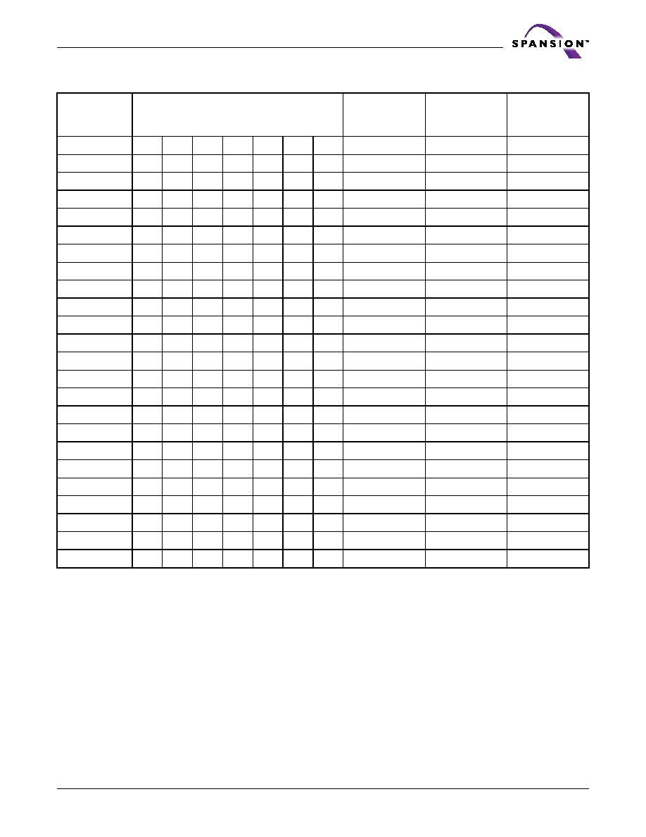
August 4, 2004 S29GLxxxM_00_B1_E
S29GLxxxM MirrorBit
TM
Flash Family
47
D a t a s h e e t
SA104
1
1
0
1
0
0
0
64/32
680000≠68FFFF
340000≠347FFF
SA105
1
1
0
1
0
0
1
64/32
690000≠69FFFF
348000≠34FFFF
SA106
1
1
0
1
0
1
0
64/32
6A0000≠6AFFFF
350000≠357FFF
SA107
1
1
0
1
0
1
1
64/32
6B0000≠6BFFFF
358000≠35FFFF
SA108
1
1
0
1
1
0
0
64/32
6C0000≠6CFFFF
360000≠367FFF
SA109
1
1
0
1
1
0
1
64/32
6D0000≠6DFFFF
368000≠36FFFF
SA110
1
1
0
1
1
1
0
64/32
6E0000≠6EFFFF
370000≠377FFF
SA111
1
1
0
1
1
1
1
64/32
6F0000≠6FFFFF
378000≠37FFFF
SA112
1
1
1
0
0
0
0
64/32
700000≠70FFFF
380000≠387FFF
SA113
1
1
1
0
0
0
1
64/32
710000≠71FFFF
388000≠38FFFF
SA114
1
1
1
0
0
1
0
64/32
720000≠72FFFF
390000≠397FFF
SA115
1
1
1
0
0
1
1
64/32
730000≠73FFFF
398000≠39FFFF
SA116
1
1
1
0
1
0
0
64/32
740000≠74FFFF
3A0000≠3A7FFF
SA117
1
1
1
0
1
0
1
64/32
750000≠75FFFF
3A8000≠3AFFFF
SA118
1
1
1
0
1
1
0
64/32
760000≠76FFFF
3B0000≠3B7FFF
SA119
1
1
1
0
1
1
1
64/32
770000≠77FFFF
3B8000≠3BFFFF
SA120
1
1
1
1
0
0
0
64/32
780000≠78FFFF
3C0000≠3C7FFF
SA121
1
1
1
1
0
0
1
64/32
790000≠79FFFF
3C8000≠3CFFFF
SA122
1
1
1
1
0
1
0
64/32
7A0000≠7AFFFF
3D0000≠3D7FFF
SA123
1
1
1
1
0
1
1
64/32
7B0000≠7BFFFF
3D8000≠3DFFFF
SA124
1
1
1
1
1
0
0
64/32
7C0000≠7CFFFF
3E0000≠3E7FFF
SA125
1
1
1
1
1
0
1
64/32
7D0000≠7DFFFF
3E8000≠3EFFFF
SA126
1
1
1
1
1
1
0
64/32
7E0000≠7EFFFF
3F0000≠3F7FFF
SA127
1
1
1
1
1
1
1
64/32
7F0000≠7FFFFF
3F8000≠3FFFFF
Table 11. S29GL064M (Model R1, R2) Sector Address Table (Continued)
Sector
A21≠A15
Sector Size
(Kbytes/
Kwords)
8-bit
Address Range
(in
hexadecimal)
16-bit
Address Range
(in
hexadecimal)

48
S29GLxxxM MirrorBit
TM
Flash Family
S29GLxxxM_00_B1_E August 4, 2004
D a t a s h e e t
Table 12. S29GL064M (Model R3) Top Boot Sector Architecture
Sector
Sector Address
A21≠A12
Sector Size
(Kbytes/Kwords)
(x8)
Address Range
(x16)
Address Range
SA0
0000000xxx
64/32
000000h≠00FFFFh
00000h≠07FFFh
SA1
0000001xxx
64/32
010000h≠01FFFFh
08000h≠0FFFFh
SA2
0000010xxx
64/32
020000h≠02FFFFh
10000h≠17FFFh
SA3
0000011xxx
64/32
030000h≠03FFFFh
18000h≠1FFFFh
SA4
0000100xxx
64/32
040000h≠04FFFFh
20000h≠27FFFh
SA5
0000101xxx
64/32
050000h≠05FFFFh
28000h≠2FFFFh
SA6
0000110xxx
64/32
060000h≠06FFFFh
30000h≠37FFFh
SA7
0000111xxx
64/32
070000h≠07FFFFh
38000h≠3FFFFh
SA8
0001000xxx
64/32
080000h≠08FFFFh
40000h≠47FFFh
SA9
0001001xxx
64/32
090000h≠09FFFFh
48000h≠4FFFFh
SA10
0001010xxx
64/32
0A0000h≠0AFFFFh
50000h≠57FFFh
SA11
0001011xxx
64/32
0B0000h≠0BFFFFh
58000h≠5FFFFh
SA12
0001100xxx
64/32
0C0000h≠0CFFFFh
60000h≠67FFFh
SA13
0001101xxx
64/32
0D0000h≠0DFFFFh
68000h≠6FFFFh
SA14
0001101xxx
64/32
0E0000h≠0EFFFFh
70000h≠77FFFh
SA15
0001111xxx
64/32
0F0000h≠0FFFFFh
78000h≠7FFFFh
SA16
0010000xxx
64/32
100000h≠00FFFFh
80000h≠87FFFh
SA17
0010001xxx
64/32
110000h≠11FFFFh
88000h≠8FFFFh
SA18
0010010xxx
64/32
120000h≠12FFFFh
90000h≠97FFFh
SA19
0010011xxx
64/32
130000h≠13FFFFh
98000h≠9FFFFh
SA20
0010100xxx
64/32
140000h≠14FFFFh
A0000h≠A7FFFh
SA21
0010101xxx
64/32
150000h≠15FFFFh
A8000h≠AFFFFh
SA22
0010110xxx
64/32
160000h≠16FFFFh
B0000h≠B7FFFh
SA23
0010111xxx
64/32
170000h≠17FFFFh
B8000h≠BFFFFh
SA24
0011000xxx
64/32
180000h≠18FFFFh
C0000h≠C7FFFh
SA25
0011001xxx
64/32
190000h≠19FFFFh
C8000h≠CFFFFh
SA26
0011010xxx
64/32
1A0000h≠1AFFFFh
D0000h≠D7FFFh
SA27
0011011xxx
64/32
1B0000h≠1BFFFFh
D8000h≠DFFFFh
SA28
0011000xxx
64/32
1C0000h≠1CFFFFh
E0000h≠E7FFFh
SA29
0011101xxx
64/32
1D0000h≠1DFFFFh
E8000h≠EFFFFh
SA30
0011110xxx
64/32
1E0000h≠1EFFFFh
F0000h≠F7FFFh
SA31
0011111xxx
64/32
1F0000h≠1FFFFFh
F8000h≠FFFFFh
SA32
0100000xxx
64/32
200000h≠20FFFFh
F9000h≠107FFFh
SA33
0100001xxx
64/32
210000h≠21FFFFh
108000h≠10FFFFh
SA34
0100010xxx
64/32
220000h≠22FFFFh
110000h≠117FFFh
SA35
0101011xxx
64/32
230000h≠23FFFFh
118000h≠11FFFFh
August 4, 2004 S29GLxxxM_00_B1_E
S29GLxxxM MirrorBit
TM
Flash Family
49
D a t a s h e e t
SA36
0100100xxx
64/32
240000h≠24FFFFh
120000h≠127FFFh
SA37
0100101xxx
64/32
250000h≠25FFFFh
128000h≠12FFFFh
SA38
0100110xxx
64/32
260000h≠26FFFFh
130000h≠137FFFh
SA39
0100111xxx
64/32
270000h≠27FFFFh
138000h≠13FFFFh
SA40
0101000xxx
64/32
280000h≠28FFFFh
140000h≠147FFFh
SA41
0101001xxx
64/32
290000h≠29FFFFh
148000h≠14FFFFh
SA42
0101010xxx
64/32
2A0000h≠2AFFFFh
150000h≠157FFFh
SA43
0101011xxx
64/32
2B0000h≠2BFFFFh
158000h≠15FFFFh
SA44
0101100xxx
64/32
2C0000h≠2CFFFFh
160000h≠167FFFh
SA45
0101101xxx
64/32
2D0000h≠2DFFFFh
168000h≠16FFFFh
SA46
0101110xxx
64/32
2E0000h≠2EFFFFh
170000h≠177FFFh
SA47
0101111xxx
64/32
2F0000h≠2FFFFFh
178000h≠17FFFFh
SA48
0110000xxx
64/32
300000h≠30FFFFh
180000h≠187FFFh
SA49
0110001xxx
64/32
310000h≠31FFFFh
188000h≠18FFFFh
SA50
0110010xxx
64/32
320000h≠32FFFFh
190000h≠197FFFh
SA51
0110011xxx
64/32
330000h≠33FFFFh
198000h≠19FFFFh
SA52
0100100xxx
64/32
340000h≠34FFFFh
1A0000h≠1A7FFFh
SA53
0110101xxx
64/32
350000h≠35FFFFh
1A8000h≠1AFFFFh
SA54
0110110xxx
64/32
360000h≠36FFFFh
1B0000h≠1B7FFFh
SA55
0110111xxx
64/32
370000h≠37FFFFh
1B8000h≠1BFFFFh
SA56
0111000xxx
64/32
380000h≠38FFFFh
1C0000h≠1C7FFFh
SA57
0111001xxx
64/32
390000h≠39FFFFh
1C8000h≠1CFFFFh
SA58
0111010xxx
64/32
3A0000h≠3AFFFFh
1D0000h≠1D7FFFh
SA59
0111011xxx
64/32
3B0000h≠3BFFFFh
1D8000h≠1DFFFFh
SA60
0111100xxx
64/32
3C0000h≠3CFFFFh
1E0000h≠1E7FFFh
SA61
0111101xxx
64/32
3D0000h≠3DFFFFh
1E8000h≠1EFFFFh
SA62
0111110xxx
64/32
3E0000h≠3EFFFFh
1F0000h≠1F7FFFh
SA63
0111111xxx
64/32
3F0000h≠3FFFFFh
1F8000h≠1FFFFFh
SA64
1000000xxx
64/32
400000h≠40FFFFh
200000h≠207FFFh
SA65
1000001xxx
64/32
410000h≠41FFFFh
208000h≠20FFFFh
SA66
1000010xxx
64/32
420000h≠42FFFFh
210000h≠217FFFh
SA67
1000011xxx
64/32
430000h≠43FFFFh
218000h≠21FFFFh
SA68
1000100xxx
64/32
440000h≠44FFFFh
220000h≠227FFFh
SA69
1000101xxx
64/32
450000h≠45FFFFh
228000h≠22FFFFh
SA70
1000110xxx
64/32
460000h≠46FFFFh
230000h≠237FFFh
SA71
1000111xxx
64/32
470000h≠47FFFFh
238000h≠23FFFFh
Table 12. S29GL064M (Model R3) Top Boot Sector Architecture (Continued)
Sector
Sector Address
A21≠A12
Sector Size
(Kbytes/Kwords)
(x8)
Address Range
(x16)
Address Range
50
S29GLxxxM MirrorBit
TM
Flash Family
S29GLxxxM_00_B1_E August 4, 2004
D a t a s h e e t
SA72
1001000xxx
64/32
480000h≠48FFFFh
240000h≠247FFFh
SA73
1001001xxx
64/32
490000h≠49FFFFh
248000h≠24FFFFh
SA74
1001010xxx
64/32
4A0000h≠4AFFFFh
250000h≠257FFFh
SA75
1001011xxx
64/32
4B0000h≠4BFFFFh
258000h≠25FFFFh
SA76
1001100xxx
64/32
4C0000h≠4CFFFFh
260000h≠267FFFh
SA77
1001101xxx
64/32
4D0000h≠4DFFFFh
268000h≠26FFFFh
SA78
1001110xxx
64/32
4E0000h≠4EFFFFh
270000h≠277FFFh
SA79
1001111xxx
64/32
4F0000h≠4FFFFFh
278000h≠27FFFFh
SA80
1010000xxx
64/32
500000h≠50FFFFh
280000h≠28FFFFh
SA81
1010001xxx
64/32
510000h≠51FFFFh
288000h≠28FFFFh
SA82
1010010xxx
64/32
520000h≠52FFFFh
290000h≠297FFFh
SA83
1010011xxx
64/32
530000h≠53FFFFh
298000h≠29FFFFh
SA84
1010100xxx
64/32
540000h≠54FFFFh
2A0000h≠2A7FFFh
SA85
1010101xxx
64/32
550000h≠55FFFFh
2A8000h≠2AFFFFh
SA86
1010110xxx
64/32
560000h≠56FFFFh
2B0000h≠2B7FFFh
SA87
1010111xxx
64/32
570000h≠57FFFFh
2B8000h≠2BFFFFh
SA88
1011000xxx
64/32
580000h≠58FFFFh
2C0000h≠2C7FFFh
SA89
1011001xxx
64/32
590000h≠59FFFFh
2C8000h≠2CFFFFh
SA90
1011010xxx
64/32
5A0000h≠5AFFFFh
2D0000h≠2D7FFFh
SA91
1011011xxx
64/32
5B0000h≠5BFFFFh
2D8000h≠2DFFFFh
SA92
1011100xxx
64/32
5C0000h≠5CFFFFh
2E0000h≠2E7FFFh
SA93
1011101xxx
64/32
5D0000h≠5DFFFFh
2E8000h≠2EFFFFh
SA94
1011110xxx
64/32
5E0000h≠5EFFFFh
2F0000h≠2FFFFFh
SA95
1011111xxx
64/32
5F0000h≠5FFFFFh
2F8000h≠2FFFFFh
SA96
1100000xxx
64/32
600000h≠60FFFFh
300000h≠307FFFh
SA97
1100001xxx
64/32
610000h≠61FFFFh
308000h≠30FFFFh
SA98
1100010xxx
64/32
620000h≠62FFFFh
310000h≠317FFFh
SA99
1100011xxx
64/32
630000h≠63FFFFh
318000h≠31FFFFh
SA100
1100100xxx
64/32
640000h≠64FFFFh
320000h≠327FFFh
SA101
1100101xxx
64/32
650000h≠65FFFFh
328000h≠32FFFFh
SA102
1100110xxx
64/32
660000h≠66FFFFh
330000h≠337FFFh
SA103
1100111xxx
64/32
670000h≠67FFFFh
338000h≠33FFFFh
SA104
1101000xxx
64/32
680000h≠68FFFFh
340000h≠347FFFh
SA105
1101001xxx
64/32
690000h≠69FFFFh
348000h≠34FFFFh
SA106
1101010xxx
64/32
6A0000h≠6AFFFFh
350000h≠357FFFh
SA107
1101011xxx
64/32
6B0000h≠6BFFFFh
358000h≠35FFFFh
Table 12. S29GL064M (Model R3) Top Boot Sector Architecture (Continued)
Sector
Sector Address
A21≠A12
Sector Size
(Kbytes/Kwords)
(x8)
Address Range
(x16)
Address Range

August 4, 2004 S29GLxxxM_00_B1_E
S29GLxxxM MirrorBit
TM
Flash Family
51
D a t a s h e e t
SA108
1101100xxx
64/32
6C0000h≠6CFFFFh
360000h≠367FFFh
SA109
1101101xxx
64/32
6D0000h≠6DFFFFh
368000h≠36FFFFh
SA110
1101110xxx
64/32
6E0000h≠6EFFFFh
370000h≠377FFFh
SA111
1101111xxx
64/32
6F0000h≠6FFFFFh
378000h≠37FFFFh
SA112
1110000xxx
64/32
700000h≠70FFFFh
380000h≠387FFFh
SA113
1110001xxx
64/32
710000h≠71FFFFh
388000h≠38FFFFh
SA114
1110010xxx
64/32
720000h≠72FFFFh
390000h≠397FFFh
SA115
1110011xxx
64/32
730000h≠73FFFFh
398000h≠39FFFFh
SA116
1110100xxx
64/32
740000h≠74FFFFh
3A0000h≠3A7FFFh
SA117
1110101xxx
64/32
750000h≠75FFFFh
3A8000h≠3AFFFFh
SA118
1110110xxx
64/32
760000h≠76FFFFh
3B0000h≠3B7FFFh
SA119
1110111xxx
64/32
770000h≠77FFFFh
3B8000h≠3BFFFFh
SA120
1111000xxx
64/32
780000h≠78FFFFh
3C0000h≠3C7FFFh
SA121
1111001xxx
64/32
790000h≠79FFFFh
3C8000h≠3CFFFFh
SA122
1111010xxx
64/32
7A0000h≠7AFFFFh
3D0000h≠3D7FFFh
SA123
1111011xxx
64/32
7B0000h≠7BFFFFh
3D8000h≠3DFFFFh
SA124
1111100xxx
64/32
7C0000h≠7CFFFFh
3E0000h≠3E7FFFh
SA125
1111101xxx
64/32
7D0000h≠7DFFFFh
3E8000h≠3EFFFFh
SA126
1111110xxx
64/32
7E0000h≠7EFFFFh
3F0000h≠3F7FFFh
SA127
1111111000
8/4
7F0000h≠7F1FFFh
3F8000h≠3F8FFFh
SA128
1111111001
8/4
7F2000h≠7F3FFFh
3F9000h≠3F9FFFh
SA129
1111111010
8/4
7F4000h≠7F5FFFh
3FA000h≠3FAFFFh
SA130
1111111011
8/4
7F6000h≠7F7FFFh
3FB000h≠3FBFFFh
SA131
1111111100
8/4
7F8000h≠7F9FFFh
3FC000h≠3FCFFFh
SA132
1111111101
8/4
7FA000h≠7FBFFFh
3FD000h≠3FDFFFh
SA133
1111111110
8/4
7FC000h≠7FDFFFh
3FE000h≠3FEFFFh
SA134
1111111111
8/4
7FE000h≠7FFFFFh
3FF000h≠3FFFFFh
Table 12. S29GL064M (Model R3) Top Boot Sector Architecture (Continued)
Sector
Sector Address
A21≠A12
Sector Size
(Kbytes/Kwords)
(x8)
Address Range
(x16)
Address Range
52
S29GLxxxM MirrorBit
TM
Flash Family
S29GLxxxM_00_B1_E August 4, 2004
D a t a s h e e t
Table 13. S29GL064M (Model R4) Bottom Boot Sector Architecture
Sector
Sector Address
A21≠A12
Sector Size
(Kbytes/Kwords)
(x8)
Address Range
(x16)
Address Range
SA0
0000000000
8/4
000000h≠001FFFh
00000h≠00FFFh
SA1
0000000001
8/4
002000h≠003FFFh
01000h≠01FFFh
SA2
0000000010
8/4
004000h≠005FFFh
02000h≠02FFFh
SA3
0000000011
8/4
006000h≠007FFFh
03000h≠03FFFh
SA4
0000000100
8/4
008000h≠009FFFh
04000h≠04FFFh
SA5
0000000101
8/4
00A000h≠00BFFFh
05000h≠05FFFh
SA6
0000000110
8/4
00C000h≠00DFFFh
06000h≠06FFFh
SA7
0000000111
8/4
00E000h≠00FFFFFh
07000h≠07FFFh
SA8
0000001xxx
64/32
010000h≠01FFFFh
08000h≠0FFFFh
SA9
0000010xxx
64/32
020000h≠02FFFFh
10000h≠17FFFh
SA10
0000011xxx
64/32
030000h≠03FFFFh
18000h≠1FFFFh
SA11
0000100xxx
64/32
040000h≠04FFFFh
20000h≠27FFFh
SA12
0000101xxx
64/32
050000h≠05FFFFh
28000h≠2FFFFh
SA13
0000110xxx
64/32
060000h≠06FFFFh
30000h≠37FFFh
SA14
0000111xxx
64/32
070000h≠07FFFFh
38000h≠3FFFFh
SA15
0001000xxx
64/32
080000h≠08FFFFh
40000h≠47FFFh
SA16
0001001xxx
64/32
090000h≠09FFFFh
48000h≠4FFFFh
SA17
0001010xxx
64/32
0A0000h≠0AFFFFh
50000h≠57FFFh
SA18
0001011xxx
64/32
0B0000h≠0BFFFFh
58000h≠5FFFFh
SA19
0001100xxx
64/32
0C0000h≠0CFFFFh
60000h≠67FFFh
SA20
0001101xxx
64/32
0D0000h≠0DFFFFh
68000h≠6FFFFh
SA21
0001101xxx
64/32
0E0000h≠0EFFFFh
70000h≠77FFFh
SA22
0001111xxx
64/32
0F0000h≠0FFFFFh
78000h≠7FFFFh
SA23
0010000xxx
64/32
100000h≠00FFFFh
80000h≠87FFFh
SA24
0010001xxx
64/32
110000h≠11FFFFh
88000h≠8FFFFh
SA25
0010010xxx
64/32
120000h≠12FFFFh
90000h≠97FFFh
SA26
0010011xxx
64/32
130000h≠13FFFFh
98000h≠9FFFFh
SA27
0010100xxx
64/32
140000h≠14FFFFh
A0000h≠A7FFFh
SA28
0010101xxx
64/32
150000h≠15FFFFh
A8000h≠AFFFFh
SA29
0010110xxx
64/32
160000h≠16FFFFh
B0000h≠B7FFFh
SA30
0010111xxx
64/32
170000h≠17FFFFh
B8000h≠BFFFFh
SA31
0011000xxx
64/32
180000h≠18FFFFh
C0000h≠C7FFFh
SA32
0011001xxx
64/32
190000h≠19FFFFh
C8000h≠CFFFFh
SA33
0011010xxx
64/32
1A0000h≠1AFFFFh
D0000h≠D7FFFh
SA34
0011011xxx
64/32
1B0000h≠1BFFFFh
D8000h≠DFFFFh
SA35
0011000xxx
64/32
1C0000h≠1CFFFFh
E0000h≠E7FFFh
August 4, 2004 S29GLxxxM_00_B1_E
S29GLxxxM MirrorBit
TM
Flash Family
53
D a t a s h e e t
SA36
0011101xxx
64/32
1D0000h≠1DFFFFh
E8000h≠EFFFFh
SA37
0011110xxx
64/32
1E0000h≠1EFFFFh
F0000h≠F7FFFh
SA38
0011111xxx
64/32
1F0000h≠1FFFFFh
F8000h≠FFFFFh
SA39
0100000xxx
64/32
200000h≠20FFFFh
F9000h≠107FFFh
SA40
0100001xxx
64/32
210000h≠21FFFFh
108000h≠10FFFFh
SA41
0100010xxx
64/32
220000h≠22FFFFh
110000h≠117FFFh
SA42
0101011xxx
64/32
230000h≠23FFFFh
118000h≠11FFFFh
SA43
0100100xxx
64/32
240000h≠24FFFFh
120000h≠127FFFh
SA44
0100101xxx
64/32
250000h≠25FFFFh
128000h≠12FFFFh
SA45
0100110xxx
64/32
260000h≠26FFFFh
130000h≠137FFFh
SA46
0100111xxx
64/32
270000h≠27FFFFh
138000h≠13FFFFh
SA47
0101000xxx
64/32
280000h≠28FFFFh
140000h≠147FFFh
SA48
0101001xxx
64/32
290000h≠29FFFFh
148000h≠14FFFFh
SA49
0101010xxx
64/32
2A0000h≠2AFFFFh
150000h≠157FFFh
SA50
0101011xxx
64/32
2B0000h≠2BFFFFh
158000h≠15FFFFh
SA51
0101100xxx
64/32
2C0000h≠2CFFFFh
160000h≠167FFFh
SA52
0101101xxx
64/32
2D0000h≠2DFFFFh
168000h≠16FFFFh
SA53
0101110xxx
64/32
2E0000h≠2EFFFFh
170000h≠177FFFh
SA54
0101111xxx
64/32
2F0000h≠2FFFFFh
178000h≠17FFFFh
SA55
0110000xxx
64/32
300000h≠30FFFFh
180000h≠187FFFh
SA56
0110001xxx
64/32
310000h≠31FFFFh
188000h≠18FFFFh
SA57
0110010xxx
64/32
320000h≠32FFFFh
190000h≠197FFFh
SA58
0110011xxx
64/32
330000h≠33FFFFh
198000h≠19FFFFh
SA59
0100100xxx
64/32
340000h≠34FFFFh
1A0000h≠1A7FFFh
SA60
0110101xxx
64/32
350000h≠35FFFFh
1A8000h≠1AFFFFh
SA61
0110110xxx
64/32
360000h≠36FFFFh
1B0000h≠1B7FFFh
SA62
0110111xxx
64/32
370000h≠37FFFFh
1B8000h≠1BFFFFh
SA63
0111000xxx
64/32
380000h≠38FFFFh
1C0000h≠1C7FFFh
SA64
0111001xxx
64/32
390000h≠39FFFFh
1C8000h≠1CFFFFh
SA65
0111010xxx
64/32
3A0000h≠3AFFFFh
1D0000h≠1D7FFFh
SA66
0111011xxx
64/32
3B0000h≠3BFFFFh
1D8000h≠1DFFFFh
SA67
0111100xxx
64/32
3C0000h≠3CFFFFh
1E0000h≠1E7FFFh
SA68
0111101xxx
64/32
3D0000h≠3DFFFFh
1E8000h≠1EFFFFh
SA69
0111110xxx
64/32
3E0000h≠3EFFFFh
1F0000h≠1F7FFFh
SA70
0111111xxx
64/32
3F0000h≠3FFFFFh
1F8000h≠1FFFFFh
SA71
1000000xxx
64/32
400000h≠40FFFFh
200000h≠207FFFh
Table 13. S29GL064M (Model R4) Bottom Boot Sector Architecture (Continued)
Sector
Sector Address
A21≠A12
Sector Size
(Kbytes/Kwords)
(x8)
Address Range
(x16)
Address Range
54
S29GLxxxM MirrorBit
TM
Flash Family
S29GLxxxM_00_B1_E August 4, 2004
D a t a s h e e t
SA72
1000001xxx
64/32
410000h≠41FFFFh
208000h≠20FFFFh
SA73
1000010xxx
64/32
420000h≠42FFFFh
210000h≠217FFFh
SA74
1000011xxx
64/32
430000h≠43FFFFh
218000h≠21FFFFh
SA75
1000100xxx
64/32
440000h≠44FFFFh
220000h≠227FFFh
SA76
1000101xxx
64/32
450000h≠45FFFFh
228000h≠22FFFFh
SA77
1000110xxx
64/32
460000h≠46FFFFh
230000h≠237FFFh
SA78
1000111xxx
64/32
470000h≠47FFFFh
238000h≠23FFFFh
SA79
1001000xxx
64/32
480000h≠48FFFFh
240000h≠247FFFh
SA80
1001001xxx
64/32
490000h≠49FFFFh
248000h≠24FFFFh
SA81
1001010xxx
64/32
4A0000h≠4AFFFFh
250000h≠257FFFh
SA82
1001011xxx
64/32
4B0000h≠4BFFFFh
258000h≠25FFFFh
SA83
1001100xxx
64/32
4C0000h≠4CFFFFh
260000h≠267FFFh
SA84
1001101xxx
64/32
4D0000h≠4DFFFFh
268000h≠26FFFFh
SA85
1001110xxx
64/32
4E0000h≠4EFFFFh
270000h≠277FFFh
SA86
1001111xxx
64/32
4F0000h≠4FFFFFh
278000h≠27FFFFh
SA87
1010000xxx
64/32
500000h≠50FFFFh
280000h≠28FFFFh
SA88
1010001xxx
64/32
510000h≠51FFFFh
288000h≠28FFFFh
SA89
1010010xxx
64/32
520000h≠52FFFFh
290000h≠297FFFh
SA90
1010011xxx
64/32
530000h≠53FFFFh
298000h≠29FFFFh
SA91
1010100xxx
64/32
540000h≠54FFFFh
2A0000h≠2A7FFFh
SA92
1010101xxx
64/32
550000h≠55FFFFh
2A8000h≠2AFFFFh
SA93
1010110xxx
64/32
560000h≠56FFFFh
2B0000h≠2B7FFFh
SA94
1010111xxx
64/32
570000h≠57FFFFh
2B8000h≠2BFFFFh
SA95
1011000xxx
64/32
580000h≠58FFFFh
2C0000h≠2C7FFFh
SA96
1011001xxx
64/32
590000h≠59FFFFh
2C8000h≠2CFFFFh
SA97
1011010xxx
64/32
5A0000h≠5AFFFFh
2D0000h≠2D7FFFh
SA98
1011011xxx
64/32
5B0000h≠5BFFFFh
2D8000h≠2DFFFFh
SA99
1011100xxx
64/32
5C0000h≠5CFFFFh
2E0000h≠2E7FFFh
SA100
1011101xxx
64/32
5D0000h≠5DFFFFh
2E8000h≠2EFFFFh
SA101
1011110xxx
64/32
5E0000h≠5EFFFFh
2F0000h≠2FFFFFh
SA102
1011111xxx
64/32
5F0000h≠5FFFFFh
2F8000h≠2FFFFFh
SA103
1100000xxx
64/32
600000h≠60FFFFh
300000h≠307FFFh
SA104
1100001xxx
64/32
610000h≠61FFFFh
308000h≠30FFFFh
SA105
1100010xxx
64/32
620000h≠62FFFFh
310000h≠317FFFh
SA106
1100011xxx
64/32
630000h≠63FFFFh
318000h≠31FFFFh
SA107
1100100xxx
64/32
640000h≠64FFFFh
320000h≠327FFFh
Table 13. S29GL064M (Model R4) Bottom Boot Sector Architecture (Continued)
Sector
Sector Address
A21≠A12
Sector Size
(Kbytes/Kwords)
(x8)
Address Range
(x16)
Address Range
August 4, 2004 S29GLxxxM_00_B1_E
S29GLxxxM MirrorBit
TM
Flash Family
55
D a t a s h e e t
SA108
1100101xxx
64/32
650000h≠65FFFFh
328000h≠32FFFFh
SA109
1100110xxx
64/32
660000h≠66FFFFh
330000h≠337FFFh
SA110
1100111xxx
64/32
670000h≠67FFFFh
338000h≠33FFFFh
SA111
1101000xxx
64/32
680000h≠68FFFFh
340000h≠347FFFh
SA112
1101001xxx
64/32
690000h≠69FFFFh
348000h≠34FFFFh
SA113
1101010xxx
64/32
6A0000h≠6AFFFFh
350000h≠357FFFh
SA114
1101011xxx
64/32
6B0000h≠6BFFFFh
358000h≠35FFFFh
SA115
1101100xxx
64/32
6C0000h≠6CFFFFh
360000h≠367FFFh
SA116
1101101xxx
64/32
6D0000h≠6DFFFFh
368000h≠36FFFFh
SA117
1101110xxx
64/32
6E0000h≠6EFFFFh
370000h≠377FFFh
SA118
1101111xxx
64/32
6F0000h≠6FFFFFh
378000h≠37FFFFh
SA119
1110000xxx
64/32
700000h≠70FFFFh
380000h≠387FFFh
SA120
1110001xxx
64/32
710000h≠71FFFFh
388000h≠38FFFFh
SA121
1110010xxx
64/32
720000h≠72FFFFh
390000h≠397FFFh
SA122
1110011xxx
64/32
730000h≠73FFFFh
398000h≠39FFFFh
SA123
1110100xxx
64/32
740000h≠74FFFFh
3A0000h≠3A7FFFh
SA124
1110101xxx
64/32
750000h≠75FFFFh
3A8000h≠3AFFFFh
SA125
1110110xxx
64/32
760000h≠76FFFFh
3B0000h≠3B7FFFh
SA126
1110111xxx
64/32
770000h≠77FFFFh
3B8000h≠3BFFFFh
SA127
1111000xxx
64/32
780000h≠78FFFFh
3C0000h≠3C7FFFh
SA128
1111001xxx
64/32
790000h≠79FFFFh
3C8000h≠3CFFFFh
SA129
1111010xxx
64/32
7A0000h≠7AFFFFh
3D0000h≠3D7FFFh
SA130
1111011xxx
64/32
7B0000h≠7BFFFFh
3D8000h≠3DFFFFh
SA131
1111100xxx
64/32
7C0000h≠7CFFFFh
3E0000h≠3E7FFFh
SA132
1111101xxx
64/32
7D0000h≠7DFFFFh
3E8000h≠3EFFFFh
SA133
1111110xxx
64/32
7E0000h≠7EFFFFh
3F0000h≠3F7FFFh
SA134
1111111000
64/32
7F0000h≠7FFFFFh
3F8000h≠3FFFFFh
Table 13. S29GL064M (Model R4) Bottom Boot Sector Architecture (Continued)
Sector
Sector Address
A21≠A12
Sector Size
(Kbytes/Kwords)
(x8)
Address Range
(x16)
Address Range
56
S29GLxxxM MirrorBit
TM
Flash Family
S29GLxxxM_00_B1_E August 4, 2004
D a t a s h e e t
Table 14. S29GL064M (Model R5) Sector Address Table
Sector
A21≠A15
16-bit
Address Range
(in hexadecimal)
SA0
0
0
0
0
0
0
0
000000≠007FFF
SA1
0
0
0
0
0
0
1
008000≠00FFFF
SA2
0
0
0
0
0
1
0
010000≠017FFF
SA3
0
0
0
0
0
1
1
018000≠01FFFF
SA4
0
0
0
0
1
0
0
020000≠027FFF
SA5
0
0
0
0
1
0
1
028000≠02FFFF
SA6
0
0
0
0
1
1
0
030000≠037FFF
SA7
0
0
0
0
1
1
1
038000≠03FFFF
SA8
0
0
0
1
0
0
0
040000≠047FFF
SA9
0
0
0
1
0
0
1
048000≠04FFFF
SA10
0
0
0
1
0
1
0
050000≠057FFF
SA11
0
0
0
1
0
1
1
058000≠05FFFF
SA12
0
0
0
1
1
0
0
060000≠067FFF
SA13
0
0
0
1
1
0
1
068000≠06FFFF
SA14
0
0
0
1
1
1
0
070000≠077FFF
SA15
0
0
0
1
1
1
1
078000≠07FFFF
SA16
0
0
1
0
0
0
0
080000≠087FFF
SA17
0
0
1
0
0
0
1
088000≠08FFFF
SA18
0
0
1
0
0
1
0
090000≠097FFF
SA19
0
0
1
0
0
1
1
098000≠09FFFF
SA20
0
0
1
0
1
0
0
0A0000≠0A7FFF
SA21
0
0
1
0
1
0
1
0A8000≠0AFFFF
SA22
0
0
1
0
1
1
0
0B0000≠0B7FFF
SA23
0
0
1
0
1
1
1
0B8000≠0BFFFF
SA24
0
0
1
1
0
0
0
0C0000≠0C7FFF
SA25
0
0
1
1
0
0
1
0C8000≠0CFFFF
SA26
0
0
1
1
0
1
0
0D0000≠0D7FFF
SA27
0
0
1
1
0
1
1
0D8000≠0DFFFF
SA28
0
0
1
1
1
0
0
0E0000≠0E7FFF
SA29
0
0
1
1
1
0
1
0E8000≠0EFFFF
SA30
0
0
1
1
1
1
0
0F0000≠0F7FFF
SA31
0
0
1
1
1
1
1
0F8000≠0FFFFF
SA64
1
0
0
0
0
0
0
200000≠207FFF
SA65
1
0
0
0
0
0
1
208000≠20FFFF
SA66
1
0
0
0
0
1
0
210000≠217FFF
SA67
1
0
0
0
0
1
1
218000≠21FFFF
SA68
1
0
0
0
1
0
0
220000≠227FFF
SA69
1
0
0
0
1
0
1
228000≠22FFFF
SA70
1
0
0
0
1
1
0
230000≠237FFF
SA71
1
0
0
0
1
1
1
238000≠23FFFF
SA72
1
0
0
1
0
0
0
240000≠247FFF
SA73
1
0
0
1
0
0
1
248000≠24FFFF
SA74
1
0
0
1
0
1
0
250000≠257FFF
SA75
1
0
0
1
0
1
1
258000≠25FFFF
SA76
1
0
0
1
1
0
0
260000≠267FFF

August 4, 2004 S29GLxxxM_00_B1_E
S29GLxxxM MirrorBit
TM
Flash Family
57
D a t a s h e e t
SA77
1
0
0
1
1
0
1
268000≠26FFFF
SA78
1
0
0
1
1
1
0
270000≠277FFF
SA79
1
0
0
1
1
1
1
278000≠27FFFF
SA80
1
0
1
0
0
0
0
280000≠287FFF
SA81
1
0
1
0
0
0
1
288000≠28FFFF
SA82
1
0
1
0
0
1
0
290000≠297FFF
SA83
1
0
1
0
0
1
1
298000≠29FFFF
SA84
1
0
1
0
1
0
0
2A0000≠2A7FFF
SA85
1
0
1
0
1
0
1
2A8000≠2AFFFF
SA86
1
0
1
0
1
1
0
2B0000≠2B7FFF
SA87
1
0
1
0
1
1
1
2B8000≠2BFFFF
SA88
1
0
1
1
0
0
0
2C0000≠2C7FFF
SA89
1
0
1
1
0
0
1
2C8000≠2CFFFF
SA90
1
0
1
1
0
1
0
2D0000≠2D7FFF
SA91
1
0
1
1
0
1
1
2D8000≠2DFFFF
SA92
1
0
1
1
1
0
0
2E0000≠2E7FFF
SA93
1
0
1
1
1
0
1
2E8000≠2EFFFF
SA94
1
0
1
1
1
1
0
2F0000≠2F7FFF
SA95
1
0
1
1
1
1
1
2F8000≠2FFFFF
SA32
0
1
0
0
0
0
0
100000≠107FFF
SA33
0
1
0
0
0
0
1
108000≠10FFFF
SA34
0
1
0
0
0
1
0
110000≠117FFF
SA35
0
1
0
0
0
1
1
118000≠11FFFF
SA36
0
1
0
0
1
0
0
120000≠127FFF
SA37
0
1
0
0
1
0
1
128000≠12FFFF
SA38
0
1
0
0
1
1
0
130000≠137FFF
SA39
0
1
0
0
1
1
1
138000≠13FFFF
SA40
0
1
0
1
0
0
0
140000≠147FFF
SA41
0
1
0
1
0
0
1
148000≠14FFFF
SA42
0
1
0
1
0
1
0
150000≠157FFF
SA43
0
1
0
1
0
1
1
158000≠15FFFF
SA44
0
1
0
1
1
0
0
160000≠167FFF
SA45
0
1
0
1
1
0
1
168000≠16FFFF
SA46
0
1
0
1
1
1
0
170000≠177FFF
SA47
0
1
0
1
1
1
1
178000≠17FFFF
SA48
0
1
1
0
0
0
0
180000≠187FFF
SA49
0
1
1
0
0
0
1
188000≠18FFFF
SA50
0
1
1
0
0
1
0
190000≠197FFF
SA51
0
1
1
0
0
1
1
198000≠19FFFF
SA52
0
1
1
0
1
0
0
1A0000≠1A7FFF
SA53
0
1
1
0
1
0
1
1A8000≠1AFFFF
SA54
0
1
1
0
1
1
0
1B0000≠1B7FFF
SA55
0
1
1
0
1
1
1
1B8000≠1BFFFF
SA56
0
1
1
1
0
0
0
1C0000≠1C7FFF
SA57
0
1
1
1
0
0
1
1C8000≠1CFFFF
Table 14. S29GL064M (Model R5) Sector Address Table (Continued)
Sector
A21≠A15
16-bit
Address Range
(in hexadecimal)

58
S29GLxxxM MirrorBit
TM
Flash Family
S29GLxxxM_00_B1_E August 4, 2004
D a t a s h e e t
SA58
0
1
1
1
0
1
0
1D0000≠1D7FFF
SA59
0
1
1
1
0
1
1
1D8000≠1DFFFF
SA60
0
1
1
1
1
0
0
1E0000≠1E7FFF
SA61
0
1
1
1
1
0
1
1E8000≠1EFFFF
SA62
0
1
1
1
1
1
0
1F0000≠1F7FFF
SA63
0
1
1
1
1
1
1
1F8000≠1FFFFF
SA96
1
1
0
0
0
0
0
300000≠307FFF
SA97
1
1
0
0
0
0
1
308000≠30FFFF
SA98
1
1
0
0
0
1
0
310000≠317FFF
SA99
1
1
0
0
0
1
1
318000≠31FFFF
SA100
1
1
0
0
1
0
0
320000≠327FFF
SA101
1
1
0
0
1
0
1
328000≠32FFFF
SA102
1
1
0
0
1
1
0
330000≠337FFF
SA103
1
1
0
0
1
1
1
338000≠33FFFF
SA104
1
1
0
1
0
0
0
340000≠347FFF
SA105
1
1
0
1
0
0
1
348000≠34FFFF
SA106
1
1
0
1
0
1
0
350000≠357FFF
SA107
1
1
0
1
0
1
1
358000≠35FFFF
SA108
1
1
0
1
1
0
0
360000≠367FFF
SA109
1
1
0
1
1
0
1
368000≠36FFFF
SA110
1
1
0
1
1
1
0
370000≠377FFF
SA111
1
1
0
1
1
1
1
378000≠37FFFF
SA112
1
1
1
0
0
0
0
380000≠387FFF
SA113
1
1
1
0
0
0
1
388000≠38FFFF
SA114
1
1
1
0
0
1
0
390000≠397FFF
SA115
1
1
1
0
0
1
1
398000≠39FFFF
SA116
1
1
1
0
1
0
0
3A0000≠3A7FFF
SA117
1
1
1
0
1
0
1
3A8000≠3AFFFF
SA118
1
1
1
0
1
1
0
3B0000≠3B7FFF
SA119
1
1
1
0
1
1
1
3B8000≠3BFFFF
SA120
1
1
1
1
0
0
0
3C0000≠3C7FFF
SA121
1
1
1
1
0
0
1
3C8000≠3CFFFF
SA122
1
1
1
1
0
1
0
3D0000≠3D7FFF
SA123
1
1
1
1
0
1
1
3D8000≠3DFFFF
SA124
1
1
1
1
1
0
0
3E0000≠3E7FFF
SA125
1
1
1
1
1
0
1
3E8000≠3EFFFF
SA126
1
1
1
1
1
1
0
3F0000≠3F7FFF
SA127
1
1
1
1
1
1
1
3F8000≠3FFFFF
Table 14. S29GL064M (Model R5) Sector Address Table (Continued)
Sector
A21≠A15
16-bit
Address Range
(in hexadecimal)
August 4, 2004 S29GLxxxM_00_B1_E
S29GLxxxM MirrorBit
TM
Flash Family
59
D a t a s h e e t
Table 15. S29GL064M (Model R6, R7) Sector Address Table
Sector
A21≠A15
16-bit
Address Range
(in hexadecimal)
SA0
0
0
0
0
0
0
0
000000≠007FFF
SA1
0
0
0
0
0
0
1
008000≠00FFFF
SA2
0
0
0
0
0
1
0
010000≠017FFF
SA3
0
0
0
0
0
1
1
018000≠01FFFF
SA4
0
0
0
0
1
0
0
020000≠027FFF
SA5
0
0
0
0
1
0
1
028000≠02FFFF
SA6
0
0
0
0
1
1
0
030000≠037FFF
SA7
0
0
0
0
1
1
1
038000≠03FFFF
SA8
0
0
0
1
0
0
0
040000≠047FFF
SA9
0
0
0
1
0
0
1
048000≠04FFFF
SA10
0
0
0
1
0
1
0
050000≠057FFF
SA11
0
0
0
1
0
1
1
058000≠05FFFF
SA12
0
0
0
1
1
0
0
060000≠067FFF
SA13
0
0
0
1
1
0
1
068000≠06FFFF
SA14
0
0
0
1
1
1
0
070000≠077FFF
SA15
0
0
0
1
1
1
1
078000≠07FFFF
SA16
0
0
1
0
0
0
0
080000≠087FFF
SA17
0
0
1
0
0
0
1
088000≠08FFFF
SA18
0
0
1
0
0
1
0
090000≠097FFF
SA19
0
0
1
0
0
1
1
098000≠09FFFF
SA20
0
0
1
0
1
0
0
0A0000≠0A7FFF
SA21
0
0
1
0
1
0
1
0A8000≠0AFFFF
SA22
0
0
1
0
1
1
0
0B0000≠0B7FFF
SA23
0
0
1
0
1
1
1
0B8000≠0BFFFF
SA24
0
0
1
1
0
0
0
0C0000≠0C7FFF
SA25
0
0
1
1
0
0
1
0C8000≠0CFFFF
SA26
0
0
1
1
0
1
0
0D0000≠0D7FFF
SA27
0
0
1
1
0
1
1
0D8000≠0DFFFF
SA28
0
0
1
1
1
0
0
0E0000≠0E7FFF
SA29
0
0
1
1
1
0
1
0E8000≠0EFFFF
SA30
0
0
1
1
1
1
0
0F0000≠0F7FFF
SA31
0
0
1
1
1
1
1
0F8000≠0FFFFF
SA64
1
0
0
0
0
0
0
200000≠207FFF
SA65
1
0
0
0
0
0
1
208000≠20FFFF
SA66
1
0
0
0
0
1
0
210000≠217FFF
SA67
1
0
0
0
0
1
1
218000≠21FFFF
SA68
1
0
0
0
1
0
0
220000≠227FFF
SA69
1
0
0
0
1
0
1
228000≠22FFFF
SA70
1
0
0
0
1
1
0
230000≠237FFF
SA71
1
0
0
0
1
1
1
238000≠23FFFF
SA72
1
0
0
1
0
0
0
240000≠247FFF
SA73
1
0
0
1
0
0
1
248000≠24FFFF
SA74
1
0
0
1
0
1
0
250000≠257FFF
SA75
1
0
0
1
0
1
1
258000≠25FFFF
SA76
1
0
0
1
1
0
0
260000≠267FFF
60
S29GLxxxM MirrorBit
TM
Flash Family
S29GLxxxM_00_B1_E August 4, 2004
D a t a s h e e t
SA77
1
0
0
1
1
0
1
268000≠26FFFF
SA78
1
0
0
1
1
1
0
270000≠277FFF
SA79
1
0
0
1
1
1
1
278000≠27FFFF
SA80
1
0
1
0
0
0
0
280000≠287FFF
SA81
1
0
1
0
0
0
1
288000≠28FFFF
SA82
1
0
1
0
0
1
0
290000≠297FFF
SA83
1
0
1
0
0
1
1
298000≠29FFFF
SA84
1
0
1
0
1
0
0
2A0000≠2A7FFF
SA85
1
0
1
0
1
0
1
2A8000≠2AFFFF
SA86
1
0
1
0
1
1
0
2B0000≠2B7FFF
SA87
1
0
1
0
1
1
1
2B8000≠2BFFFF
SA88
1
0
1
1
0
0
0
2C0000≠2C7FFF
SA89
1
0
1
1
0
0
1
2C8000≠2CFFFF
SA90
1
0
1
1
0
1
0
2D0000≠2D7FFF
SA91
1
0
1
1
0
1
1
2D8000≠2DFFFF
SA92
1
0
1
1
1
0
0
2E0000≠2E7FFF
SA93
1
0
1
1
1
0
1
2E8000≠2EFFFF
SA94
1
0
1
1
1
1
0
2F0000≠2F7FFF
SA95
1
0
1
1
1
1
1
2F8000≠2FFFFF
SA32
0
1
0
0
0
0
0
100000≠107FFF
SA33
0
1
0
0
0
0
1
108000≠10FFFF
SA34
0
1
0
0
0
1
0
110000≠117FFF
SA35
0
1
0
0
0
1
1
118000≠11FFFF
SA36
0
1
0
0
1
0
0
120000≠127FFF
SA37
0
1
0
0
1
0
1
128000≠12FFFF
SA38
0
1
0
0
1
1
0
130000≠137FFF
SA39
0
1
0
0
1
1
1
138000≠13FFFF
SA40
0
1
0
1
0
0
0
140000≠147FFF
SA41
0
1
0
1
0
0
1
148000≠14FFFF
SA42
0
1
0
1
0
1
0
150000≠157FFF
SA43
0
1
0
1
0
1
1
158000≠15FFFF
SA44
0
1
0
1
1
0
0
160000≠167FFF
SA45
0
1
0
1
1
0
1
168000≠16FFFF
SA46
0
1
0
1
1
1
0
170000≠177FFF
SA47
0
1
0
1
1
1
1
178000≠17FFFF
SA48
0
1
1
0
0
0
0
180000≠187FFF
SA49
0
1
1
0
0
0
1
188000≠18FFFF
SA50
0
1
1
0
0
1
0
190000≠197FFF
SA51
0
1
1
0
0
1
1
198000≠19FFFF
SA52
0
1
1
0
1
0
0
1A0000≠1A7FFF
SA53
0
1
1
0
1
0
1
1A8000≠1AFFFF
SA54
0
1
1
0
1
1
0
1B0000≠1B7FFF
SA55
0
1
1
0
1
1
1
1B8000≠1BFFFF
SA56
0
1
1
1
0
0
0
1C0000≠1C7FFF
SA57
0
1
1
1
0
0
1
1C8000≠1CFFFF
Table 15. S29GL064M (Model R6, R7) Sector Address Table (Continued)
Sector
A21≠A15
16-bit
Address Range
(in hexadecimal)
August 4, 2004 S29GLxxxM_00_B1_E
S29GLxxxM MirrorBit
TM
Flash Family
61
D a t a s h e e t
SA58
0
1
1
1
0
1
0
1D0000≠1D7FFF
SA59
0
1
1
1
0
1
1
1D8000≠1DFFFF
SA60
0
1
1
1
1
0
0
1E0000≠1E7FFF
SA61
0
1
1
1
1
0
1
1E8000≠1EFFFF
SA62
0
1
1
1
1
1
0
1F0000≠1F7FFF
SA63
0
1
1
1
1
1
1
1F8000≠1FFFFF
SA96
1
1
0
0
0
0
0
300000≠307FFF
SA97
1
1
0
0
0
0
1
308000≠30FFFF
SA98
1
1
0
0
0
1
0
310000≠317FFF
SA99
1
1
0
0
0
1
1
318000≠31FFFF
SA100
1
1
0
0
1
0
0
320000≠327FFF
SA101
1
1
0
0
1
0
1
328000≠32FFFF
SA102
1
1
0
0
1
1
0
330000≠337FFF
SA103
1
1
0
0
1
1
1
338000≠33FFFF
SA104
1
1
0
1
0
0
0
340000≠347FFF
SA105
1
1
0
1
0
0
1
348000≠34FFFF
SA106
1
1
0
1
0
1
0
350000≠357FFF
SA107
1
1
0
1
0
1
1
358000≠35FFFF
SA108
1
1
0
1
1
0
0
360000≠367FFF
SA109
1
1
0
1
1
0
1
368000≠36FFFF
SA110
1
1
0
1
1
1
0
370000≠377FFF
SA111
1
1
0
1
1
1
1
378000≠37FFFF
SA112
1
1
1
0
0
0
0
380000≠387FFF
SA113
1
1
1
0
0
0
1
388000≠38FFFF
SA114
1
1
1
0
0
1
0
390000≠397FFF
SA115
1
1
1
0
0
1
1
398000≠39FFFF
SA116
1
1
1
0
1
0
0
3A0000≠3A7FFF
SA117
1
1
1
0
1
0
1
3A8000≠3AFFFF
SA118
1
1
1
0
1
1
0
3B0000≠3B7FFF
SA119
1
1
1
0
1
1
1
3B8000≠3BFFFF
SA120
1
1
1
1
0
0
0
3C0000≠3C7FFF
SA121
1
1
1
1
0
0
1
3C8000≠3CFFFF
SA122
1
1
1
1
0
1
0
3D0000≠3D7FFF
SA123
1
1
1
1
0
1
1
3D8000≠3DFFFF
SA124
1
1
1
1
1
0
0
3E0000≠3E7FFF
SA125
1
1
1
1
1
0
1
3E8000≠3EFFFF
SA126
1
1
1
1
1
1
0
3F0000≠3F7FFF
SA127
1
1
1
1
1
1
1
3F8000≠3FFFFF
Table 15. S29GL064M (Model R6, R7) Sector Address Table (Continued)
Sector
A21≠A15
16-bit
Address Range
(in hexadecimal)
62
S29GLxxxM MirrorBit
TM
Flash Family
S29GLxxxM_00_B1_E August 4, 2004
D a t a s h e e t
Table 16. S29GL128M Sector Address Table
Sector
A22≠A15
Sector Size
(Kbytes/
Kwords)
8-bit
Address Range
(in hexadecimal)
16-bit
Address Range
(in hexadecimal)
SA0
0
0
0
0
0
0
0
0
64/32
000000≠00FFFF
000000≠007FFF
SA1
0
0
0
0
0
0
0
1
64/32
010000≠01FFFF
008000≠00FFFF
SA2
0
0
0
0
0
0
1
0
64/32
020000≠02FFFF
010000≠017FFF
SA3
0
0
0
0
0
0
1
1
64/32
030000≠03FFFF
018000≠01FFFF
SA4
0
0
0
0
0
1
0
0
64/32
040000≠04FFFF
020000≠027FFF
SA5
0
0
0
0
0
1
0
1
64/32
050000≠05FFFF
028000≠02FFFF
SA6
0
0
0
0
0
1
1
0
64/32
060000≠06FFFF
030000≠037FFF
SA7
0
0
0
0
0
1
1
1
64/32
070000≠07FFFF
038000≠03FFFF
SA8
0
0
0
0
1
0
0
0
64/32
080000≠08FFFF
040000≠047FFF
SA9
0
0
0
0
1
0
0
1
64/32
090000≠09FFFF
048000≠04FFFF
SA10
0
0
0
0
1
0
1
0
64/32
0A0000≠0AFFFF
050000≠057FFF
SA11
0
0
0
0
1
0
1
1
64/32
0B0000≠0BFFFF
058000≠05FFFF
SA12
0
0
0
0
1
1
0
0
64/32
0C0000≠0CFFFF
060000≠067FFF
SA13
0
0
0
0
1
1
0
1
64/32
0D0000≠0DFFFF
068000≠06FFFF
SA14
0
0
0
0
1
1
1
0
64/32
0E0000≠0EFFFF
070000≠077FFF
SA15
0
0
0
0
1
1
1
1
64/32
0F0000≠0FFFFF
078000≠07FFFF
SA16
0
0
0
1
0
0
0
0
64/32
100000≠10FFFF
080000≠087FFF
SA17
0
0
0
1
0
0
0
1
64/32
110000≠11FFFF
088000≠08FFFF
SA18
0
0
0
1
0
0
1
0
64/32
120000≠12FFFF
090000≠097FFF
SA19
0
0
0
1
0
0
1
1
64/32
130000≠13FFFF
098000≠09FFFF
SA20
0
0
0
1
0
1
0
0
64/32
140000≠14FFFF
0A0000≠0A7FFF
SA21
0
0
0
1
0
1
0
1
64/32
150000≠15FFFF
0A8000≠0AFFFF
SA22
0
0
0
1
0
1
1
0
64/32
160000≠16FFFF
0B0000≠0B7FFF
SA23
0
0
0
1
0
1
1
1
64/32
170000≠17FFFF
0B8000≠0BFFFF
SA24
0
0
0
1
1
0
0
0
64/32
180000≠18FFFF
0C0000≠0C7FFF
SA25
0
0
0
1
1
0
0
1
64/32
190000≠19FFFF
0C8000≠0CFFFF
SA26
0
0
0
1
1
0
1
0
64/32
1A0000≠1AFFFF
0D0000≠0D7FFF
SA27
0
0
0
1
1
0
1
1
64/32
1B0000≠1BFFFF
0D8000≠0DFFFF
SA28
0
0
0
1
1
1
0
0
64/32
1C0000≠1CFFFF
0E0000≠0E7FFF
SA29
0
0
0
1
1
1
0
1
64/32
1D0000≠1DFFFF
0E8000≠0EFFFF
SA30
0
0
0
1
1
1
1
0
64/32
1E0000≠1EFFFF
0F0000≠0F7FFF
SA31
0
0
0
1
1
1
1
1
64/32
1F0000≠1FFFFF
0F8000≠0FFFFF
SA32
0
0
1
0
0
0
0
0
64/32
200000≠20FFFF
100000≠107FFF
SA33
0
0
1
0
0
0
0
1
64/32
210000≠21FFFF
108000≠10FFFF
SA34
0
0
1
0
0
0
1
0
64/32
220000≠22FFFF
110000≠117FFF
SA35
0
0
1
0
0
0
1
1
64/32
230000≠23FFFF
118000≠11FFFF
SA36
0
0
1
0
0
1
0
0
64/32
240000≠24FFFF
120000≠127FFF
SA37
0
0
1
0
0
1
0
1
64/32
250000≠25FFFF
128000≠12FFFF
SA38
0
0
1
0
0
1
1
0
64/32
260000≠26FFFF
130000≠137FFF
SA39
0
0
1
0
0
1
1
1
64/32
270000≠27FFFF
138000≠13FFFF
SA40
0
0
1
0
1
0
0
0
64/32
280000≠28FFFF
140000≠147FFF
SA41
0
0
1
0
1
0
0
1
64/32
290000≠29FFFF
148000≠14FFFF
SA42
0
0
1
0
1
0
1
0
64/32
2A0000≠2AFFFF
150000≠157FFF
SA43
0
0
1
0
1
0
1
1
64/32
2B0000≠2BFFFF
158000≠15FFFF
SA44
0
0
1
0
1
1
0
0
64/32
2C0000≠2CFFFF
160000≠167FFF

August 4, 2004 S29GLxxxM_00_B1_E
S29GLxxxM MirrorBit
TM
Flash Family
63
D a t a s h e e t
SA45
0
0
1
0
1
1
0
1
64/32
2D0000≠2DFFFF
168000≠16FFFF
SA46
0
0
1
0
1
1
1
0
64/32
2E0000≠2EFFFF
170000≠177FFF
SA47
0
0
1
0
1
1
1
1
64/32
2F0000≠2FFFFF
178000≠17FFFF
SA48
0
0
1
1
0
0
0
0
64/32
300000≠30FFFF
180000≠187FFF
SA49
0
0
1
1
0
0
0
1
64/32
310000≠31FFFF
188000≠18FFFF
SA50
0
0
1
1
0
0
1
0
64/32
320000≠32FFFF
190000≠197FFF
SA51
0
0
1
1
0
0
1
1
64/32
330000≠33FFFF
198000≠19FFFF
SA52
0
0
1
1
0
1
0
0
64/32
340000≠34FFFF
1A0000≠1A7FFF
SA53
0
0
1
1
0
1
0
1
64/32
350000≠35FFFF
1A8000≠1AFFFF
SA54
0
0
1
1
0
1
1
0
64/32
360000≠36FFFF
1B0000≠1B7FFF
SA55
0
0
1
1
0
1
1
1
64/32
370000≠37FFFF
1B8000≠1BFFFF
SA56
0
0
1
1
1
0
0
0
64/32
380000≠38FFFF
1C0000≠1C7FFF
SA57
0
0
1
1
1
0
0
1
64/32
390000≠39FFFF
1C8000≠1CFFFF
SA58
0
0
1
1
1
0
1
0
64/32
3A0000≠3AFFFF
1D0000≠1D7FFF
SA59
0
0
1
1
1
0
1
1
64/32
3B0000≠3BFFFF
1D8000≠1DFFFF
SA60
0
0
1
1
1
1
0
0
64/32
3C0000≠3CFFFF
1E0000≠1E7FFF
SA61
0
0
1
1
1
1
0
1
64/32
3D0000≠3DFFFF
1E8000≠1EFFFF
SA62
0
0
1
1
1
1
1
0
64/32
3E0000≠3EFFFF
1F0000≠1F7FFF
SA63
0
0
1
1
1
1
1
1
64/32
3F0000≠3FFFFF
1F8000≠1FFFFF
SA64
0
1
0
0
0
0
0
0
64/32
400000≠40FFFF
200000≠207FFF
SA65
0
1
0
0
0
0
0
1
64/32
410000≠41FFFF
208000≠20FFFF
SA66
0
1
0
0
0
0
1
0
64/32
420000≠42FFFF
210000≠217FFF
SA67
0
1
0
0
0
0
1
1
64/32
430000≠43FFFF
218000≠21FFFF
SA68
0
1
0
0
0
1
0
0
64/32
440000≠44FFFF
220000≠227FFF
SA69
0
1
0
0
0
1
0
1
64/32
450000≠45FFFF
228000≠22FFFF
SA70
0
1
0
0
0
1
1
0
64/32
460000≠46FFFF
230000≠237FFF
SA71
0
1
0
0
0
1
1
1
64/32
470000≠47FFFF
238000≠23FFFF
SA72
0
1
0
0
1
0
0
0
64/32
480000≠48FFFF
240000≠247FFF
SA73
0
1
0
0
1
0
0
1
64/32
490000≠49FFFF
248000≠24FFFF
SA74
0
1
0
0
1
0
1
0
64/32
4A0000≠4AFFFF
250000≠257FFF
SA75
0
1
0
0
1
0
1
1
64/32
4B0000≠4BFFFF
258000≠25FFFF
SA76
0
1
0
0
1
1
0
0
64/32
4C0000≠4CFFFF
260000≠267FFF
SA77
0
1
0
0
1
1
0
1
64/32
4D0000≠4DFFFF
268000≠26FFFF
SA78
0
1
0
0
1
1
1
0
64/32
4E0000≠4EFFFF
270000≠277FFF
SA79
0
1
0
0
1
1
1
1
64/32
4F0000≠4FFFFF
278000≠27FFFF
SA80
0
1
0
1
0
0
0
0
64/32
500000≠50FFFF
280000≠287FFF
SA81
0
1
0
1
0
0
0
1
64/32
510000≠51FFFF
288000≠28FFFF
SA82
0
1
0
1
0
0
1
0
64/32
520000≠52FFFF
290000≠297FFF
SA83
0
1
0
1
0
0
1
1
64/32
530000≠53FFFF
298000≠29FFFF
SA84
0
1
0
1
0
1
0
0
64/32
540000≠54FFFF
2A0000≠2A7FFF
SA85
0
1
0
1
0
1
0
1
64/32
550000≠55FFFF
2A8000≠2AFFFF
SA86
0
1
0
1
0
1
1
0
64/32
560000≠56FFFF
2B0000≠2B7FFF
SA87
0
1
0
1
0
1
1
1
64/32
570000≠57FFFF
2B8000≠2BFFFF
SA88
0
1
0
1
1
0
0
0
64/32
580000≠58FFFF
2C0000≠2C7FFF
SA89
0
1
0
1
1
0
0
1
64/32
590000≠59FFFF
2C8000≠2CFFFF
Table 16. S29GL128M Sector Address Table (Continued)
Sector
A22≠A15
Sector Size
(Kbytes/
Kwords)
8-bit
Address Range
(in hexadecimal)
16-bit
Address Range
(in hexadecimal)
64
S29GLxxxM MirrorBit
TM
Flash Family
S29GLxxxM_00_B1_E August 4, 2004
D a t a s h e e t
SA90
0
1
0
1
1
0
1
0
64/32
5A0000≠5AFFFF
2D0000≠2D7FFF
SA91
0
1
0
1
1
0
1
1
64/32
5B0000≠5BFFFF
2D8000≠2DFFFF
SA92
0
1
0
1
1
1
0
0
64/32
5C0000≠5CFFFF
2E0000≠2E7FFF
SA93
0
1
0
1
1
1
0
1
64/32
5D0000≠5DFFFF
2E8000≠2EFFFF
SA94
0
1
0
1
1
1
1
0
64/32
5E0000≠5EFFFF
2F0000≠2F7FFF
SA95
0
1
0
1
1
1
1
1
64/32
5F0000≠5FFFFF
2F8000≠2FFFFF
SA96
0
1
1
0
0
0
0
0
64/32
600000≠60FFFF
300000≠307FFF
SA97
0
1
1
0
0
0
0
1
64/32
610000≠61FFFF
308000≠30FFFF
SA98
0
1
1
0
0
0
1
0
64/32
620000≠62FFFF
310000≠317FFF
SA99
0
1
1
0
0
0
1
1
64/32
630000≠63FFFF
318000≠31FFFF
SA100
0
1
1
0
0
1
0
0
64/32
640000≠64FFFF
320000≠327FFF
SA101
0
1
1
0
0
1
0
1
64/32
650000≠65FFFF
328000≠32FFFF
SA102
0
1
1
0
0
1
1
0
64/32
660000≠66FFFF
330000≠337FFF
SA103
0
1
1
0
0
1
1
1
64/32
670000≠67FFFF
338000≠33FFFF
SA104
0
1
1
0
1
0
0
0
64/32
680000≠68FFFF
340000≠347FFF
SA105
0
1
1
0
1
0
0
1
64/32
690000≠69FFFF
348000≠34FFFF
SA106
0
1
1
0
1
0
1
0
64/32
6A0000≠6AFFFF
350000≠357FFF
SA107
0
1
1
0
1
0
1
1
64/32
6B0000≠6BFFFF
358000≠35FFFF
SA108
0
1
1
0
1
1
0
0
64/32
6C0000≠6CFFFF
360000≠367FFF
SA109
0
1
1
0
1
1
0
1
64/32
6D0000≠6DFFFF
368000≠36FFFF
SA110
0
1
1
0
1
1
1
0
64/32
6E0000≠6EFFFF
370000≠377FFF
SA111
0
1
1
0
1
1
1
1
64/32
6F0000≠6FFFFF
378000≠37FFFF
SA112
0
1
1
1
0
0
0
0
64/32
700000≠70FFFF
380000≠387FFF
SA113
0
1
1
1
0
0
0
1
64/32
710000≠71FFFF
388000≠38FFFF
SA114
0
1
1
1
0
0
1
0
64/32
720000≠72FFFF
390000≠397FFF
SA115
0
1
1
1
0
0
1
1
64/32
730000≠73FFFF
398000≠39FFFF
SA116
0
1
1
1
0
1
0
0
64/32
740000≠74FFFF
3A0000≠3A7FFF
SA117
0
1
1
1
0
1
0
1
64/32
750000≠75FFFF
3A8000≠3AFFFF
SA118
0
1
1
1
0
1
1
0
64/32
760000≠76FFFF
3B0000≠3B7FFF
SA119
0
1
1
1
0
1
1
1
64/32
770000≠77FFFF
3B8000≠3BFFFF
SA120
0
1
1
1
1
0
0
0
64/32
780000≠78FFFF
3C0000≠3C7FFF
SA121
0
1
1
1
1
0
0
1
64/32
790000≠79FFFF
3C8000≠3CFFFF
SA122
0
1
1
1
1
0
1
0
64/32
7A0000≠7AFFFF
3D0000≠3D7FFF
SA123
0
1
1
1
1
0
1
1
64/32
7B0000≠7BFFFF
3D8000≠3DFFFF
SA124
0
1
1
1
1
1
0
0
64/32
7C0000≠7CFFFF
3E0000≠3E7FFF
SA125
0
1
1
1
1
1
0
1
64/32
7D0000≠7DFFFF
3E8000≠3EFFFF
SA126
0
1
1
1
1
1
1
0
64/32
7E0000≠7EFFFF
3F0000≠3F7FFF
SA127
0
1
1
1
1
1
1
1
64/32
7F0000≠7FFFFF
3F8000≠3FFFFF
SA128
1
0
0
0
0
0
0
0
64/32
800000≠80FFFF
400000≠407FFF
SA129
1
0
0
0
0
0
0
1
64/32
810000≠81FFFF
408000≠40FFFF
SA130
1
0
0
0
0
0
1
0
64/32
820000≠82FFFF
410000≠417FFF
SA131
1
0
0
0
0
0
1
1
64/32
830000≠83FFFF
418000≠41FFFF
SA132
1
0
0
0
0
1
0
0
64/32
840000≠84FFFF
420000≠427FFF
SA133
1
0
0
0
0
1
0
1
64/32
850000≠85FFFF
428000≠42FFFF
SA134
1
0
0
0
0
1
1
0
64/32
860000≠86FFFF
430000≠437FFF
Table 16. S29GL128M Sector Address Table (Continued)
Sector
A22≠A15
Sector Size
(Kbytes/
Kwords)
8-bit
Address Range
(in hexadecimal)
16-bit
Address Range
(in hexadecimal)

August 4, 2004 S29GLxxxM_00_B1_E
S29GLxxxM MirrorBit
TM
Flash Family
65
D a t a s h e e t
SA135
1
0
0
0
0
1
1
1
64/32
870000≠87FFFF
438000≠43FFFF
SA136
1
0
0
0
1
0
0
0
64/32
880000≠88FFFF
440000≠447FFF
SA137
1
0
0
0
1
0
0
1
64/32
890000≠89FFFF
448000≠44FFFF
SA138
1
0
0
0
1
0
1
0
64/32
8A0000≠8AFFFF
450000≠457FFF
SA139
1
0
0
0
1
0
1
1
64/32
8B0000≠8BFFFF
458000≠45FFFF
SA140
1
0
0
0
1
1
0
0
64/32
8C0000≠8CFFFF
460000≠467FFF
SA141
1
0
0
0
1
1
0
1
64/32
8D0000≠8DFFFF
468000≠46FFFF
SA142
1
0
0
0
1
1
1
0
64/32
8E0000≠8EFFFF
470000≠477FFF
SA143
1
0
0
0
1
1
1
1
64/32
8F0000≠8FFFFF
478000≠47FFFF
SA144
1
0
0
1
0
0
0
0
64/32
900000≠90FFFF
480000≠487FFF
SA145
1
0
0
1
0
0
0
1
64/32
910000≠91FFFF
488000≠48FFFF
SA146
1
0
0
1
0
0
1
0
64/32
920000≠92FFFF
490000≠497FFF
SA147
1
0
0
1
0
0
1
1
64/32
930000≠93FFFF
498000≠49FFFF
SA148
1
0
0
1
0
1
0
0
64/32
940000≠94FFFF
4A0000≠4A7FFF
SA149
1
0
0
1
0
1
0
1
64/32
950000≠95FFFF
4A8000≠4AFFFF
SA150
1
0
0
1
0
1
1
0
64/32
960000≠96FFFF
4B0000≠4B7FFF
SA151
1
0
0
1
0
1
1
1
64/32
970000≠97FFFF
4B8000≠4BFFFF
SA152
1
0
0
1
1
0
0
0
64/32
980000≠98FFFF
4C0000≠4C7FFF
SA153
1
0
0
1
1
0
0
1
64/32
990000≠99FFFF
4C8000≠4CFFFF
SA154
1
0
0
1
1
0
1
0
64/32
9A0000≠9AFFFF
4D0000≠4D7FFF
SA155
1
0
0
1
1
0
1
1
64/32
9B0000≠9BFFFF
4D8000≠4DFFFF
SA156
1
0
0
1
1
1
0
0
64/32
9C0000≠9CFFFF
4E0000≠4E7FFF
SA157
1
0
0
1
1
1
0
1
64/32
9D0000≠9DFFFF
4E8000≠4EFFFF
SA158
1
0
0
1
1
1
1
0
64/32
9E0000≠9EFFFF
4F0000≠4F7FFF
SA159
1
0
0
1
1
1
1
1
64/32
9F0000≠9FFFFF
4F8000≠4FFFFF
SA160
1
0
1
0
0
0
0
0
64/32
A00000≠A0FFFF
500000≠507FFF
SA161
1
0
1
0
0
0
0
1
64/32
A10000≠A1FFFF
508000≠50FFFF
SA162
1
0
1
0
0
0
1
0
64/32
A20000≠A2FFFF
510000≠517FFF
SA163
1
0
1
0
0
0
1
1
64/32
A30000≠A3FFFF
518000≠51FFFF
SA164
1
0
1
0
0
1
0
0
64/32
A40000≠A4FFFF
520000≠527FFF
SA165
1
0
1
0
0
1
0
1
64/32
A50000≠A5FFFF
528000≠52FFFF
SA166
1
0
1
0
0
1
1
0
64/32
A60000≠A6FFFF
530000≠537FFF
SA167
1
0
1
0
0
1
1
1
64/32
A70000≠A7FFFF
538000≠53FFFF
SA168
1
0
1
0
1
0
0
0
64/32
A80000≠A8FFFF
540000≠547FFF
SA169
1
0
1
0
1
0
0
1
64/32
A90000≠A9FFFF
548000≠54FFFF
SA170
1
0
1
0
1
0
1
0
64/32
AA0000≠AAFFFF
550000≠557FFF
SA171
1
0
1
0
1
0
1
1
64/32
AB0000≠ABFFFF
558000≠55FFFF
SA172
1
0
1
0
1
1
0
0
64/32
AC0000≠ACFFFF
560000≠567FFF
SA173
1
0
1
0
1
1
0
1
64/32
AD0000≠ADFFFF
568000≠56FFFF
SA174
1
0
1
0
1
1
1
0
64/32
AE0000≠AEFFFF
570000≠577FFF
SA175
1
0
1
0
1
1
1
1
64/32
AF0000≠AFFFFF
578000≠57FFFF
SA176
1
0
1
1
0
0
0
0
64/32
B00000≠B0FFFF
580000≠587FFF
SA177
1
0
1
1
0
0
0
1
64/32
B10000≠B1FFFF
588000≠58FFFF
SA178
1
0
1
1
0
0
1
0
64/32
B20000≠B2FFFF
590000≠597FFF
SA179
1
0
1
1
0
0
1
1
64/32
B30000≠B3FFFF
598000≠59FFFF
Table 16. S29GL128M Sector Address Table (Continued)
Sector
A22≠A15
Sector Size
(Kbytes/
Kwords)
8-bit
Address Range
(in hexadecimal)
16-bit
Address Range
(in hexadecimal)

66
S29GLxxxM MirrorBit
TM
Flash Family
S29GLxxxM_00_B1_E August 4, 2004
D a t a s h e e t
SA180
1
0
1
1
0
1
0
0
64/32
B40000≠B4FFFF
5A0000≠5A7FFF
SA181
1
0
1
1
0
1
0
1
64/32
B50000≠B5FFFF
5A8000≠5AFFFF
SA182
1
0
1
1
0
1
1
0
64/32
B60000≠B6FFFF
5B0000≠5B7FFF
SA183
1
0
1
1
0
1
1
1
64/32
B70000≠B7FFFF
5B8000≠5BFFFF
SA184
1
0
1
1
1
0
0
0
64/32
B80000≠B8FFFF
5C0000≠5C7FFF
SA185
1
0
1
1
1
0
0
1
64/32
B90000≠B9FFFF
5C8000≠5CFFFF
SA186
1
0
1
1
1
0
1
0
64/32
BA0000≠BAFFFF
5D0000≠5D7FFF
SA187
1
0
1
1
1
0
1
1
64/32
BB0000≠BBFFFF
5D8000≠5DFFFF
SA188
1
0
1
1
1
1
0
0
64/32
BC0000≠BCFFFF
5E0000≠5E7FFF
SA189
1
0
1
1
1
1
0
1
64/32
BD0000≠BDFFFF
5E8000≠5EFFFF
SA190
1
0
1
1
1
1
1
0
64/32
BE0000≠BEFFFF
5F0000≠5F7FFF
SA191
1
0
1
1
1
1
1
1
64/32
BF0000≠BFFFFF
5F8000≠5FFFFF
SA192
1
1
0
0
0
0
0
0
64/32
C00000≠C0FFFF
600000≠607FFF
SA193
1
1
0
0
0
0
0
1
64/32
C10000≠C1FFFF
608000≠60FFFF
SA194
1
1
0
0
0
0
1
0
64/32
C20000≠C2FFFF
610000≠617FFF
SA195
1
1
0
0
0
0
1
1
64/32
C30000≠C3FFFF
618000≠61FFFF
SA196
1
1
0
0
0
1
0
0
64/32
C40000≠C4FFFF
620000≠627FFF
SA197
1
1
0
0
0
1
0
1
64/32
C50000≠C5FFFF
628000≠62FFFF
SA198
1
1
0
0
0
1
1
0
64/32
C60000≠C6FFFF
630000≠637FFF
SA199
1
1
0
0
0
1
1
1
64/32
C70000≠C7FFFF
638000≠63FFFF
SA200
1
1
0
0
1
0
0
0
64/32
C80000≠C8FFFF
640000≠647FFF
SA201
1
1
0
0
1
0
0
1
64/32
C90000≠C9FFFF
648000≠64FFFF
SA202
1
1
0
0
1
0
1
0
64/32
CA0000≠CAFFFF
650000≠657FFF
SA203
1
1
0
0
1
0
1
1
64/32
CB0000≠CBFFFF
658000≠65FFFF
SA204
1
1
0
0
1
1
0
0
64/32
CC0000≠CCFFFF
660000≠667FFF
SA205
1
1
0
0
1
1
0
1
64/32
CD0000≠CDFFFF
668000≠66FFFF
SA206
1
1
0
0
1
1
1
0
64/32
CE0000≠CEFFFF
670000≠677FFF
SA207
1
1
0
0
1
1
1
1
64/32
CF0000≠CFFFFF
678000≠67FFFF
SA208
1
1
0
1
0
0
0
0
64/32
D00000≠D0FFFF
680000≠687FFF
SA209
1
1
0
1
0
0
0
1
64/32
D10000≠D1FFFF
688000≠68FFFF
SA210
1
1
0
1
0
0
1
0
64/32
D20000≠D2FFFF
690000≠697FFF
SA211
1
1
0
1
0
0
1
1
64/32
D30000≠D3FFFF
698000≠69FFFF
SA212
1
1
0
1
0
1
0
0
64/32
D40000≠D4FFFF
6A0000≠6A7FFF
SA213
1
1
0
1
0
1
0
1
64/32
D50000≠D5FFFF
6A8000≠6AFFFF
SA214
1
1
0
1
0
1
1
0
64/32
D60000≠D6FFFF
6B0000≠6B7FFF
SA215
1
1
0
1
0
1
1
1
64/32
D70000≠D7FFFF
6B8000≠6BFFFF
SA216
1
1
0
1
1
0
0
0
64/32
D80000≠D8FFFF
6C0000≠6C7FFF
SA217
1
1
0
1
1
0
0
1
64/32
D90000≠D9FFFF
6C8000≠6CFFFF
SA218
1
1
0
1
1
0
1
0
64/32
DA0000≠DAFFFF
6D0000≠6D7FFF
SA219
1
1
0
1
1
0
1
1
64/32
DB0000≠DBFFFF
6D8000≠6DFFFF
SA220
1
1
0
1
1
1
0
0
64/32
DC0000≠DCFFFF
6E0000≠6E7FFF
SA221
1
1
0
1
1
1
0
1
64/32
DD0000≠DDFFFF
6E8000≠6EFFFF
SA222
1
1
0
1
1
1
1
0
64/32
DE0000≠DEFFFF
6F0000≠6F7FFF
SA223
1
1
0
1
1
1
1
1
64/32
DF0000≠DFFFFF
6F8000≠6FFFFF
SA224
1
1
1
0
0
0
0
0
64/32
E00000≠E0FFFF
700000≠707FFF
Table 16. S29GL128M Sector Address Table (Continued)
Sector
A22≠A15
Sector Size
(Kbytes/
Kwords)
8-bit
Address Range
(in hexadecimal)
16-bit
Address Range
(in hexadecimal)
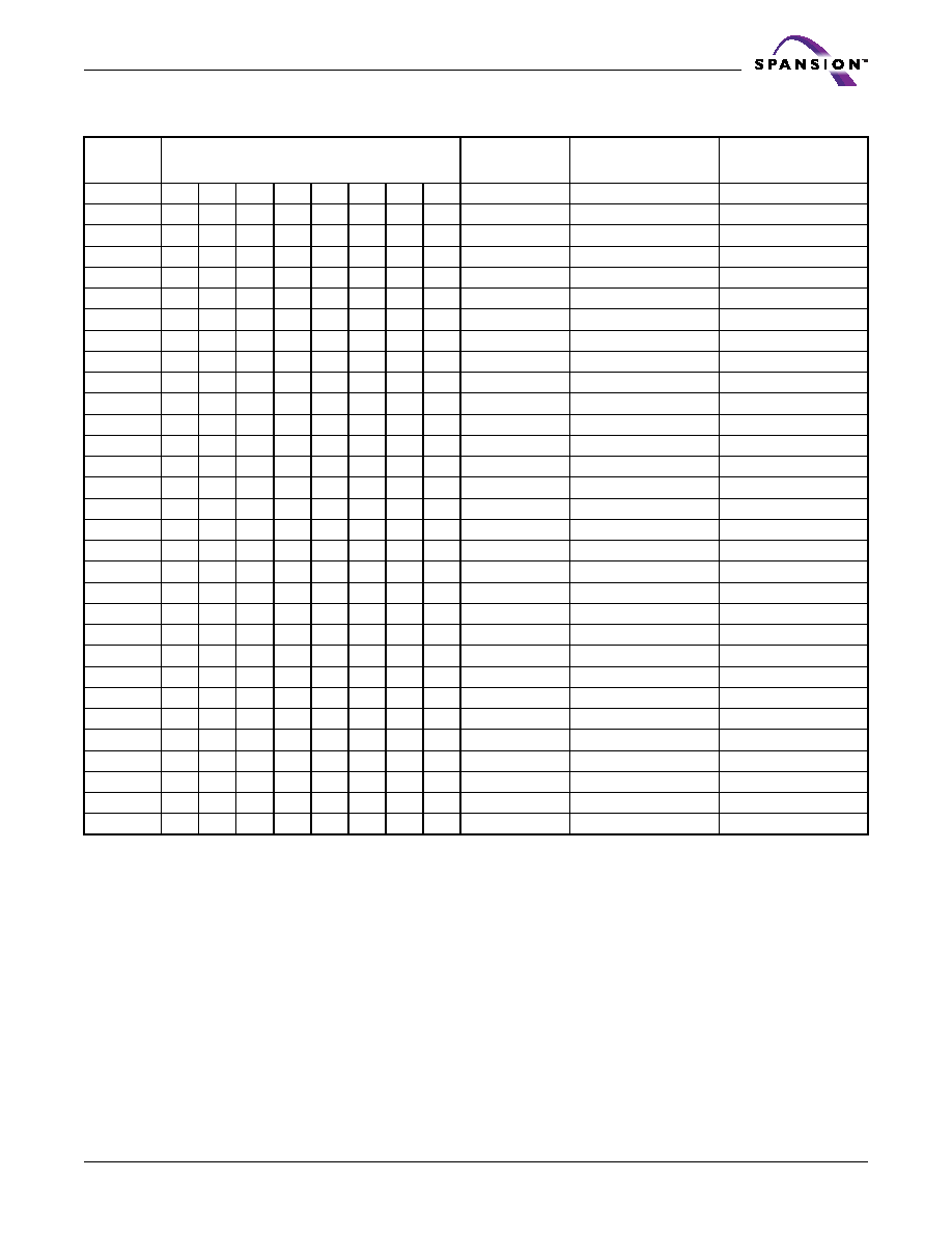
August 4, 2004 S29GLxxxM_00_B1_E
S29GLxxxM MirrorBit
TM
Flash Family
67
D a t a s h e e t
SA225
1
1
1
0
0
0
0
1
64/32
E10000≠E1FFFF
708000≠70FFFF
SA226
1
1
1
0
0
0
1
0
64/32
E20000≠E2FFFF
710000≠717FFF
SA227
1
1
1
0
0
0
1
1
64/32
E30000≠E3FFFF
718000≠71FFFF
SA228
1
1
1
0
0
1
0
0
64/32
E40000≠E4FFFF
720000≠727FFF
SA229
1
1
1
0
0
1
0
1
64/32
E50000≠E5FFFF
728000≠72FFFF
SA230
1
1
1
0
0
1
1
0
64/32
E60000≠E6FFFF
730000≠737FFF
SA231
1
1
1
0
0
1
1
1
64/32
E70000≠E7FFFF
738000≠73FFFF
SA232
1
1
1
0
1
0
0
0
64/32
E80000≠E8FFFF
740000≠747FFF
SA233
1
1
1
0
1
0
0
1
64/32
E90000≠E9FFFF
748000≠74FFFF
SA234
1
1
1
0
1
0
1
0
64/32
EA0000≠EAFFFF
750000≠757FFF
SA235
1
1
1
0
1
0
1
1
64/32
EB0000≠EBFFFF
758000≠75FFFF
SA236
1
1
1
0
1
1
0
0
64/32
EC0000≠ECFFFF
760000≠767FFF
SA237
1
1
1
0
1
1
0
1
64/32
ED0000≠EDFFFF
768000≠76FFFF
SA238
1
1
1
0
1
1
1
0
64/32
EE0000≠EEFFFF
770000≠777FFF
SA239
1
1
1
0
1
1
1
1
64/32
EF0000≠EFFFFF
778000≠77FFFF
SA240
1
1
1
1
0
0
0
0
64/32
F00000≠F0FFFF
780000≠787FFF
SA241
1
1
1
1
0
0
0
1
64/32
F10000≠F1FFFF
788000≠78FFFF
SA242
1
1
1
1
0
0
1
0
64/32
F20000≠F2FFFF
790000≠797FFF
SA243
1
1
1
1
0
0
1
1
64/32
F30000≠F3FFFF
798000≠79FFFF
SA244
1
1
1
1
0
1
0
0
64/32
F40000≠F4FFFF
7A0000≠7A7FFF
SA245
1
1
1
1
0
1
0
1
64/32
F50000≠F5FFFF
7A8000≠7AFFFF
SA246
1
1
1
1
0
1
1
0
64/32
F60000≠F6FFFF
7B0000≠7B7FFF
SA247
1
1
1
1
0
1
1
1
64/32
F70000≠F7FFFF
7B8000≠7BFFFF
SA248
1
1
1
1
1
0
0
0
64/32
F80000≠F8FFFF
7C0000≠7C7FFF
SA249
1
1
1
1
1
0
0
1
64/32
F90000≠F9FFFF
7C8000≠7CFFFF
SA250
1
1
1
1
1
0
1
0
64/32
FA0000≠FAFFFF
7D0000≠7D7FFF
SA251
1
1
1
1
1
0
1
1
64/32
FB0000≠FBFFFF
7D8000≠7DFFFF
SA252
1
1
1
1
1
1
0
0
64/32
FC0000≠FCFFFF
7E0000≠7E7FFF
SA253
1
1
1
1
1
1
0
1
64/32
FD0000≠FDFFFF
7E8000≠7EFFFF
SA254
1
1
1
1
1
1
1
0
64/32
FE0000≠FEFFFF
7F0000≠7F7FFF
SA255
1
1
1
1
1
1
1
1
64/32
FF0000≠FFFFFF
7F8000≠7FFFFF
Table 16. S29GL128M Sector Address Table (Continued)
Sector
A22≠A15
Sector Size
(Kbytes/
Kwords)
8-bit
Address Range
(in hexadecimal)
16-bit
Address Range
(in hexadecimal)

68
S29GLxxxM MirrorBit
TM
Flash Family
S29GLxxxM_00_B1_E August 4, 2004
D a t a s h e e t
Table 17. S29GL256M Sector Address Table
Sector
A23≠A15
Sector Size
(Kbytes/
Kwords)
8-bit
Address Range
(in hexadecimal)
16-bit
Address Range
(in hexadecimal)
SA0
0
0
0
0
0
0
0
0
0
64/32
0000000≠000FFFF
000000≠007FFF
SA1
0
0
0
0
0
0
0
0
1
64/32
0010000≠001FFFF
008000≠00FFFF
SA2
0
0
0
0
0
0
0
1
0
64/32
0020000≠002FFFF
010000≠017FFF
SA3
0
0
0
0
0
0
0
1
1
64/32
0030000≠003FFFF
018000≠01FFFF
SA4
0
0
0
0
0
0
1
0
0
64/32
0040000≠004FFFF
020000≠027FFF
SA5
0
0
0
0
0
0
1
0
1
64/32
0050000≠005FFFF
028000≠02FFFF
SA6
0
0
0
0
0
0
1
1
0
64/32
0060000≠006FFFF
030000≠037FFF
SA7
0
0
0
0
0
0
1
1
1
64/32
0070000≠007FFFF
038000≠03FFFF
SA8
0
0
0
0
0
1
0
0
0
64/32
0080000≠008FFFF
040000≠047FFF
SA9
0
0
0
0
0
1
0
0
1
64/32
0090000≠009FFFF
048000≠04FFFF
SA10
0
0
0
0
0
1
0
1
0
64/32
00A0000≠00AFFFF
050000≠057FFF
SA11
0
0
0
0
0
1
0
1
1
64/32
00B0000≠00BFFFF
058000≠05FFFF
SA12
0
0
0
0
0
1
1
0
0
64/32
00C0000≠00CFFFF
060000≠067FFF
SA13
0
0
0
0
0
1
1
0
1
64/32
00D0000≠00DFFFF
068000≠06FFFF
SA14
0
0
0
0
0
1
1
1
0
64/32
00E0000≠00EFFFF
070000≠077FFF
SA15
0
0
0
0
0
1
1
1
1
64/32
00F0000≠00FFFFF
078000≠07FFFF
SA16
0
0
0
0
1
0
0
0
0
64/32
0100000≠010FFFF
080000≠087FFF
SA17
0
0
0
0
1
0
0
0
1
64/32
0110000≠011FFFF
088000≠08FFFF
SA18
0
0
0
0
1
0
0
1
0
64/32
0120000≠012FFFF
090000≠097FFF
SA19
0
0
0
0
1
0
0
1
1
64/32
0130000≠013FFFF
098000≠09FFFF
SA20
0
0
0
0
1
0
1
0
0
64/32
0140000≠014FFFF
0A0000≠0A7FFF
SA21
0
0
0
0
1
0
1
0
1
64/32
0150000≠015FFFF
0A8000≠0AFFFF
SA22
0
0
0
0
1
0
1
1
0
64/32
0160000≠016FFFF
0B0000≠0B7FFF
SA23
0
0
0
0
1
0
1
1
1
64/32
0170000≠017FFFF
0B8000≠0BFFFF
SA24
0
0
0
0
1
1
0
0
0
64/32
0180000≠018FFFF
0C0000≠0C7FFF
SA25
0
0
0
0
1
1
0
0
1
64/32
0190000≠019FFFF
0C8000≠0CFFFF
SA26
0
0
0
0
1
1
0
1
0
64/32
01A0000≠01AFFFF
0D0000≠0D7FFF
SA27
0
0
0
0
1
1
0
1
1
64/32
01B0000≠01BFFFF
0D8000≠0DFFFF
SA28
0
0
0
0
1
1
1
0
0
64/32
01C0000≠01CFFFF
0E0000≠0E7FFF
SA29
0
0
0
0
1
1
1
0
1
64/32
01D0000≠01DFFFF
0E8000≠0EFFFF
SA30
0
0
0
0
1
1
1
1
0
64/32
01E0000≠01EFFFF
0F0000≠0F7FFF
SA31
0
0
0
0
1
1
1
1
1
64/32
01F0000≠01FFFFF
0F8000≠0FFFFF
SA32
0
0
0
1
0
0
0
0
0
64/32
0200000≠020FFFF
100000≠107FFF
SA33
0
0
0
1
0
0
0
0
1
64/32
0210000≠021FFFF
108000≠10FFFF
SA34
0
0
0
1
0
0
0
1
0
64/32
0220000≠022FFFF
110000≠117FFF
SA35
0
0
0
1
0
0
0
1
1
64/32
0230000≠023FFFF
118000≠11FFFF
SA36
0
0
0
1
0
0
1
0
0
64/32
0240000≠024FFFF
120000≠127FFF
SA37
0
0
0
1
0
0
1
0
1
64/32
0250000≠025FFFF
128000≠12FFFF
SA38
0
0
0
1
0
0
1
1
0
64/32
0260000≠026FFFF
130000≠137FFF
SA39
0
0
0
1
0
0
1
1
1
64/32
0270000≠027FFFF
138000≠13FFFF
SA40
0
0
0
1
0
1
0
0
0
64/32
0280000≠028FFFF
140000≠147FFF
SA41
0
0
0
1
0
1
0
0
1
64/32
0290000≠029FFFF
148000≠14FFFF
SA42
0
0
0
1
0
1
0
1
0
64/32
02A0000≠02AFFFF
150000≠157FFF
SA43
0
0
0
1
0
1
0
1
1
64/32
02B0000≠02BFFFF
158000≠15FFFF
SA44
0
0
0
1
0
1
1
0
0
64/32
02C0000≠02CFFFF
160000≠167FFF

August 4, 2004 S29GLxxxM_00_B1_E
S29GLxxxM MirrorBit
TM
Flash Family
69
D a t a s h e e t
SA45
0
0
0
1
0
1
1
0
1
64/32
02D0000≠02DFFFF
168000≠16FFFF
SA46
0
0
0
1
0
1
1
1
0
64/32
02E0000≠02EFFFF
170000≠177FFF
SA47
0
0
0
1
0
1
1
1
1
64/32
02F0000≠02FFFFF
178000≠17FFFF
SA48
0
0
0
1
1
0
0
0
0
64/32
0300000≠030FFFF
180000≠187FFF
SA49
0
0
0
1
1
0
0
0
1
64/32
0310000≠031FFFF
188000≠18FFFF
SA50
0
0
0
1
1
0
0
1
0
64/32
0320000≠032FFFF
190000≠197FFF
SA51
0
0
0
1
1
0
0
1
1
64/32
0330000≠033FFFF
198000≠19FFFF
SA52
0
0
0
1
1
0
1
0
0
64/32
0340000≠034FFFF
1A0000≠1A7FFF
SA53
0
0
0
1
1
0
1
0
1
64/32
0350000≠035FFFF
1A8000≠1AFFFF
SA54
0
0
0
1
1
0
1
1
0
64/32
0360000≠036FFFF
1B0000≠1B7FFF
SA55
0
0
0
1
1
0
1
1
1
64/32
0370000≠037FFFF
1B8000≠1BFFFF
SA56
0
0
0
1
1
1
0
0
0
64/32
0380000≠038FFFF
1C0000≠1C7FFF
SA57
0
0
0
1
1
1
0
0
1
64/32
0390000≠039FFFF
1C8000≠1CFFFF
SA58
0
0
0
1
1
1
0
1
0
64/32
03A0000≠03AFFFF
1D0000≠1D7FFF
SA59
0
0
0
1
1
1
0
1
1
64/32
03B0000≠03BFFFF
1D8000≠1DFFFF
SA60
0
0
0
1
1
1
1
0
0
64/32
03C0000≠03CFFFF
1E0000≠1E7FFF
SA61
0
0
0
1
1
1
1
0
1
64/32
03D0000≠03DFFFF
1E8000≠1EFFFF
SA62
0
0
0
1
1
1
1
1
0
64/32
03E0000≠03EFFFF
1F0000≠1F7FFF
SA63
0
0
0
1
1
1
1
1
1
64/32
03F0000≠03FFFFF
1F8000≠1FFFFF
SA64
0
0
1
0
0
0
0
0
0
64/32
0400000≠040FFFF
200000≠207FFF
SA65
0
0
1
0
0
0
0
0
1
64/32
0410000≠041FFFF
208000≠20FFFF
SA66
0
0
1
0
0
0
0
1
0
64/32
0420000≠042FFFF
210000≠217FFF
SA67
0
0
1
0
0
0
0
1
1
64/32
0430000≠043FFFF
218000≠21FFFF
SA68
0
0
1
0
0
0
1
0
0
64/32
0440000≠044FFFF
220000≠227FFF
SA69
0
0
1
0
0
0
1
0
1
64/32
0450000≠045FFFF
228000≠22FFFF
SA70
0
0
1
0
0
0
1
1
0
64/32
0460000≠046FFFF
230000≠237FFF
SA71
0
0
1
0
0
0
1
1
1
64/32
0470000≠047FFFF
238000≠23FFFF
SA72
0
0
1
0
0
1
0
0
0
64/32
0480000≠048FFFF
240000≠247FFF
SA73
0
0
1
0
0
1
0
0
1
64/32
0490000≠049FFFF
248000≠24FFFF
SA74
0
0
1
0
0
1
0
1
0
64/32
04A0000≠04AFFFF
250000≠257FFF
SA75
0
0
1
0
0
1
0
1
1
64/32
04B0000≠04BFFFF
258000≠25FFFF
SA76
0
0
1
0
0
1
1
0
0
64/32
04C0000≠04CFFFF
260000≠267FFF
SA77
0
0
1
0
0
1
1
0
1
64/32
04D0000≠04DFFFF
268000≠26FFFF
SA78
0
0
1
0
0
1
1
1
0
64/32
04E0000≠04EFFFF
270000≠277FFF
SA79
0
0
1
0
0
1
1
1
1
64/32
04F0000≠04FFFFF
278000≠27FFFF
SA80
0
0
1
0
1
0
0
0
0
64/32
0500000≠050FFFF
280000≠287FFF
SA81
0
0
1
0
1
0
0
0
1
64/32
0510000≠051FFFF
288000≠28FFFF
SA82
0
0
1
0
1
0
0
1
0
64/32
0520000≠052FFFF
290000≠297FFF
SA83
0
0
1
0
1
0
0
1
1
64/32
0530000≠053FFFF
298000≠29FFFF
SA84
0
0
1
0
1
0
1
0
0
64/32
0540000≠054FFFF
2A0000≠2A7FFF
SA85
0
0
1
0
1
0
1
0
1
64/32
0550000≠055FFFF
2A8000≠2AFFFF
SA86
0
0
1
0
1
0
1
1
0
64/32
0560000≠056FFFF
2B0000≠2B7FFF
SA87
0
0
1
0
1
0
1
1
1
64/32
0570000≠057FFFF
2B8000≠2BFFFF
SA88
0
0
1
0
1
1
0
0
0
64/32
0580000≠058FFFF
2C0000≠2C7FFF
SA89
0
0
1
0
1
1
0
0
1
64/32
0590000≠059FFFF
2C8000≠2CFFFF
Table 17. S29GL256M Sector Address Table (Continued)
Sector
A23≠A15
Sector Size
(Kbytes/
Kwords)
8-bit
Address Range
(in hexadecimal)
16-bit
Address Range
(in hexadecimal)
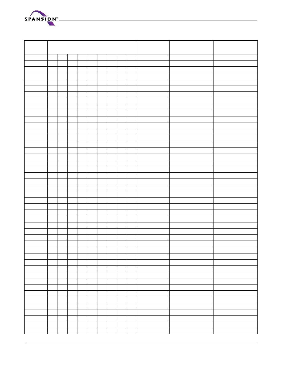
70
S29GLxxxM MirrorBit
TM
Flash Family
S29GLxxxM_00_B1_E August 4, 2004
D a t a s h e e t
SA90
0
0
1
0
1
1
0
1
0
64/32
05A0000≠05AFFFF
2D0000≠2D7FFF
SA91
0
0
1
0
1
1
0
1
1
64/32
05B0000≠05BFFFF
2D8000≠2DFFFF
SA92
0
0
1
0
1
1
1
0
0
64/32
05C0000≠05CFFFF
2E0000≠2E7FFF
SA93
0
0
1
0
1
1
1
0
1
64/32
05D0000≠05DFFFF
2E8000≠2EFFFF
SA94
0
0
1
0
1
1
1
1
0
64/32
05E0000≠05EFFFF
2F0000≠2F7FFF
SA95
0
0
1
0
1
1
1
1
1
64/32
05F0000≠05FFFFF
2F8000≠2FFFFF
SA96
0
0
1
1
0
0
0
0
0
64/32
0600000≠060FFFF
300000≠307FFF
SA97
0
0
1
1
0
0
0
0
1
64/32
0610000≠061FFFF
308000≠30FFFF
SA98
0
0
1
1
0
0
0
1
0
64/32
0620000≠062FFFF
310000≠317FFF
SA99
0
0
1
1
0
0
0
1
1
64/32
0630000≠063FFFF
318000≠31FFFF
SA100
0
0
1
1
0
0
1
0
0
64/32
0640000≠064FFFF
320000≠327FFF
SA101
0
0
1
1
0
0
1
0
1
64/32
0650000≠065FFFF
328000≠32FFFF
SA102
0
0
1
1
0
0
1
1
0
64/32
0660000≠066FFFF
330000≠337FFF
SA103
0
0
1
1
0
0
1
1
1
64/32
0670000≠067FFFF
338000≠33FFFF
SA104
0
0
1
1
0
1
0
0
0
64/32
0680000≠068FFFF
340000≠347FFF
SA105
0
0
1
1
0
1
0
0
1
64/32
0690000≠069FFFF
348000≠34FFFF
SA106
0
0
1
1
0
1
0
1
0
64/32
06A0000≠06AFFFF
350000≠357FFF
SA107
0
0
1
1
0
1
0
1
1
64/32
06B0000≠06BFFFF
358000≠35FFFF
SA108
0
0
1
1
0
1
1
0
0
64/32
06C0000≠06CFFFF
360000≠367FFF
SA109
0
0
1
1
0
1
1
0
1
64/32
06D0000≠06DFFFF
368000≠36FFFF
SA110
0
0
1
1
0
1
1
1
0
64/32
06E0000≠06EFFFF
370000≠377FFF
SA111
0
0
1
1
0
1
1
1
1
64/32
06F0000≠06FFFFF
378000≠37FFFF
SA112
0
0
1
1
1
0
0
0
0
64/32
0700000≠070FFFF
380000≠387FFF
SA113
0
0
1
1
1
0
0
0
1
64/32
0710000≠071FFFF
388000≠38FFFF
SA114
0
0
1
1
1
0
0
1
0
64/32
0720000≠072FFFF
390000≠397FFF
SA115
0
0
1
1
1
0
0
1
1
64/32
0730000≠073FFFF
398000≠39FFFF
SA116
0
0
1
1
1
0
1
0
0
64/32
0740000≠074FFFF
3A0000≠3A7FFF
SA117
0
0
1
1
1
0
1
0
1
64/32
0750000≠075FFFF
3A8000≠3AFFFF
SA118
0
0
1
1
1
0
1
1
0
64/32
0760000≠076FFFF
3B0000≠3B7FFF
SA119
0
0
1
1
1
0
1
1
1
64/32
0770000≠077FFFF
3B8000≠3BFFFF
SA120
0
0
1
1
1
1
0
0
0
64/32
0780000≠078FFFF
3C0000≠3C7FFF
SA121
0
0
1
1
1
1
0
0
1
64/32
0790000≠079FFFF
3C8000≠3CFFFF
SA122
0
0
1
1
1
1
0
1
0
64/32
07A0000≠07AFFFF
3D0000≠3D7FFF
SA123
0
0
1
1
1
1
0
1
1
64/32
07B0000≠07BFFFF
3D8000≠3DFFFF
SA124
0
0
1
1
1
1
1
0
0
64/32
07C0000≠07CFFFF
3E0000≠3E7FFF
SA125
0
0
1
1
1
1
1
0
1
64/32
07D0000≠07DFFFF
3E8000≠3EFFFF
SA126
0
0
1
1
1
1
1
1
0
64/32
07E0000≠07EFFFF
3F0000≠3F7FFF
SA127
0
0
1
1
1
1
1
1
1
64/32
07F0000≠07FFFFF
3F8000≠3FFFFF
SA128
0
1
0
0
0
0
0
0
0
64/32
0800000≠080FFFF
400000≠407FFF
SA129
0
1
0
0
0
0
0
0
1
64/32
0810000≠081FFFF
408000≠40FFFF
SA130
0
1
0
0
0
0
0
1
0
64/32
0820000≠082FFFF
410000≠417FFF
SA131
0
1
0
0
0
0
0
1
1
64/32
0830000≠083FFFF
418000≠41FFFF
SA132
0
1
0
0
0
0
1
0
0
64/32
0840000≠084FFFF
420000≠427FFF
SA133
0
1
0
0
0
0
1
0
1
64/32
0850000≠085FFFF
428000≠42FFFF
SA134
0
1
0
0
0
0
1
1
0
64/32
0860000≠086FFFF
430000≠437FFF
Table 17. S29GL256M Sector Address Table (Continued)
Sector
A23≠A15
Sector Size
(Kbytes/
Kwords)
8-bit
Address Range
(in hexadecimal)
16-bit
Address Range
(in hexadecimal)

August 4, 2004 S29GLxxxM_00_B1_E
S29GLxxxM MirrorBit
TM
Flash Family
71
D a t a s h e e t
SA135
0
1
0
0
0
0
1
1
1
64/32
0870000≠087FFFF
438000≠43FFFF
SA136
0
1
0
0
0
1
0
0
0
64/32
0880000≠088FFFF
440000≠447FFF
SA137
0
1
0
0
0
1
0
0
1
64/32
0890000≠089FFFF
448000≠44FFFF
SA138
0
1
0
0
0
1
0
1
0
64/32
08A0000≠08AFFFF
450000≠457FFF
SA139
0
1
0
0
0
1
0
1
1
64/32
08B0000≠08BFFFF
458000≠45FFFF
SA140
0
1
0
0
0
1
1
0
0
64/32
08C0000≠08CFFFF
460000≠467FFF
SA141
0
1
0
0
0
1
1
0
1
64/32
08D0000≠08DFFFF
468000≠46FFFF
SA142
0
1
0
0
0
1
1
1
0
64/32
08E0000≠08EFFFF
470000≠477FFF
SA143
0
1
0
0
0
1
1
1
1
64/32
08F0000≠08FFFFF
478000≠47FFFF
SA144
0
1
0
0
1
0
0
0
0
64/32
0900000≠090FFFF
480000≠487FFF
SA145
0
1
0
0
1
0
0
0
1
64/32
0910000≠091FFFF
488000≠48FFFF
SA146
0
1
0
0
1
0
0
1
0
64/32
0920000≠092FFFF
490000≠497FFF
SA147
0
1
0
0
1
0
0
1
1
64/32
0930000≠093FFFF
498000≠49FFFF
SA148
0
1
0
0
1
0
1
0
0
64/32
0940000≠094FFFF
4A0000≠4A7FFF
SA149
0
1
0
0
1
0
1
0
1
64/32
0950000≠095FFFF
4A8000≠4AFFFF
SA150
0
1
0
0
1
0
1
1
0
64/32
0960000≠096FFFF
4B0000≠4B7FFF
SA151
0
1
0
0
1
0
1
1
1
64/32
0970000≠097FFFF
4B8000≠4BFFFF
SA152
0
1
0
0
1
1
0
0
0
64/32
0980000≠098FFFF
4C0000≠4C7FFF
SA153
0
1
0
0
1
1
0
0
1
64/32
0990000≠099FFFF
4C8000≠4CFFFF
SA154
0
1
0
0
1
1
0
1
0
64/32
09A0000≠09AFFFF
4D0000≠4D7FFF
SA155
0
1
0
0
1
1
0
1
1
64/32
09B0000≠09BFFFF
4D8000≠4DFFFF
SA156
0
1
0
0
1
1
1
0
0
64/32
09C0000≠09CFFFF
4E0000≠4E7FFF
SA157
0
1
0
0
1
1
1
0
1
64/32
09D0000≠09DFFFF
4E8000≠4EFFFF
SA158
0
1
0
0
1
1
1
1
0
64/32
09E0000≠09EFFFF
4F0000≠4F7FFF
SA159
0
1
0
0
1
1
1
1
1
64/32
09F0000≠09FFFFF
4F8000≠4FFFFF
SA160
0
1
0
1
0
0
0
0
0
64/32
0A00000≠0A0FFFF
500000≠507FFF
SA161
0
1
0
1
0
0
0
0
1
64/32
0A10000≠0A1FFFF
508000≠50FFFF
SA162
0
1
0
1
0
0
0
1
0
64/32
0A20000≠0A2FFFF
510000≠517FFF
SA163
0
1
0
1
0
0
0
1
1
64/32
0A30000≠0A3FFFF
518000≠51FFFF
SA164
0
1
0
1
0
0
1
0
0
64/32
0A40000≠0A4FFFF
520000≠527FFF
SA165
0
1
0
1
0
0
1
0
1
64/32
0A50000≠0A5FFFF
528000≠52FFFF
SA166
0
1
0
1
0
0
1
1
0
64/32
0A60000≠0A6FFFF
530000≠537FFF
SA167
0
1
0
1
0
0
1
1
1
64/32
0A70000≠0A7FFFF
538000≠53FFFF
SA168
0
1
0
1
0
1
0
0
0
64/32
0A80000≠0A8FFFF
540000≠547FFF
SA169
0
1
0
1
0
1
0
0
1
64/32
0A90000≠0A9FFFF
548000≠54FFFF
SA170
0
1
0
1
0
1
0
1
0
64/32
0AA0000≠0AAFFFF
550000≠557FFF
SA171
0
1
0
1
0
1
0
1
1
64/32
0AB0000≠0ABFFFF
558000≠55FFFF
SA172
0
1
0
1
0
1
1
0
0
64/32
0AC0000≠0ACFFFF
560000≠567FFF
SA173
0
1
0
1
0
1
1
0
1
64/32
0AD0000≠0ADFFFF
568000≠56FFFF
SA174
0
1
0
1
0
1
1
1
0
64/32
0AE0000≠0AEFFFF
570000≠577FFF
SA175
0
1
0
1
0
1
1
1
1
64/32
0AF0000≠0AFFFFF
578000≠57FFFF
SA176
0
1
0
1
1
0
0
0
0
64/32
0B00000≠0B0FFFF
580000≠587FFF
SA177
0
1
0
1
1
0
0
0
1
64/32
0B10000≠0B1FFFF
588000≠58FFFF
SA178
0
1
0
1
1
0
0
1
0
64/32
0B20000≠0B2FFFF
590000≠597FFF
SA179
0
1
0
1
1
0
0
1
1
64/32
0B30000≠0B3FFFF
598000≠59FFFF
Table 17. S29GL256M Sector Address Table (Continued)
Sector
A23≠A15
Sector Size
(Kbytes/
Kwords)
8-bit
Address Range
(in hexadecimal)
16-bit
Address Range
(in hexadecimal)

72
S29GLxxxM MirrorBit
TM
Flash Family
S29GLxxxM_00_B1_E August 4, 2004
D a t a s h e e t
SA180
0
1
0
1
1
0
1
0
0
64/32
0B40000≠0B4FFFF
5A0000≠5A7FFF
SA181
0
1
0
1
1
0
1
0
1
64/32
0B50000≠0B5FFFF
5A8000≠5AFFFF
SA182
0
1
0
1
1
0
1
1
0
64/32
0B60000≠0B6FFFF
5B0000≠5B7FFF
SA183
0
1
0
1
1
0
1
1
1
64/32
0B70000≠0B7FFFF
5B8000≠5BFFFF
SA184
0
1
0
1
1
1
0
0
0
64/32
0B80000≠0B8FFFF
5C0000≠5C7FFF
SA185
0
1
0
1
1
1
0
0
1
64/32
0B90000≠0B9FFFF
5C8000≠5CFFFF
SA186
0
1
0
1
1
1
0
1
0
64/32
0BA0000≠0BAFFFF
5D0000≠5D7FFF
SA187
0
1
0
1
1
1
0
1
1
64/32
0BB0000≠0BBFFFF
5D8000≠5DFFFF
SA188
0
1
0
1
1
1
1
0
0
64/32
0BC0000≠0BCFFFF
5E0000≠5E7FFF
SA189
0
1
0
1
1
1
1
0
1
64/32
0BD0000≠0BDFFFF
5E8000≠5EFFFF
SA190
0
1
0
1
1
1
1
1
0
64/32
0BE0000≠0BEFFFF
5F0000≠5F7FFF
SA191
0
1
0
1
1
1
1
1
1
64/32
0BF0000≠0BFFFFF
5F8000≠5FFFFF
SA192
0
1
1
0
0
0
0
0
0
64/32
0C00000≠0C0FFFF
600000≠607FFF
SA193
0
1
1
0
0
0
0
0
1
64/32
0C10000≠0C1FFFF
608000≠60FFFF
SA194
0
1
1
0
0
0
0
1
0
64/32
0C20000≠0C2FFFF
610000≠617FFF
SA195
0
1
1
0
0
0
0
1
1
64/32
0C30000≠0C3FFFF
618000≠61FFFF
SA196
0
1
1
0
0
0
1
0
0
64/32
0C40000≠0C4FFFF
620000≠627FFF
SA197
0
1
1
0
0
0
1
0
1
64/32
0C50000≠0C5FFFF
628000≠62FFFF
SA198
0
1
1
0
0
0
1
1
0
64/32
0C60000≠0C6FFFF
630000≠637FFF
SA199
0
1
1
0
0
0
1
1
1
64/32
0C70000≠0C7FFFF
638000≠63FFFF
SA200
0
1
1
0
0
1
0
0
0
64/32
0C80000≠0C8FFFF
640000≠647FFF
SA201
0
1
1
0
0
1
0
0
1
64/32
0C90000≠0C9FFFF
648000≠64FFFF
SA202
0
1
1
0
0
1
0
1
0
64/32
0CA0000≠0CAFFFF
650000≠657FFF
SA203
0
1
1
0
0
1
0
1
1
64/32
0CB0000≠0CBFFFF
658000≠65FFFF
SA204
0
1
1
0
0
1
1
0
0
64/32
0CC0000≠0CCFFFF
660000≠667FFF
SA205
0
1
1
0
0
1
1
0
1
64/32
0CD0000≠0CDFFFF
668000≠66FFFF
SA206
0
1
1
0
0
1
1
1
0
64/32
0CE0000≠0CEFFFF
670000≠677FFF
SA207
0
1
1
0
0
1
1
1
1
64/32
0CF0000≠0CFFFFF
678000≠67FFFF
SA208
0
1
1
0
1
0
0
0
0
64/32
0D00000≠0D0FFFF
680000≠687FFF
SA209
0
1
1
0
1
0
0
0
1
64/32
0D10000≠0D1FFFF
688000≠68FFFF
SA210
0
1
1
0
1
0
0
1
0
64/32
0D20000≠0D2FFFF
690000≠697FFF
SA211
0
1
1
0
1
0
0
1
1
64/32
0D30000≠0D3FFFF
698000≠69FFFF
SA212
0
1
1
0
1
0
1
0
0
64/32
0D40000≠0D4FFFF
6A0000≠6A7FFF
SA213
0
1
1
0
1
0
1
0
1
64/32
0D50000≠0D5FFFF
6A8000≠6AFFFF
SA214
0
1
1
0
1
0
1
1
0
64/32
0D60000≠0D6FFFF
6B0000≠6B7FFF
SA215
0
1
1
0
1
0
1
1
1
64/32
0D70000≠0D7FFFF
6B8000≠6BFFFF
SA216
0
1
1
0
1
1
0
0
0
64/32
0D80000≠0D8FFFF
6C0000≠6C7FFF
SA217
0
1
1
0
1
1
0
0
1
64/32
0D90000≠0D9FFFF
6C8000≠6CFFFF
SA218
0
1
1
0
1
1
0
1
0
64/32
0DA0000≠0DAFFFF
6D0000≠6D7FFF
SA219
0
1
1
0
1
1
0
1
1
64/32
0DB0000≠0DBFFFF
6D8000≠6DFFFF
SA220
0
1
1
0
1
1
1
0
0
64/32
0DC0000≠0DCFFFF
6E0000≠6E7FFF
SA221
0
1
1
0
1
1
1
0
1
64/32
0DD0000≠0DDFFFF
6E8000≠6EFFFF
SA222
0
1
1
0
1
1
1
1
0
64/32
0DE0000≠0DEFFFF
6F0000≠6F7FFF
SA223
0
1
1
0
1
1
1
1
1
64/32
0DF0000≠0DFFFFF
6F8000≠6FFFFF
SA224
0
1
1
1
0
0
0
0
0
64/32
0E00000≠0E0FFFF
700000≠707FFF
Table 17. S29GL256M Sector Address Table (Continued)
Sector
A23≠A15
Sector Size
(Kbytes/
Kwords)
8-bit
Address Range
(in hexadecimal)
16-bit
Address Range
(in hexadecimal)

August 4, 2004 S29GLxxxM_00_B1_E
S29GLxxxM MirrorBit
TM
Flash Family
73
D a t a s h e e t
SA225
0
1
1
1
0
0
0
0
1
64/32
0E10000≠0E1FFFF
708000≠70FFFF
SA226
0
1
1
1
0
0
0
1
0
64/32
0E20000≠0E2FFFF
710000≠717FFF
SA227
0
1
1
1
0
0
0
1
1
64/32
0E30000≠0E3FFFF
718000≠71FFFF
SA228
0
1
1
1
0
0
1
0
0
64/32
0E40000≠0E4FFFF
720000≠727FFF
SA229
0
1
1
1
0
0
1
0
1
64/32
0E50000≠0E5FFFF
728000≠72FFFF
SA230
0
1
1
1
0
0
1
1
0
64/32
0E60000≠0E6FFFF
730000≠737FFF
SA231
0
1
1
1
0
0
1
1
1
64/32
0E70000≠0E7FFFF
738000≠73FFFF
SA232
0
1
1
1
0
1
0
0
0
64/32
0E80000≠0E8FFFF
740000≠747FFF
SA233
0
1
1
1
0
1
0
0
1
64/32
0E90000≠0E9FFFF
748000≠74FFFF
SA234
0
1
1
1
0
1
0
1
0
64/32
0EA0000≠0EAFFFF
750000≠757FFF
SA235
0
1
1
1
0
1
0
1
1
64/32
0EB0000≠0EBFFFF
758000≠75FFFF
SA236
0
1
1
1
0
1
1
0
0
64/32
0EC0000≠0ECFFFF
760000≠767FFF
SA237
0
1
1
1
0
1
1
0
1
64/32
0ED0000≠0EDFFFF
768000≠76FFFF
SA238
0
1
1
1
0
1
1
1
0
64/32
0EE0000≠0EEFFFF
770000≠777FFF
SA239
0
1
1
1
0
1
1
1
1
64/32
0EF0000≠0EFFFFF
778000≠77FFFF
SA240
0
1
1
1
1
0
0
0
0
64/32
0F00000≠0F0FFFF
780000≠787FFF
SA241
0
1
1
1
1
0
0
0
1
64/32
0F10000≠0F1FFFF
788000≠78FFFF
SA242
0
1
1
1
1
0
0
1
0
64/32
0F20000≠0F2FFFF
790000≠797FFF
SA243
0
1
1
1
1
0
0
1
1
64/32
0F30000≠0F3FFFF
798000≠79FFFF
SA244
0
1
1
1
1
0
1
0
0
64/32
0F40000≠0F4FFFF
7A0000≠7A7FFF
SA245
0
1
1
1
1
0
1
0
1
64/32
0F50000≠0F5FFFF
7A8000≠7AFFFF
SA246
0
1
1
1
1
0
1
1
0
64/32
0F60000≠0F6FFFF
7B0000≠7B7FFF
SA247
0
1
1
1
1
0
1
1
1
64/32
0F70000≠0F7FFFF
7B8000≠7BFFFF
SA248
0
1
1
1
1
1
0
0
0
64/32
0F80000≠0F8FFFF
7C0000≠7C7FFF
SA249
0
1
1
1
1
1
0
0
1
64/32
0F90000≠0F9FFFF
7C8000≠7CFFFF
SA250
0
1
1
1
1
1
0
1
0
64/32
0FA0000≠0FAFFFF
7D0000≠7D7FFF
SA251
0
1
1
1
1
1
0
1
1
64/32
0FB0000≠0FBFFFF
7D8000≠7DFFFF
SA252
0
1
1
1
1
1
1
0
0
64/32
0FC0000≠0FCFFFF
7E0000≠7E7FFF
SA253
0
1
1
1
1
1
1
0
1
64/32
0FD0000≠0FDFFFF
7E8000≠7EFFFF
SA254
0
1
1
1
1
1
1
1
0
64/32
0FE0000≠0FEFFFF
7F0000≠7F7FFF
SA255
0
1
1
1
1
1
1
1
1
64/32
0FF0000≠0FFFFFF
7F8000≠7FFFFF
SA256
1
0
0
0
0
0
0
0
0
64/32
1000000≠100FFFF
800000≠807FFF
SA257
1
0
0
0
0
0
0
0
1
64/32
1010000≠101FFFF
808000≠80FFFF
SA258
1
0
0
0
0
0
0
1
0
64/32
1020000≠102FFFF
810000≠817FFF
SA259
1
0
0
0
0
0
0
1
1
64/32
1030000≠103FFFF
818000≠81FFFF
SA260
1
0
0
0
0
0
1
0
0
64/32
1040000≠104FFFF
820000≠827FFF
SA261
1
0
0
0
0
0
1
0
1
64/32
1050000≠105FFFF
828000≠82FFFF
SA262
1
0
0
0
0
0
1
1
0
64/32
1060000≠106FFFF
830000≠837FFF
SA263
1
0
0
0
0
0
1
1
1
64/32
1070000≠107FFFF
838000≠83FFFF
SA264
1
0
0
0
0
1
0
0
0
64/32
1080000≠108FFFF
840000≠847FFF
SA265
1
0
0
0
0
1
0
0
1
64/32
1090000≠109FFFF
848000≠84FFFF
SA266
1
0
0
0
0
1
0
1
0
64/32
10A0000≠10AFFFF
850000≠857FFF
SA267
1
0
0
0
0
1
0
1
1
64/32
10B0000≠10BFFFF
858000≠85FFFF
SA268
1
0
0
0
0
1
1
0
0
64/32
10C0000≠10CFFFF
860000≠867FFF
SA269
1
0
0
0
0
1
1
0
1
64/32
10D0000≠10DFFFF
868000≠86FFFF
Table 17. S29GL256M Sector Address Table (Continued)
Sector
A23≠A15
Sector Size
(Kbytes/
Kwords)
8-bit
Address Range
(in hexadecimal)
16-bit
Address Range
(in hexadecimal)
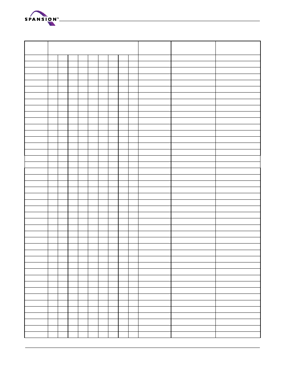
74
S29GLxxxM MirrorBit
TM
Flash Family
S29GLxxxM_00_B1_E August 4, 2004
D a t a s h e e t
SA270
1
0
0
0
0
1
1
1
0
64/32
10E0000≠10EFFFF
870000≠877FFF
SA271
1
0
0
0
0
1
1
1
1
64/32
10F0000≠10FFFFF
878000≠87FFFF
SA272
1
0
0
0
1
0
0
0
0
64/32
1100000≠110FFFF
880000≠887FFF
SA273
1
0
0
0
1
0
0
0
1
64/32
1110000≠111FFFF
888000≠88FFFF
SA274
1
0
0
0
1
0
0
1
0
64/32
1120000≠112FFFF
890000≠897FFF
SA275
1
0
0
0
1
0
0
1
1
64/32
1130000≠113FFFF
898000≠89FFFF
SA276
1
0
0
0
1
0
1
0
0
64/32
1140000≠114FFFF
8A0000≠8A7FFF
SA277
1
0
0
0
1
0
1
0
1
64/32
1150000≠115FFFF
8A8000≠8AFFFF
SA278
1
0
0
0
1
0
1
1
0
64/32
1160000≠116FFFF
8B0000≠8B7FFF
SA279
1
0
0
0
1
0
1
1
1
64/32
1170000≠117FFFF
8B8000≠8BFFFF
SA280
1
0
0
0
1
1
0
0
0
64/32
1180000≠118FFFF
8C0000≠8C7FFF
SA281
1
0
0
0
1
1
0
0
1
64/32
1190000≠119FFFF
8C8000≠8CFFFF
SA282
1
0
0
0
1
1
0
1
0
64/32
11A0000≠11AFFFF
8D0000≠8D7FFF
SA283
1
0
0
0
1
1
0
1
1
64/32
11B0000≠11BFFFF
8D8000≠8DFFFF
SA284
1
0
0
0
1
1
1
0
0
64/32
11C0000≠11CFFFF
8E0000≠8E7FFF
SA285
1
0
0
0
1
1
1
0
1
64/32
11D0000≠11DFFFF
8E8000≠8EFFFF
SA286
1
0
0
0
1
1
1
1
0
64/32
11E0000≠11EFFFF
8F0000≠8F7FFF
SA287
1
0
0
0
1
1
1
1
1
64/32
11F0000≠11FFFFF
8F8000≠8FFFFF
SA288
1
0
0
1
0
0
0
0
0
64/32
1200000≠120FFFF
900000≠907FFF
SA289
1
0
0
1
0
0
0
0
1
64/32
1210000≠121FFFF
908000≠90FFFF
SA290
1
0
0
1
0
0
0
1
0
64/32
1220000≠122FFFF
910000≠917FFF
SA291
1
0
0
1
0
0
0
1
1
64/32
1230000≠123FFFF
918000≠91FFFF
SA292
1
0
0
1
0
0
1
0
0
64/32
1240000≠124FFFF
920000≠927FFF
SA293
1
0
0
1
0
0
1
0
1
64/32
1250000≠125FFFF
928000≠92FFFF
SA294
1
0
0
1
0
0
1
1
0
64/32
1260000≠126FFFF
930000≠937FFF
SA295
1
0
0
1
0
0
1
1
1
64/32
1270000≠127FFFF
938000≠93FFFF
SA296
1
0
0
1
0
1
0
0
0
64/32
1280000≠128FFFF
940000≠947FFF
SA297
1
0
0
1
0
1
0
0
1
64/32
1290000≠129FFFF
948000≠94FFFF
SA298
1
0
0
1
0
1
0
1
0
64/32
12A0000≠12AFFFF
950000≠957FFF
SA299
1
0
0
1
0
1
0
1
1
64/32
12B0000≠12BFFFF
958000≠95FFFF
SA300
1
0
0
1
0
1
1
0
0
64/32
12C0000≠12CFFFF
960000≠967FFF
SA301
1
0
0
1
0
1
1
0
1
64/32
12D0000≠12DFFFF
968000≠96FFFF
SA302
1
0
0
1
0
1
1
1
0
64/32
12E0000≠12EFFFF
970000≠977FFF
SA303
1
0
0
1
0
1
1
1
1
64/32
12F0000≠12FFFFF
978000≠97FFFF
SA304
1
0
0
1
1
0
0
0
0
64/32
1300000≠130FFFF
980000≠987FFF
SA305
1
0
0
1
1
0
0
0
1
64/32
1310000≠131FFFF
988000≠98FFFF
SA306
1
0
0
1
1
0
0
1
0
64/32
1320000≠132FFFF
990000≠997FFF
SA307
1
0
0
1
1
0
0
1
1
64/32
1330000≠133FFFF
998000≠99FFFF
SA308
1
0
0
1
1
0
1
0
0
64/32
1340000≠134FFFF
9A0000≠9A7FFF
SA309
1
0
0
1
1
0
1
0
1
64/32
1350000≠135FFFF
9A8000≠9AFFFF
SA310
1
0
0
1
1
0
1
1
0
64/32
1360000≠136FFFF
9B0000≠9B7FFF
SA311
1
0
0
1
1
0
1
1
1
64/32
1370000≠137FFFF
9B8000≠9BFFFF
SA312
1
0
0
1
1
1
0
0
0
64/32
1380000≠138FFFF
9C0000≠9C7FFF
SA313
1
0
0
1
1
1
0
0
1
64/32
1390000≠139FFFF
9C8000≠9CFFFF
SA314
1
0
0
1
1
1
0
1
0
64/32
13A0000≠13AFFFF
9D0000≠9D7FFF
Table 17. S29GL256M Sector Address Table (Continued)
Sector
A23≠A15
Sector Size
(Kbytes/
Kwords)
8-bit
Address Range
(in hexadecimal)
16-bit
Address Range
(in hexadecimal)

August 4, 2004 S29GLxxxM_00_B1_E
S29GLxxxM MirrorBit
TM
Flash Family
75
D a t a s h e e t
SA315
1
0
0
1
1
1
0
1
1
64/32
13B0000≠13BFFFF
9D8000≠9DFFFF
SA316
1
0
0
1
1
1
1
0
0
64/32
13C0000≠13CFFFF
9E0000≠9E7FFF
SA317
1
0
0
1
1
1
1
0
1
64/32
13D0000≠13DFFFF
9E8000≠9EFFFF
SA318
1
0
0
1
1
1
1
1
0
64/32
13E0000≠13EFFFF
9F0000≠9F7FFF
SA319
1
0
0
1
1
1
1
1
1
64/32
13F0000≠13FFFFF
9F8000≠9FFFFF
SA320
1
0
1
0
0
0
0
0
0
64/32
1400000≠140FFFF
A00000≠A07FFF
SA321
1
0
1
0
0
0
0
0
1
64/32
1410000≠141FFFF
A08000≠A0FFFF
SA322
1
0
1
0
0
0
0
1
0
64/32
1420000≠142FFFF
A10000≠A17FFF
SA323
1
0
1
0
0
0
0
1
1
64/32
1430000≠143FFFF
A18000≠A1FFFF
SA324
1
0
1
0
0
0
1
0
0
64/32
1440000≠144FFFF
A20000≠A27FFF
SA325
1
0
1
0
0
0
1
0
1
64/32
1450000≠145FFFF
A28000≠A2FFFF
SA326
1
0
1
0
0
0
1
1
0
64/32
1460000≠146FFFF
A30000≠A37FFF
SA327
1
0
1
0
0
0
1
1
1
64/32
1470000≠147FFFF
A38000≠A3FFFF
SA328
1
0
1
0
0
1
0
0
0
64/32
1480000≠148FFFF
A40000≠A47FFF
SA329
1
0
1
0
0
1
0
0
1
64/32
1490000≠149FFFF
A48000≠A4FFFF
SA330
1
0
1
0
0
1
0
1
0
64/32
14A0000≠14AFFFF
A50000≠A57FFF
SA331
1
0
1
0
0
1
0
1
1
64/32
14B0000≠14BFFFF
A58000≠A5FFFF
SA332
1
0
1
0
0
1
1
0
0
64/32
14C0000≠14CFFFF
A60000≠A67FFF
SA333
1
0
1
0
0
1
1
0
1
64/32
14D0000≠14DFFFF
A68000≠A6FFFF
SA334
1
0
1
0
0
1
1
1
0
64/32
14E0000≠14EFFFF
A70000≠A77FFF
SA335
1
0
1
0
0
1
1
1
1
64/32
14F0000≠14FFFFF
A78000≠A7FFFF
SA336
1
0
1
0
1
0
0
0
0
64/32
1500000≠150FFFF
A80000≠A87FFF
SA337
1
0
1
0
1
0
0
0
1
64/32
1510000≠151FFFF
A88000≠A8FFFF
SA338
1
0
1
0
1
0
0
1
0
64/32
1520000≠152FFFF
A90000≠A97FFF
SA339
1
0
1
0
1
0
0
1
1
64/32
1530000≠153FFFF
A98000≠A9FFFF
SA340
1
0
1
0
1
0
1
0
0
64/32
1540000≠154FFFF
AA0000≠AA7FFF
SA341
1
0
1
0
1
0
1
0
1
64/32
1550000≠155FFFF
AA8000≠AAFFFF
SA342
1
0
1
0
1
0
1
1
0
64/32
1560000≠156FFFF
AB0000≠AB7FFF
SA343
1
0
1
0
1
0
1
1
1
64/32
1570000≠157FFFF
AB8000≠ABFFFF
SA344
1
0
1
0
1
1
0
0
0
64/32
1580000≠158FFFF
AC0000≠AC7FFF
SA345
1
0
1
0
1
1
0
0
1
64/32
1590000≠159FFFF
AC8000≠ACFFFF
SA346
1
0
1
0
1
1
0
1
0
64/32
15A0000≠15AFFFF
AD0000≠AD7FFF
SA347
1
0
1
0
1
1
0
1
1
64/32
15B0000≠15BFFFF
AD8000≠ADFFFF
SA348
1
0
1
0
1
1
1
0
0
64/32
15C0000≠15CFFFF
AE0000≠AE7FFF
SA349
1
0
1
0
1
1
1
0
1
64/32
15D0000≠15DFFFF
AE8000≠AEFFFF
SA350
1
0
1
0
1
1
1
1
0
64/32
15E0000≠15EFFFF
AF0000≠AF7FFF
SA351
1
0
1
0
1
1
1
1
1
64/32
15F0000≠15FFFFF
AF8000≠AFFFFF
SA352
1
0
1
1
0
0
0
0
0
64/32
1600000≠160FFFF
B00000≠B07FFF
SA353
1
0
1
1
0
0
0
0
1
64/32
1610000≠161FFFF
B08000≠B0FFFF
SA354
1
0
1
1
0
0
0
1
0
64/32
1620000≠162FFFF
B10000≠B17FFF
SA355
1
0
1
1
0
0
0
1
1
64/32
1630000≠163FFFF
B18000≠B1FFFF
SA356
1
0
1
1
0
0
1
0
0
64/32
1640000≠164FFFF
B20000≠B27FFF
SA357
1
0
1
1
0
0
1
0
1
64/32
1650000≠165FFFF
B28000≠B2FFFF
SA358
1
0
1
1
0
0
1
1
0
64/32
1660000≠166FFFF
B30000≠B37FFF
SA359
1
0
1
1
0
0
1
1
1
64/32
1670000≠167FFFF
B38000≠B3FFFF
Table 17. S29GL256M Sector Address Table (Continued)
Sector
A23≠A15
Sector Size
(Kbytes/
Kwords)
8-bit
Address Range
(in hexadecimal)
16-bit
Address Range
(in hexadecimal)

76
S29GLxxxM MirrorBit
TM
Flash Family
S29GLxxxM_00_B1_E August 4, 2004
D a t a s h e e t
SA360
1
0
1
1
0
1
0
0
0
64/32
1680000≠168FFFF
B40000≠B47FFF
SA361
1
0
1
1
0
1
0
0
1
64/32
1690000≠169FFFF
B48000≠B4FFFF
SA362
1
0
1
1
0
1
0
1
0
64/32
16A0000≠16AFFFF
B50000≠B57FFF
SA363
1
0
1
1
0
1
0
1
1
64/32
16B0000≠16BFFFF
B58000≠B5FFFF
SA364
1
0
1
1
0
1
1
0
0
64/32
16C0000≠16CFFFF
B60000≠B67FFF
SA365
1
0
1
1
0
1
1
0
1
64/32
16D0000≠16DFFFF
B68000≠B6FFFF
SA366
1
0
1
1
0
1
1
1
0
64/32
16E0000≠16EFFFF
B70000≠B77FFF
SA367
1
0
1
1
0
1
1
1
1
64/32
16F0000≠16FFFFF
B78000≠B7FFFF
SA368
1
0
1
1
1
0
0
0
0
64/32
1700000≠170FFFF
B80000≠B87FFF
SA369
1
0
1
1
1
0
0
0
1
64/32
1710000≠171FFFF
B88000≠B8FFFF
SA370
1
0
1
1
1
0
0
1
0
64/32
1720000≠172FFFF
B90000≠B97FFF
SA371
1
0
1
1
1
0
0
1
1
64/32
1730000≠173FFFF
B98000≠B9FFFF
SA372
1
0
1
1
1
0
1
0
0
64/32
1740000≠174FFFF
BA0000≠BA7FFF
SA373
1
0
1
1
1
0
1
0
1
64/32
1750000≠175FFFF
BA8000≠BAFFFF
SA374
1
0
1
1
1
0
1
1
0
64/32
1760000≠176FFFF
BB0000≠BB7FFF
SA375
1
0
1
1
1
0
1
1
1
64/32
1770000≠177FFFF
BB8000≠BBFFFF
SA376
1
0
1
1
1
1
0
0
0
64/32
1780000≠178FFFF
BC0000≠BC7FFF
SA377
1
0
1
1
1
1
0
0
1
64/32
1790000≠179FFFF
BC8000≠BCFFFF
SA378
1
0
1
1
1
1
0
1
0
64/32
17A0000≠17AFFFF
BD0000≠BD7FFF
SA379
1
0
1
1
1
1
0
1
1
64/32
17B0000≠17BFFFF
BD8000≠BDFFFF
SA380
1
0
1
1
1
1
1
0
0
64/32
17C0000≠17CFFFF
BE0000≠BE7FFF
SA381
1
0
1
1
1
1
1
0
1
64/32
17D0000≠17DFFFF
BE8000≠BEFFFF
SA382
1
0
1
1
1
1
1
1
0
64/32
17E0000≠17EFFFF
BF0000≠BF7FFF
SA383
1
0
1
1
1
1
1
1
1
64/32
17F0000≠17FFFFF
BF8000≠BFFFFF
SA384
1
1
0
0
0
0
0
0
0
64/32
1800000≠180FFFF
C00000≠C07FFF
SA385
1
1
0
0
0
0
0
0
1
64/32
1810000≠181FFFF
C08000≠C0FFFF
SA386
1
1
0
0
0
0
0
1
0
64/32
1820000≠182FFFF
C10000≠C17FFF
SA387
1
1
0
0
0
0
0
1
1
64/32
1830000≠183FFFF
C18000≠C1FFFF
SA388
1
1
0
0
0
0
1
0
0
64/32
1840000≠184FFFF
C20000≠C27FFF
SA389
1
1
0
0
0
0
1
0
1
64/32
1850000≠185FFFF
C28000≠C2FFFF
SA390
1
1
0
0
0
0
1
1
0
64/32
1860000≠186FFFF
C30000≠C37FFF
SA391
1
1
0
0
0
0
1
1
1
64/32
1870000≠187FFFF
C38000≠C3FFFF
SA392
1
1
0
0
0
1
0
0
0
64/32
1880000≠188FFFF
C40000≠C47FFF
SA393
1
1
0
0
0
1
0
0
1
64/32
1890000≠189FFFF
C48000≠C4FFFF
SA394
1
1
0
0
0
1
0
1
0
64/32
18A0000≠18AFFFF
C50000≠C57FFF
SA395
1
1
0
0
0
1
0
1
1
64/32
18B0000≠18BFFFF
C58000≠C5FFFF
SA396
1
1
0
0
0
1
1
0
0
64/32
18C0000≠18CFFFF
C60000≠C67FFF
SA397
1
1
0
0
0
1
1
0
1
64/32
18D0000≠18DFFFF
C68000≠C6FFFF
SA398
1
1
0
0
0
1
1
1
0
64/32
18E0000≠18EFFFF
C70000≠C77FFF
SA399
1
1
0
0
0
1
1
1
1
64/32
18F0000≠18FFFFF
C78000≠C7FFFF
SA400
1
1
0
0
1
0
0
0
0
64/32
1900000≠190FFFF
C80000≠C87FFF
SA401
1
1
0
0
1
0
0
0
1
64/32
1910000≠191FFFF
C88000≠C8FFFF
SA402
1
1
0
0
1
0
0
1
0
64/32
1920000≠192FFFF
C90000≠C97FFF
SA403
1
1
0
0
1
0
0
1
1
64/32
1930000≠193FFFF
C98000≠C9FFFF
SA404
1
1
0
0
1
0
1
0
0
64/32
1940000≠194FFFF
CA0000≠CA7FFF
Table 17. S29GL256M Sector Address Table (Continued)
Sector
A23≠A15
Sector Size
(Kbytes/
Kwords)
8-bit
Address Range
(in hexadecimal)
16-bit
Address Range
(in hexadecimal)
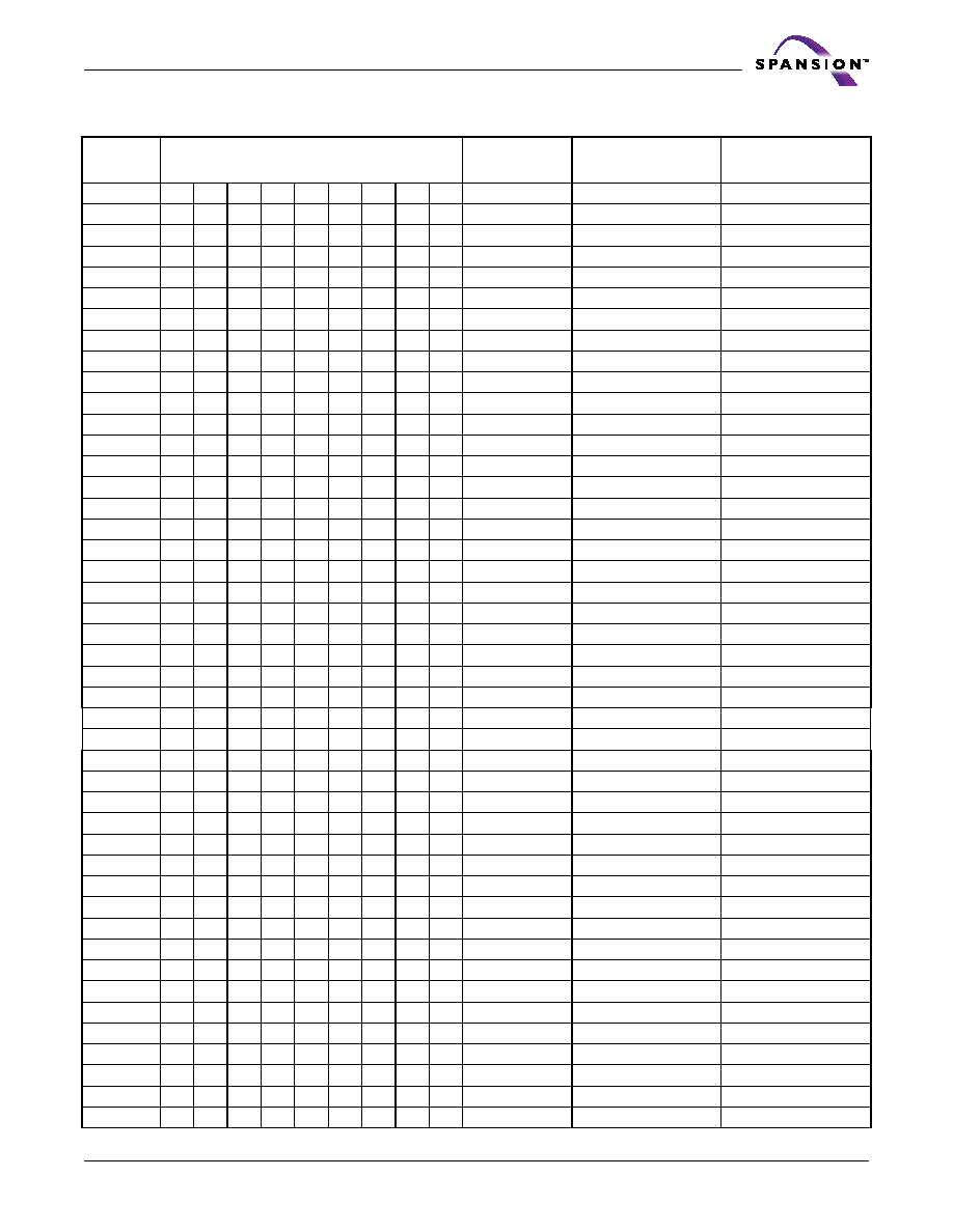
August 4, 2004 S29GLxxxM_00_B1_E
S29GLxxxM MirrorBit
TM
Flash Family
77
D a t a s h e e t
SA405
1
1
0
0
1
0
1
0
1
64/32
1950000≠195FFFF
CA8000≠CAFFFF
SA406
1
1
0
0
1
0
1
1
0
64/32
1960000≠196FFFF
CB0000≠CB7FFF
SA407
1
1
0
0
1
0
1
1
1
64/32
1970000≠197FFFF
CB8000≠CBFFFF
SA408
1
1
0
0
1
1
0
0
0
64/32
1980000≠198FFFF
CC0000≠CC7FFF
SA409
1
1
0
0
1
1
0
0
1
64/32
1990000≠199FFFF
CC8000≠CCFFFF
SA410
1
1
0
0
1
1
0
1
0
64/32
19A0000≠19AFFFF
CD0000≠CD7FFF
SA411
1
1
0
0
1
1
0
1
1
64/32
19B0000≠19BFFFF
CD8000≠CDFFFF
SA412
1
1
0
0
1
1
1
0
0
64/32
19C0000≠19CFFFF
CE0000≠CE7FFF
SA413
1
1
0
0
1
1
1
0
1
64/32
19D0000≠19DFFFF
CE8000≠CEFFFF
SA414
1
1
0
0
1
1
1
1
0
64/32
19E0000≠19EFFFF
CF0000≠CF7FFF
SA415
1
1
0
0
1
1
1
1
1
64/32
19F0000≠19FFFFF
CF8000≠CFFFFF
SA416
1
1
0
1
0
0
0
0
0
64/32
1A00000≠1A0FFFF
D00000≠D07FFF
SA417
1
1
0
1
0
0
0
0
1
64/32
1A10000≠1A1FFFF
D08000≠D0FFFF
SA418
1
1
0
1
0
0
0
1
0
64/32
1A20000≠1A2FFFF
D10000≠D17FFF
SA419
1
1
0
1
0
0
0
1
1
64/32
1A30000≠1A3FFFF
D18000≠D1FFFF
SA420
1
1
0
1
0
0
1
0
0
64/32
1A40000≠1A4FFFF
D20000≠D27FFF
SA421
1
1
0
1
0
0
1
0
1
64/32
1A50000≠1A5FFFF
D28000≠D2FFFF
SA422
1
1
0
1
0
0
1
1
0
64/32
1A60000≠1A6FFFF
D30000≠D37FFF
SA423
1
1
0
1
0
0
1
1
1
64/32
1A70000≠1A7FFFF
D38000≠D3FFFF
SA424
1
1
0
1
0
1
0
0
0
64/32
1A80000≠1A8FFFF
D40000≠D47FFF
SA425
1
1
0
1
0
1
0
0
1
64/32
1A90000≠1A9FFFF
D48000≠D4FFFF
SA426
1
1
0
1
0
1
0
1
0
64/32
1AA0000≠1AAFFFF
D50000≠D57FFF
SA427
1
1
0
1
0
1
0
1
1
64/32
1AB0000≠1ABFFFF
D58000≠D5FFFF
SA428
1
1
0
1
0
1
1
0
0
64/32
1AC0000≠1ACFFFF
D60000≠D67FFF
SA429
1
1
0
1
0
1
1
0
1
64/32
1AD0000≠1ADFFFF
D68000≠D6FFFF
SA430
1
1
0
1
0
1
1
1
0
64/32
1AE0000≠1AEFFFF
D70000≠D77FFF
SA431
1
1
0
1
0
1
1
1
1
64/32
1AF0000≠1AFFFFF
D78000≠D7FFFF
SA432
1
1
0
1
1
0
0
0
0
64/32
1B00000≠1B0FFFF
D80000≠D87FFF
SA433
1
1
0
1
1
0
0
0
1
64/32
1B10000≠1B1FFFF
D88000≠D8FFFF
SA434
1
1
0
1
1
0
0
1
0
64/32
1B20000≠1B2FFFF
D90000≠D97FFF
SA435
1
1
0
1
1
0
0
1
1
64/32
1B30000≠1B3FFFF
D98000≠D9FFFF
SA436
1
1
0
1
1
0
1
0
0
64/32
1B40000≠1B4FFFF
DA0000≠DA7FFF
SA437
1
1
0
1
1
0
1
0
1
64/32
1B50000≠1B5FFFF
DA8000≠DAFFFF
SA438
1
1
0
1
1
0
1
1
0
64/32
1B60000≠1B6FFFF
DB0000≠DB7FFF
SA439
1
1
0
1
1
0
1
1
1
64/32
1B70000≠1B7FFFF
DB8000≠DBFFFF
SA440
1
1
0
1
1
1
0
0
0
64/32
1B80000≠1B8FFFF
DC0000≠DC7FFF
SA441
1
1
0
1
1
1
0
0
1
64/32
1B90000≠1B9FFFF
DC8000≠DCFFFF
SA442
1
1
0
1
1
1
0
1
0
64/32
1BA0000≠1BAFFFF
DD0000≠DD7FFF
SA443
1
1
0
1
1
1
0
1
1
64/32
1BB0000≠1BBFFFF
DD8000≠DDFFFF
SA444
1
1
0
1
1
1
1
0
0
64/32
1BC0000≠1BCFFFF
DE0000≠DE7FFF
SA445
1
1
0
1
1
1
1
0
1
64/32
1BD0000≠1BDFFFF
DE8000≠DEFFFF
SA446
1
1
0
1
1
1
1
1
0
64/32
1BE0000≠1BEFFFF
DF0000≠DF7FFF
SA447
1
1
0
1
1
1
1
1
1
64/32
1BF0000≠1BFFFFF
DF8000≠DFFFFF
SA448
1
1
1
0
0
0
0
0
0
64/32
1C00000≠1C0FFFF
E00000≠E07FFF
SA449
1
1
1
0
0
0
0
0
1
64/32
1C10000≠1C1FFFF
E08000≠E0FFFF
Table 17. S29GL256M Sector Address Table (Continued)
Sector
A23≠A15
Sector Size
(Kbytes/
Kwords)
8-bit
Address Range
(in hexadecimal)
16-bit
Address Range
(in hexadecimal)

78
S29GLxxxM MirrorBit
TM
Flash Family
S29GLxxxM_00_B1_E August 4, 2004
D a t a s h e e t
SA450
1
1
1
0
0
0
0
1
0
64/32
1C20000≠1C2FFFF
E10000≠E17FFF
SA451
1
1
1
0
0
0
0
1
1
64/32
1C30000≠1C3FFFF
E18000≠E1FFFF
SA452
1
1
1
0
0
0
1
0
0
64/32
1C40000≠1C4FFFF
E20000≠E27FFF
SA453
1
1
1
0
0
0
1
0
1
64/32
1C50000≠1C5FFFF
E28000≠E2FFFF
SA454
1
1
1
0
0
0
1
1
0
64/32
1C60000≠1C6FFFF
E30000≠E37FFF
SA455
1
1
1
0
0
0
1
1
1
64/32
1C70000≠1C7FFFF
E38000≠E3FFFF
SA456
1
1
1
0
0
1
0
0
0
64/32
1C80000≠1C8FFFF
E40000≠E47FFF
SA457
1
1
1
0
0
1
0
0
1
64/32
1C90000≠1C9FFFF
E48000≠E4FFFF
SA458
1
1
1
0
0
1
0
1
0
64/32
1CA0000≠1CAFFFF
E50000≠E57FFF
SA459
1
1
1
0
0
1
0
1
1
64/32
1CB0000≠1CBFFFF
E58000≠E5FFFF
SA460
1
1
1
0
0
1
1
0
0
64/32
1CC0000≠1CCFFFF
E60000≠E67FFF
SA461
1
1
1
0
0
1
1
0
1
64/32
1CD0000≠1CDFFFF
E68000≠E6FFFF
SA462
1
1
1
0
0
1
1
1
0
64/32
1CE0000≠1CEFFFF
E70000≠E77FFF
SA463
1
1
1
0
0
1
1
1
1
64/32
1CF0000≠1CFFFFF
E78000≠E7FFFF
SA464
1
1
1
0
1
0
0
0
0
64/32
1D00000≠1D0FFFF
E80000≠E87FFF
SA465
1
1
1
0
1
0
0
0
1
64/32
1D10000≠1D1FFFF
E88000≠E8FFFF
SA466
1
1
1
0
1
0
0
1
0
64/32
1D20000≠1D2FFFF
E90000≠E97FFF
SA467
1
1
1
0
1
0
0
1
1
64/32
1D30000≠1D3FFFF
E98000≠E9FFFF
SA468
1
1
1
0
1
0
1
0
0
64/32
1D40000≠1D4FFFF
EA0000≠EA7FFF
SA469
1
1
1
0
1
0
1
0
1
64/32
1D50000≠1D5FFFF
EA8000≠EAFFFF
SA470
1
1
1
0
1
0
1
1
0
64/32
1D60000≠1D6FFFF
EB0000≠EB7FFF
SA471
1
1
1
0
1
0
1
1
1
64/32
1D70000≠1D7FFFF
EB8000≠EBFFFF
SA472
1
1
1
0
1
1
0
0
0
64/32
1D80000≠1D8FFFF
EC0000≠EC7FFF
SA473
1
1
1
0
1
1
0
0
1
64/32
1D90000≠1D9FFFF
EC8000≠ECFFFF
SA474
1
1
1
0
1
1
0
1
0
64/32
1DA0000≠1DAFFFF
ED0000≠ED7FFF
SA475
1
1
1
0
1
1
0
1
1
64/32
1DB0000≠1DBFFFF
ED8000≠EDFFFF
SA476
1
1
1
0
1
1
1
0
0
64/32
1DC0000≠1DCFFFF
EE0000≠EE7FFF
SA477
1
1
1
0
1
1
1
0
1
64/32
1DD0000≠1DDFFFF
EE8000≠EEFFFF
SA478
1
1
1
0
1
1
1
1
0
64/32
1DE0000≠1DEFFFF
EF0000≠EF7FFF
SA479
1
1
1
0
1
1
1
1
1
64/32
1DF0000≠1DFFFFF
EF8000≠EFFFFF
SA480
1
1
1
1
0
0
0
0
0
64/32
1E00000≠1E0FFFF
F00000≠F07FFF
SA481
1
1
1
1
0
0
0
0
1
64/32
1E10000≠1E1FFFF
F08000≠F0FFFF
SA482
1
1
1
1
0
0
0
1
0
64/32
1E20000≠1E2FFFF
F10000≠F17FFF
SA483
1
1
1
1
0
0
0
1
1
64/32
1E30000≠1E3FFFF
F18000≠F1FFFF
SA484
1
1
1
1
0
0
1
0
0
64/32
1E40000≠1E4FFFF
F20000≠F27FFF
SA485
1
1
1
1
0
0
1
0
1
64/32
1E50000≠1E5FFFF
F28000≠F2FFFF
SA486
1
1
1
1
0
0
1
1
0
64/32
1E60000≠1E6FFFF
F30000≠F37FFF
SA487
1
1
1
1
0
0
1
1
1
64/32
1E70000≠1E7FFFF
F38000≠F3FFFF
SA488
1
1
1
1
0
1
0
0
0
64/32
1E80000≠1E8FFFF
F40000≠F47FFF
SA489
1
1
1
1
0
1
0
0
1
64/32
1E90000≠1E9FFFF
F48000≠F4FFFF
SA490
1
1
1
1
0
1
0
1
0
64/32
1EA0000≠1EAFFFF
F50000≠F57FFF
SA491
1
1
1
1
0
1
0
1
1
64/32
1EB0000≠1EBFFFF
F58000≠F5FFFF
SA492
1
1
1
1
0
1
1
0
0
64/32
1EC0000≠1ECFFFF
F60000≠F67FFF
SA493
1
1
1
1
0
1
1
0
1
64/32
1ED0000≠1EDFFFF
F68000≠F6FFFF
SA494
1
1
1
1
0
1
1
1
0
64/32
1EE0000≠1EEFFFF
F70000≠F77FFF
Table 17. S29GL256M Sector Address Table (Continued)
Sector
A23≠A15
Sector Size
(Kbytes/
Kwords)
8-bit
Address Range
(in hexadecimal)
16-bit
Address Range
(in hexadecimal)

August 4, 2004 S29GLxxxM_00_B1_E
S29GLxxxM MirrorBit
TM
Flash Family
79
D a t a s h e e t
Autoselect Mode
The autoselect mode provides manufacturer and device identification, and sector group protection verification,
through identifier codes output on DQ7≠DQ0. This mode is primarily intended for programming equipment to au-
tomatically match a device to be programmed with its corresponding programming algorithm. However, the
autoselect codes can also be accessed in-system through the command register.
When using programming equipment, the autoselect mode requires VID on address pin A9. Address pins A6, A3,
A2, A1, and A0 must be as shown in Table
18
. In addition, when verifying sector protection, the sector address
must appear on the appropriate highest order address bits (see Table
6
-Table
17
). Table
18
shows the remaining
address bits that are don't care. When all necessary bits have been set as required, the programming equipment
may then read the corresponding identifier code on DQ7≠DQ0.
To access the autoselect codes in-system, the host system can issue the autoselect command via the command
register, as shown in Table
35
and Table
36
. This method does not require V
ID
. Refer to the Autoselect Command
Sequence section for more information.
SA495
1
1
1
1
0
1
1
1
1
64/32
1EF0000≠1EFFFFF
F78000≠F7FFFF
SA496
1
1
1
1
1
0
0
0
0
64/32
1F00000≠1F0FFFF
F80000≠F87FFF
SA497
1
1
1
1
1
0
0
0
1
64/32
1F10000≠1F1FFFF
F88000≠F8FFFF
SA498
1
1
1
1
1
0
0
1
0
64/32
1F20000≠1F2FFFF
F90000≠F97FFF
SA499
1
1
1
1
1
0
0
1
1
64/32
1F30000≠1F3FFFF
F98000≠F9FFFF
SA500
1
1
1
1
1
0
1
0
0
64/32
1F40000≠1F4FFFF
FA0000≠FA7FFF
SA501
1
1
1
1
1
0
1
0
1
64/32
1F50000≠1F5FFFF
FA8000≠FAFFFF
SA502
1
1
1
1
1
0
1
1
0
64/32
1F60000≠1F6FFFF
FB0000≠FB7FFF
SA503
1
1
1
1
1
0
1
1
1
64/32
1F70000≠1F7FFFF
FB8000≠FBFFFF
SA504
1
1
1
1
1
1
0
0
0
64/32
1F80000≠1F8FFFF
FC0000≠FC7FFF
SA505
1
1
1
1
1
1
0
0
1
64/32
1F90000≠1F9FFFF
FC8000≠FCFFFF
SA506
1
1
1
1
1
1
0
1
0
64/32
1FA0000≠1FAFFFF
FD0000≠FD7FFF
SA507
1
1
1
1
1
1
0
1
1
64/32
1FB0000≠1FBFFFF
FD8000≠FDFFFF
SA508
1
1
1
1
1
1
1
0
0
64/32
1FC0000≠1FCFFFF
FE0000≠FE7FFF
SA509
1
1
1
1
1
1
1
0
1
64/32
1FD0000≠1FDFFFF
FE8000≠FEFFFF
SA510
1
1
1
1
1
1
1
1
0
64/32
1FE0000≠1FEFFFF
FF0000≠FF7FFF
SA511
1
1
1
1
1
1
1
1
1
64/32
1FF0000≠1FFFFFF
FF8000≠FFFFFF
Table 17. S29GL256M Sector Address Table (Continued)
Sector
A23≠A15
Sector Size
(Kbytes/
Kwords)
8-bit
Address Range
(in hexadecimal)
16-bit
Address Range
(in hexadecimal)

80
S29GLxxxM MirrorBit
TM
Flash Family
S29GLxxxM_00_B1_E August 4, 2004
D a t a s h e e t
Table 18. Autoselect Codes, (High Voltage Method)
Legend: L = Logic Low = V
IL
, H = Logic High = V
IH
, SA = Sector Address, X = Don't care.
Description CE# OE# WE# A22 to
A15
A14
to
A10
A9
A8
to
A7
A6
A5
to
A4
A3
to
A2
A1 A0
DQ8 to DQ15
DQ7 to DQ0
Model Number
BYTE#
= V
IH
BYTE# =
V
IL
R0
R1,R2,
R8, R9
R3,R4
R5,R6,R
7
Manufacture
r ID:
Spansion
Products
L
L
H
X
X
V
ID
X
L
X
L
L
L
00
X
01h
01h
01h
01h
S29GL
256M
Cycle 1
L
L
H
X
X
V
ID
X
L
X
L
L
H
22
X
7Eh
Cycle 2
H
H
L
22
X
12h
Cycle 3
H
H
H
22
X
01h
S29GL
128M
Cycle 1
L
L
H
X
X
V
ID
X
L
X
L
L
H
22
X
7Eh
Cycle 2
H
H
L
22
X
12h
Cycle 3
H
H
H
22
X
00h
S29GL
064M
Cycle 1
L
L
H
X
X
V
ID
X
L
X
L
L
H
22
X
7Eh
7Eh
7Eh
7Eh
Cycle 2
H
H
L
22
X
13h
0Ch
10h
13h
Cycle 3
H
H
H
22
X
00h
01h
00h (-R4,
bottom boot)
01h (-R3, top
boot)
01h
S29GL
032M
Cycle 1
L
L
H
X
X
V
ID
X
L
X
L
L
H
22
X
7Eh
7Eh
7Eh
7Eh
Cycle 2
H
H
L
22
X
1Ch
1Dh
1Ah
1Ah
Cycle 3
H
H
H
22
X
00h
00h
00h (-R4,
bottom boot)
01h (-R3, top
boot)
00h (-R6
bottom
boot)
01h (-
R5, top
boot)
Sector Group
Protection
Verification
L
L
H
SA
X
V
ID
X
L
X
L
H
L
X
X
01h (protected),
00h (unprotected)
SecSi Sector
Indicator Bit
(DQ7), WP#
protects
highest
address
sector
L
L
H
X
X
V
ID
X
L
X
L
H
H
X
X
98h (factory locked),
18h (not factory locked)
SecSi Sector
Indicator Bit
(DQ7), WP#
protects
lowest
address
sector
L
L
H
X
X
V
ID
X
L
X
L
H
H
X
X
88h (factory locked),
08h (not factory locked)
August 4, 2004 S29GLxxxM_00_B1_E
S29GLxxxM MirrorBit
TM
Flash Family
81
D a t a s h e e t
Sector Group Protection and Unprotection
The hardware sector group protection feature disables both program and erase operations in any sector group.
In this device, a sector group consists of four adjacent sectors that are protected or unprotected at the same time
(see
Table 4
). The hardware sector group unprotection feature re-enables both program and erase operations in
previously protected sector groups. Sector group protection/unprotection can be implemented via two methods.
Sector protection/unprotection requires V
ID
on the RESET# pin only, and can be implemented either in-system or
via programming equipment. Figure 2 shows the algorithms and Figure 24 shows the timing diagram. This method
uses standard microprocessor bus cycle timing. For sector group unprotect, all unprotected sector groups must
first be protected prior to the first sector group unprotect write cycle.
The device is shipped with all sector groups unprotected. Spansion offers the option of programming and protect-
ing sector groups at its factory prior to shipping the device through Spansion Programming Service. Contact a
Spansion representative for details.
It is possible to determine whether a sector group is protected or unprotected. See the
Autoselect Mode
section
for details.
Table 19. S29GL032M (Model R0) Sector Group Protection/Unprotection Address Table
Note: All sector groups are 256 Kbytes in size.
Sector Group
A22≠A18
SA0≠SA3
00000
SA4≠SA7
00001
SA8≠SA11
00010
SA12≠SA15
00011
SA16≠SA19
00100
SA20≠SA23
00101
SA24≠SA27
00110
SA28≠SA31
00111
SA32≠SA35
01000
SA36≠SA39
01001
SA40≠SA43
01010
SA44≠SA47
01011
SA48≠SA51
01100
SA52≠SA55
01101
SA56≠SA59
01110
SA60≠SA63
01111
82
S29GLxxxM MirrorBit
TM
Flash Family
S29GLxxxM_00_B1_E August 4, 2004
D a t a s h e e t
Table 20. S29GL032M (Model R1) Top Boot Sector Protection
Sector
A20≠A12
Sector/
Sector Block Size
SA0-SA3
0000XXXXXh
256 (4x64) Kbytes
SA4-SA7
0001XXXXXh
256 (4x64) Kbytes
SA8-SA11
0010XXXXXh
256 (4x64) Kbytes
SA12-SA15
0011XXXXXh
256 (4x64) Kbytes
SA16-SA19
0100XXXXXh
256 (4x64) Kbytes
SA20-SA23
0101XXXXXh
256 (4x64) Kbytes
SA24-SA27
0110XXXXXh
256 (4x64) Kbytes
SA28-SA31
0111XXXXXh
256 (4x64) Kbytes
SA32≠SA35
1000XXXXXh,
256 (4x64) Kbytes
SA36≠SA39
1001XXXXXh
256 (4x64) Kbytes
SA40≠SA43
1010XXXXXh
256 (4x64) Kbytes
SA44≠SA47
1011XXXXXh
256 (4x64) Kbytes
SA48≠SA51
1100XXXXXh
256 (4x64) Kbytes
SA52-SA55
1101XXXXXh
256 (4x64) Kbytes
SA56-SA59
1110XXXXXh
256 (4x64) Kbytes
SA60-SA62
111100XXXh
111101XXXh
111110XXXh
192 (3x64) Kbytes
SA63
111111000h
8 Kbytes
SA64
111111001h
8 Kbytes
SA65
111111010h
8 Kbytes
SA66
111111011h
8 Kbytes
SA67
111111100h
8 Kbytes
SA68
111111101h
8 Kbytes
SA69
111111110h
8 Kbytes
SA70
111111111h
8 Kbytes

August 4, 2004 S29GLxxxM_00_B1_E
S29GLxxxM MirrorBit
TM
Flash Family
83
D a t a s h e e t
Table 22. S29GL032M (Models R3, R4) Sector Group Protection/Unprotection Address Table
Table 21. S29GL032M (Model R2) Bottom Boot Sector Protection
Sector
A20≠A12
Sector/
Sector Block Size
SA0
000000000h
8 Kbytes
SA1
000000001h
8 Kbytes
SA2
000000010h
8 Kbytes
SA3
000000011h
8 Kbytes
SA4
000000100h
8 Kbytes
SA5
000000101h
8 Kbytes
SA6
000000110h
8 Kbytes
SA7
000000111h
8 Kbytes
SA8≠SA10
000001XXXh,
000010XXXh,
000011XXXh,
192 (3x64) Kbytes
SA11≠SA14
0001XXXXXh
256 (4x64) Kbytes
SA15≠SA18
0010XXXXXh
256 (4x64) Kbytes
SA19≠SA22
0011XXXXXh
256 (4x64) Kbytes
SA23≠SA26
0100XXXXXh
256 (4x64) Kbytes
SA27-SA30
0101XXXXXh
256 (4x64) Kbytes
SA31-SA34
0110XXXXXh
256 (4x64) Kbytes
SA35-SA38
0111XXXXXh
256 (4x64) Kbytes
SA39-SA42
1000XXXXXh
256 (4x64) Kbytes
SA43-SA46
1001XXXXXh
256 (4x64) Kbytes
SA47-SA50
1010XXXXXh
256 (4x64) Kbytes
SA51-SA54
1011XXXXXh
256 (4x64) Kbytes
SA55≠SA58
1100XXXXXh
256 (4x64) Kbytes
SA59≠SA62
1101XXXXXh
256 (4x64) Kbytes
SA63≠SA66
1110XXXXXh
256 (4x64) Kbytes
SA67≠SA70
1111XXXXXh
256 (4x64) Kbytes
Sector Group
A20≠A15
SA0
000000
SA1
000001
SA2
000010
SA3
000011
SA4≠SA7
0001xx
SA8≠SA11
0010xx
SA12≠SA15
0011xx
SA16≠SA19
0100xx
SA20≠SA23
0101xx
SA24≠SA27
0110xx
SA28≠SA31
0111xx
SA32≠SA35
1000xx
SA36≠SA39
1001xx
SA40≠SA43
1010xx
SA44≠SA47
1011xx
84
S29GLxxxM MirrorBit
TM
Flash Family
S29GLxxxM_00_B1_E August 4, 2004
D a t a s h e e t
Table 23. S29GL065M (Model 00) Sector Group Protection/Unprotection Address Table
Note: All sector groups are 256 Kbytes in size.
SA48≠SA51
1100xx
SA52≠SA55
1101xx
SA56≠SA59
1110xx
SA60
111100
SA61
111101
SA62
111110
SA63
111111
Sector Group
A22≠A18
SA0≠SA3
00000
SA4≠SA7
00001
SA8≠SA11
00010
SA12≠SA15
00011
SA16≠SA19
00100
SA20≠SA23
00101
SA24≠SA27
00110
SA28≠SA31
00111
SA32≠SA35
01000
SA36≠SA39
01001
SA40≠SA43
01010
SA44≠SA47
01011
SA48≠SA51
01100
SA52≠SA55
01101
SA56≠SA59
01110
SA60≠SA63
01111
SA64≠SA67
10000
SA68≠SA71
10001
SA72≠SA75
10010
SA76≠SA79
10011
SA80≠SA83
10100
SA84≠SA87
10101
SA88≠SA91
10110
SA92≠SA95
10111
SA96≠SA99
11000
SA100≠SA103
11001
SA104≠SA107
11010
SA108≠SA111
11011
SA112≠SA115
11100
SA116≠SA119
11101
SA120≠SA123
11110
SA124≠SA127
11111
Sector Group
A20≠A15
August 4, 2004 S29GLxxxM_00_B1_E
S29GLxxxM MirrorBit
TM
Flash Family
85
D a t a s h e e t
Table 24.
S29GL064M (Model R1) Top Boot Sector Protection
Sector
A21≠A12
Sector/
Sector Block Size
SA0-SA3
00000XXXXX
256 (4x64) Kbytes
SA4-SA7
00001XXXXX
256 (4x64) Kbytes
SA8-SA11
00010XXXXX
256 (4x64) Kbytes
SA12-SA15
00011XXXXX
256 (4x64) Kbytes
SA16-SA19
00100XXXXX
256 (4x64) Kbytes
SA20-SA23
00101XXXXX
256 (4x64) Kbytes
SA24-SA27
00110XXXXX
256 (4x64) Kbytes
SA28-SA31
00111XXXXX
256 (4x64) Kbytes
SA32-SA35
01000XXXXX
256 (4x64) Kbytes
SA36-SA39
01001XXXXX
256 (4x64) Kbytes
SA40-SA43
01010XXXXX
256 (4x64) Kbytes
SA44-SA47
01011XXXXX
256 (4x64) Kbytes
SA48-SA51
01100XXXXX
256 (4x64) Kbytes
SA52-SA55
01101XXXXX
256 (4x64) Kbytes
SA56-SA59
01110XXXXX
256 (4x64) Kbytes
SA60-SA63
01111XXXXX
256 (4x64) Kbytes
SA64-SA67
10000XXXXX
256 (4x64) Kbytes
SA68-SA71
10001XXXXX
256 (4x64) Kbytes
SA72-SA75
10010XXXXX
256 (4x64) Kbytes
SA76-SA79
10011XXXXX
256 (4x64) Kbytes
SA80-SA83
10100XXXXX
256 (4x64) Kbytes
SA84-SA87
10101XXXXX
256 (4x64) Kbytes
SA88-SA91
10110XXXXX
256 (4x64) Kbytes
SA92-SA95
10111XXXXX
256 (4x64) Kbytes
SA96-SA99
11000XXXXX
256 (4x64) Kbytes
SA100-SA103
11001XXXXX
256 (4x64) Kbytes
SA104-SA107
11010XXXXX
256 (4x64) Kbytes
SA108-SA111
11011XXXXX
256 (4x64) Kbytes
SA112-SA115
11100XXXXX
256 (4x64) Kbytes
SA116-SA119
11101XXXXX
256 (4x64) Kbytes
SA120-SA123
11110XXXXX
256 (4x64) Kbytes
SA124-SA126
1111100XXX
1111101XXX
1111110XXX
192 (3x64) Kbytes
SA127
1111111000
8 Kbytes
SA128
1111111001
8 Kbytes
SA129
1111111010
8 Kbytes
SA130
1111111011
8 Kbytes
SA131
1111111100
8 Kbytes
SA132
1111111101
8 Kbytes
SA133
1111111110
8 Kbytes
SA134
1111111111
8 Kbytes
86
S29GLxxxM MirrorBit
TM
Flash Family
S29GLxxxM_00_B1_E August 4, 2004
D a t a s h e e t
Table 25. S29GL064M (Model R2) Bottom Boot Sector Protection
Sector
A21≠A12
Sector/
Sector Block Size
SA0
0000000000
8 Kbytes
SA1
0000000001
8 Kbytes
SA2
0000000010
8 Kbytes
SA3
0000000011
8 Kbytes
SA4
0000000100
8 Kbytes
SA5
0000000101
8 Kbytes
SA6
0000000110
8 Kbytes
SA7
0000000111
8 Kbytes
SA8≠SA10
0000001XXX,
0000010XXX,
0000011XXX,
192 (3x64) Kbytes
SA11≠SA14
00001XXXXX
256 (4x64) Kbytes
SA15≠SA18
00010XXXXX
256 (4x64) Kbytes
SA19≠SA22
00011XXXXX
256 (4x64) Kbytes
SA23≠SA26
00100XXXXX
256 (4x64) Kbytes
SA27-SA30
00101XXXXX
256 (4x64) Kbytes
SA31-SA34
00110XXXXX
256 (4x64) Kbytes
SA35-SA38
00111XXXXX
256 (4x64) Kbytes
SA39-SA42
01000XXXXX
256 (4x64) Kbytes
SA43-SA46
01001XXXXX
256 (4x64) Kbytes
SA47-SA50
01010XXXXX
256 (4x64) Kbytes
SA51-SA54
01011XXXXX
256 (4x64) Kbytes
SA55≠SA58
01100XXXXX
256 (4x64) Kbytes
SA59≠SA62
01101XXXXX
256 (4x64) Kbytes
SA63≠SA66
01110XXXXX
256 (4x64) Kbytes
SA67≠SA70
01111XXXXX
256 (4x64) Kbytes
SA71≠SA74
10000XXXXX
256 (4x64) Kbytes
SA75≠SA78
10001XXXXX
256 (4x64) Kbytes
SA79≠SA82
10010XXXXX
256 (4x64) Kbytes
SA83≠SA86
10011XXXXX
256 (4x64) Kbytes
SA87≠SA90
10100XXXXX
256 (4x64) Kbytes
SA91≠SA94
10101XXXXX
256 (4x64) Kbytes
SA95≠SA98
10110XXXXX
256 (4x64) Kbytes
SA99≠SA102
10111XXXXX
256 (4x64) Kbytes
SA103≠SA106
11000XXXXX
256 (4x64) Kbytes
SA107≠SA110
11001XXXXX
256 (4x64) Kbytes
SA111≠SA114
11010XXXXX
256 (4x64) Kbytes
SA115≠SA118
11011XXXXX
256 (4x64) Kbytes
SA119≠SA122
11100XXXXX
256 (4x64) Kbytes
SA123≠SA126
11101XXXXX
256 (4x64) Kbytes
SA127≠SA130
11110XXXXX
256 (4x64) Kbytes
SA131≠SA134
11111XXXXX
256 (4x64) Kbytes

August 4, 2004 S29GLxxxM_00_B1_E
S29GLxxxM MirrorBit
TM
Flash Family
87
D a t a s h e e t
Table 26. S29GL064M (Models R3, R4) Sector Group Protection/Unprotection Address Table
Sector Group
A21≠A15
SA0
0000000
SA1
0000001
SA2
0000010
SA3
0000011
SA4≠SA7
00001xx
SA8≠SA11
00010xx
SA12≠SA15
00011xx
SA16≠SA19
00100xx
SA20≠SA23
00101xx
SA24≠SA27
00110xx
SA28≠SA31
00111xx
SA32≠SA35
01000xx
SA36≠SA39
01001xx
SA40≠SA43
01010xx
SA44≠SA47
01011xx
SA48≠SA51
01100xx
SA52≠SA55
01101xx
SA56≠SA59
01110xx
SA60≠SA63
01111xx
SA64≠SA67
10000xx
SA68≠SA71
10001xx
SA72≠SA75
10010xx
SA76≠SA79
10011xx
SA80≠SA83
10100xx
SA84≠SA87
10101xx
SA88≠SA91
10110xx
SA92≠SA95
10111xx
SA96≠SA99
11000xx
SA100≠SA103
11001xx
SA104≠SA107
11010xx
SA108≠SA111
11011xx
SA112≠SA115
11100xx
SA116≠SA119
11101xx
SA120≠SA123
11110xx
SA124
1111100
SA125
1111101
SA126
1111110
SA127
1111111

88
S29GLxxxM MirrorBit
TM
Flash Family
S29GLxxxM_00_B1_E August 4, 2004
D a t a s h e e t
Table 27. S29GL064M (Model R5) Sector Group Protection/Unprotection Address Table
Note: All sector groups are 128 Kwords in size.
Sector Group
A21≠A17
SA0≠SA3
00000
SA4≠SA7
00001
SA8≠SA11
00010
SA12≠SA15
00011
SA16≠SA19
00100
SA20≠SA23
00101
SA24≠SA27
00110
SA28≠SA31
00111
SA32≠SA35
01000
SA36≠SA39
01001
SA40≠SA43
01010
SA44≠SA47
01011
SA48≠SA51
01100
SA52≠SA55
01101
SA56≠SA59
01110
SA60≠SA63
01111
SA64≠SA67
10000
SA68≠SA71
10001
SA72≠SA75
10010
SA76≠SA79
10011
SA80≠SA83
10100
SA84≠SA87
10101
SA88≠SA91
10110
SA92≠SA95
10111
SA96≠SA99
11000
SA100≠SA103
11001
SA104≠SA107
11010
SA108≠SA111
11011
SA112≠SA115
11100
SA116≠SA119
11101
SA120≠SA123
11110
SA124≠SA127
11111

August 4, 2004 S29GLxxxM_00_B1_E
S29GLxxxM MirrorBit
TM
Flash Family
89
D a t a s h e e t
Table 28. S29GL064M (Models R6, R7) Sector Group Protection/Unprotection Address Table
Note: All sector groups are 128 Kwords in size.
Sector Group
A21≠A17
SA0≠SA3
00000
SA4≠SA7
00001
SA8≠SA11
00010
SA12≠SA15
00011
SA16≠SA19
00100
SA20≠SA23
00101
SA24≠SA27
00110
SA28≠SA31
00111
SA32≠SA35
01000
SA36≠SA39
01001
SA40≠SA43
01010
SA44≠SA47
01011
SA48≠SA51
01100
SA52≠SA55
01101
SA56≠SA59
01110
SA60≠SA63
01111
SA64≠SA67
10000
SA68≠SA71
10001
SA72≠SA75
10010
SA76≠SA79
10011
SA80≠SA83
10100
SA84≠SA87
10101
SA88≠SA91
10110
SA92≠SA95
10111
SA96≠SA99
11000
SA100≠SA103
11001
SA104≠SA107
11010
SA108≠SA111
11011
SA112≠SA115
11100
SA116≠SA119
11101
SA120≠SA123
11110
SA124≠SA127
11111
90
S29GLxxxM MirrorBit
TM
Flash Family
S29GLxxxM_00_B1_E August 4, 2004
D a t a s h e e t
Table 29. S29GL128M Sector Group Protection/Unprotection Address Table
Sector Group
A22≠A15
SA0
00000000
SA1
00000001
SA2
00000010
SA3
00000011
SA4≠SA7
000001xx
SA8≠SA11
000010xx
SA12≠SA15
000011xx
SA16≠SA19
000100xx
SA20≠SA23
000101xx
SA24≠SA27
000110xx
SA28≠SA31
000111xx
SA32≠SA35
001000xx
SA36≠SA39
001001xx
SA40≠SA43
001010xx
SA44≠SA47
001011xx
SA48≠SA51
001100xx
SA52≠SA55
001101xx
SA56≠SA59
001110xx
SA60≠SA63
001111xx
SA64≠SA67
010000xx
SA68≠SA71
010001xx
SA72≠SA75
010010xx
SA76≠SA79
010011xx
SA80≠SA83
010100xx
SA84≠SA87
010101xx
SA88≠SA91
010110xx
SA92≠SA95
010111xx
SA96≠SA99
011000xx
SA100≠SA103
011001xx
SA104≠SA107
011010xx
SA108≠SA111
011011xx
SA112≠SA115
011100xx
SA116≠SA119
011101xx
SA120≠SA123
011110xx
SA124≠SA127
011111xx
SA128≠SA131
100000xx
SA132≠SA135
100001xx
SA136≠SA139
100010xx
SA140≠SA143
100011xx
SA144≠SA147
100100xx
SA148≠SA151
100101xx
August 4, 2004 S29GLxxxM_00_B1_E
S29GLxxxM MirrorBit
TM
Flash Family
91
D a t a s h e e t
SA152≠SA155
100110xx
SA156≠SA159
100111xx
SA160≠SA163
101000xx
SA164≠SA167
101001xx
SA168≠SA171
101010xx
SA172≠SA175
101011xx
SA176≠SA179
101100xx
SA180≠SA183
101101xx
SA184≠SA187
101110xx
SA188≠SA191
101111xx
SA192≠SA195
110000xx
SA196≠SA199
110001xx
SA200≠SA203
110010xx
SA204≠SA207
110011xx
SA208≠SA211
110100xx
SA212≠SA215
110101xx
SA216≠SA219
110110xx
SA220≠SA223
110111xx
SA224≠SA227
111000xx
SA228≠SA231
111001xx
SA232≠SA235
111010xx
SA236≠SA239
111011xx
SA240≠SA243
111100xx
SA244≠SA247
111101xx
SA248≠SA251
111110xx
SA252
11111100
SA253
11111101
SA254
11111110
SA255
11111111
Table 29. S29GL128M Sector Group Protection/Unprotection Address Table (Continued)
Sector Group
A22≠A15

92
S29GLxxxM MirrorBit
TM
Flash Family
S29GLxxxM_00_B1_E August 4, 2004
D a t a s h e e t
Table 30. S29GL256M Sector Group Protection/Unprotection Address Table
Sector Group
A23≠A15
SA0
000000000
SA1
000000001
SA2
000000010
SA3
000000011
SA4≠SA7
0000001xx
SA8≠SA11
0000010xx
SA12≠SA15
0000011xx
SA16≠SA19
0000100xx
SA20≠SA23
0000101xx
SA24≠SA27
0000110xx
SA28≠SA31
0000111xx
SA32≠SA35
0001000xx
SA36≠SA39
0001001xx
SA40≠SA43
0001010xx
SA44≠SA47
0001011xx
SA48≠SA51
0001100xx
SA52≠SA55
0001101xx
SA56≠SA59
0001110xx
SA60≠SA63
0001111xx
SA64≠SA67
0010000xx
SA68≠SA71
0010001xx
SA72≠SA75
0010010xx
SA76≠SA79
0010011xx
SA80≠SA83
0010100xx
SA84≠SA87
0010101xx
SA88≠SA91
0010110xx
SA92≠SA95
0010111xx
SA96≠SA99
0011000xx
SA100≠SA103
0011001xx
SA104≠SA107
0011010xx
SA108≠SA111
0011011xx
SA112≠SA115
0011100xx
SA116≠SA119
0011101xx
SA120≠SA123
0011110xx
SA124≠SA127
0011111xx
SA128≠SA131
0100000xx
SA132≠SA135
0100001xx
SA136≠SA139
0100010xx
SA140≠SA143
0100011xx
SA144≠SA147
0100100xx
SA148≠SA151
0100101xx

August 4, 2004 S29GLxxxM_00_B1_E
S29GLxxxM MirrorBit
TM
Flash Family
93
D a t a s h e e t
SA152≠SA155
0100110xx
SA156≠SA159
0100111xx
SA160≠SA163
0101000xx
SA164≠SA167
0101001xx
SA168≠SA171
0101010xx
SA172≠SA175
0101011xx
SA176≠SA179
0101100xx
SA180≠SA183
0101101xx
SA184≠SA187
0101110xx
SA188≠SA191
0101111xx
SA192≠SA195
0110000xx
SA196≠SA199
0110001xx
SA200≠SA203
0110010xx
SA204≠SA207
0110011xx
SA208≠SA211
0110100xx
SA212≠SA215
0110101xx
SA216≠SA219
0110110xx
SA220≠SA223
0110111xx
SA224≠SA227
0111000xx
SA228≠SA231
0111001xx
SA232≠SA235
0111010xx
SA236≠SA239
0111011xx
SA240≠SA243
0111100xx
SA244≠SA247
0111101xx
SA248≠SA251
0111110xx
SA252≠SA255
0111111xx
SA256≠SA259
1000000xx
SA260≠SA263
1000001xx
SA264≠SA267
1000010xx
SA268≠SA271
1000011xx
SA272≠SA275
1000100xx
SA276≠SA279
1000101xx
SA280≠SA283
1000110xx
SA284≠SA287
1000111xx
SA288≠SA291
1001000xx
SA292≠SA295
1001001xx
SA296≠SA299
1001010xx
SA300≠SA303
1001011xx
SA304≠SA307
1001100xx
SA308≠SA311
1001101xx
SA312≠SA315
1001110xx
Table 30. S29GL256M Sector Group Protection/Unprotection Address Table (Continued)
Sector Group
A23≠A15

94
S29GLxxxM MirrorBit
TM
Flash Family
S29GLxxxM_00_B1_E August 4, 2004
D a t a s h e e t
SA316≠SA319
1001111xx
SA320≠SA323
1010000xx
SA324≠SA327
1010001xx
SA328≠SA331
1010010xx
SA332≠SA335
1010011xx
SA336≠SA339
1010100xx
SA340≠SA343
1010101xx
SA344≠SA347
1010110xx
SA348≠SA351
1010111xx
SA352≠SA355
1011000xx
SA356≠SA359
1011001xx
SA360≠SA363
1011010xx
SA364≠SA367
1011011xx
SA368≠SA371
1011100xx
SA372≠SA375
1011101xx
SA376≠SA379
1011110xx
SA380≠SA383
1011111xx
SA384≠SA387
1100000xx
SA388≠SA391
1100001xx
SA392≠SA395
1100010xx
SA396≠SA399
1100011xx
SA400≠SA403
1100100xx
SA404≠SA407
1100101xx
SA408≠SA411
1100110xx
SA412≠SA415
1100111xx
SA416≠SA419
1101000xx
SA420≠SA423
1101001xx
SA424≠SA427
1101010xx
SA428≠SA431
1101011xx
SA432≠SA435
1101100xx
SA436≠SA439
1101101xx
SA440≠SA443
1101110xx
SA444≠SA447
1101111xx
SA448≠SA451
1110000xx
SA452≠SA455
1110001xx
SA456≠SA459
1110010xx
SA460≠SA463
1110011xx
SA464≠SA467
1110100xx
SA468≠SA471
1110101xx
SA472≠SA475
1110110xx
SA476≠SA479
1110111xx
Table 30. S29GL256M Sector Group Protection/Unprotection Address Table (Continued)
Sector Group
A23≠A15

August 4, 2004 S29GLxxxM_00_B1_E
S29GLxxxM MirrorBit
TM
Flash Family
95
D a t a s h e e t
Temporary Sector Group Unprotect
This feature allows temporary unprotection of previously protected sector groups to change data in-system. The
Sector Group Unprotect mode is activated by setting the RESET# pin to
V
ID
. During this mode, formerly protected
sector groups can be programmed or erased by selecting the sector group addresses. Once V
ID
is removed from
the RESET# pin, all the previously protected sector groups are protected again. Figure 1 shows the algorithm,
and Figure 23 shows the timing diagrams, for this feature.
Notes:
1. All protected sector groups unprotected (If WP# = V
IL
, the first or last sector will remain protected).
2. All previously protected sector groups are protected once again.
Figure 1. Temporary Sector Group Unprotect Operation
SA480≠SA483
1111000xx
SA484≠SA487
1111001xx
SA488≠SA491
1111010xx
SA492≠SA495
1111011xx
SA496≠SA499
1111100xx
SA500≠SA503
1111101xx
SA504≠SA507
1111110xx
SA508
111111100
SA509
111111101
SA510
111111110
SA511
111111111
Table 30. S29GL256M Sector Group Protection/Unprotection Address Table (Continued)
Sector Group
A23≠A15
START
Perform Erase or
Program Operations
RESET# = V
IH
Temporary Sector
Group Unprotect Completed
(Note 2)
RESET# = V
ID
(Note 1)
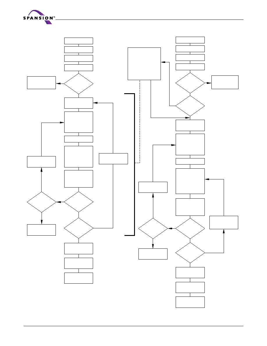
96
S29GLxxxM MirrorBit
TM
Flash Family
S29GLxxxM_00_B1_E August 4, 2004
D a t a s h e e t
Figure 2. In-System Sector Group Protect/Unprotect Algorithms
Sector Group Protect:
Write 60h to sector
group address with
A6≠A0 = 0xx0010
Set up sector
group address
Wait 150 µs
Verify Sector Group
Protect: Write 40h
to sector group
address with
A6≠A0 = 0xx0010
Read from
sector group address
with A6≠A0
= 0xx0010
START
PLSCNT = 1
RESET# = V
ID
Wait 1
µs
First Write
Cycle = 60h?
Data = 01h?
Remove V
ID
from RESET#
Write reset
command
Sector Group
Protect complete
Yes
Yes
No
PLSCNT
= 25?
Yes
Device failed
Increment
PLSCNT
Temporary Sector
Group Unprotect
Mode
No
Sector Group
Unprotect:
Write 60h to sector
group address with
A6≠A0 = 1xx0010
Set up first sector
group address
Wait 15 ms
Verify Sector Group
Unprotect: Write
40h to sector group
address with
A6≠A0 = 1xx0010
Read from
sector group
address with
A6≠A0 = 1xx0010
START
PLSCNT = 1
RESET# = V
ID
Wait 1
µs
Data = 00h?
Last sector
group
verified?
Remove V
ID
from RESET#
Write reset
command
Sector Group
Unprotect complete
Yes
No
PLSCNT
= 1000?
Yes
Device failed
Increment
PLSCNT
Temporary Sector
Group Unprotect
Mode
No
All sector
groups
protected?
Yes
Protect all sector
groups: The indicated
portion of the sector
group protect algorithm
must be performed for all
unprotected sector
groups prior to issuing
the first sector group
unprotect address
Set up
next sector group
address
No
Yes
No
Yes
No
No
Yes
No
Sector Group
Protect
Algorithm
Sector Group
Unprotect
Algorithm
First Write
Cycle = 60h?
Protect
another
sector group?
Reset
PLSCNT = 1

August 4, 2004 S29GLxxxM_00_B1_E
S29GLxxxM MirrorBit
TM
Flash Family
97
D a t a s h e e t
SecSi (Secured Silicon) Sector Flash Memory Region
The SecSi (Secured Silicon) Sector feature provides a Flash memory region that enables permanent part identi-
fication through an Electronic Serial Number (ESN). The SecSi Sector is 256 bytes in length, and uses a SecSi
Sector Indicator Bit (DQ7) to indicate whether or not the SecSi Sector is locked when shipped from the factory.
This bit is permanently set at the factory and cannot be changed, which prevents cloning of a factory locked part.
This ensures the security of the ESN once the product is shipped to the field.
The factory offers the device with the SecSi Sector either customer lockable (standard shipping option) or factory
locked (contact a Spansion sales representative for ordering information). The customer-lockable version is
shipped with the SecSi Sector unprotected, allowing customers to program the sector after receiving the device.
The customer-lockable version also has the SecSi Sector Indicator Bit permanently set to a "0." The factory-locked
version is always protected when shipped from the factory, and has the SecSi (Secured Silicon) Sector Indicator
Bit permanently set to a "1." Thus, the SecSi Sector Indicator Bit prevents customer-lockable devices from being
used to replace devices that are factory locked. Note that the ACC function and unlock bypass modes are not
available when the SecSi Sector is enabled.
The SecSi sector address space in this device is allocated as follows:
The system accesses the SecSi Sector through a command sequence (see "Write Protect (WP#)"). After the sys-
tem has written the Enter SecSi Sector command sequence, it may read the SecSi Sector by using the addresses
normally occupied by the first sector (SA0). This mode of operation continues until the system issues the Exit
SecSi Sector command sequence, or until power is removed from the device. On power-up, or following a hard-
ware reset, the device reverts to sending commands to sector SA0.
Customer Lockable: SecSi Sector NOT Programmed or Protected At the Factory
Unless otherwise specified, the device is shipped such that the customer may program and protect the 256-byte
SecSi sector.
The system may program the SecSi Sector using the write-buffer, accelerated and/or unlock bypass methods, in
addition to the standard programming command sequence. See Command Definitions.
Programming and protecting the SecSi Sector must be used with caution since, once protected, there is no pro-
cedure available for unprotecting the SecSi Sector area and none of the bits in the SecSi Sector memory space
can be modified in any way.
The SecSi Sector area can be protected using one of the following procedures:
Write the three-cycle Enter SecSi Sector Region command sequence, and then follow the in-system
sector protect algorithm as shown in
Figure 2
, except that RESET# may be at either V
IH
or V
ID
. This
allows in-system protection of the SecSi Sector without raising any device pin to a high voltage. Note
that this method is only applicable to the SecSi Sector.
To verify the protect/unprotect status of the SecSi Sector, follow the algorithm shown in
Figure 1
.
Once the SecSi Sector is programmed, locked and verified, the system must write the Exit SecSi Sector Region
command sequence to return to reading and writing within the remainder of the array.
SecSi Sector Address
Range
Customer Lockable
ESN Factory Locked
ExpressFlash
Factory Locked
000000h≠000007h
Determined by
customer
ESN
ESN or determined by
customer
000008h≠00007Fh
Unavailable
Determined by
customer

98
S29GLxxxM MirrorBit
TM
Flash Family
S29GLxxxM_00_B1_E August 4, 2004
D a t a s h e e t
Factory Locked: SecSi Sector Programmed and Protected At the Factory
In devices with an ESN, the SecSi Sector is protected when the device is shipped from the factory. The SecSi Sec-
tor cannot be modified in any way. An ESN Factory Locked device has an 16-byte random ESN at addresses
000000h≠000007h. Please contact your sales representative for details on ordering ESN Factory Locked devices.
Customers may opt to have their code programmed by the factory through the Spansion programming service
(Customer Factory Locked). The devices are then shipped from the factory with the SecSi Sector permanently
locked. Contact your sales representative for details on using the Spansion programming service.
Write Protect (WP#)
The Write Protect function provides a hardware method of protecting the first or last sector group without using
V
ID
. Write Protect is one of two functions provided by the WP#/ACC input.
If the system asserts V
IL
on the WP#/ACC pin, the device disables program and erase functions in the first or last
sector group independently of whether those sector groups were protected or unprotected. Note that if WP#/ACC
is at V
IL
when the device is in the standby mode, the maximum input load current is increased. See the table in
"DC Characteristics" section on page 122.
Note: If the system asserts V
IH
on the WP#/ACC pin, the device reverts to whether the first or last sector was
previously set to be protected or unprotected using the method described in "Sector Group Protection and
Unprotection". Note that WP# has an internal pullup; when unconnected, WP# is at V
IH
.
Hardware Data Protection
The command sequence requirement of unlock cycles for programming or erasing provides data protection
against inadvertent writes (refer to Tables
16
and
17
for command definitions). In addition, the following hardware
data protection measures prevent accidental erasure or programming, which might otherwise be caused by spu-
rious system level signals during V
CC
power-up and power-down transitions, or from system noise.
Low V
CC
Write Inhibit
When V
CC
is less than V
LKO
, the device does not accept any write cycles. This protects data during V
CC
power-up
and power-down. The command register and all internal program/erase circuits are disabled, and the device re-
sets to the read mode. Subsequent writes are ignored until V
CC
is greater than V
LKO
. The system must provide
the proper signals to the control pins to prevent unintentional writes when V
CC
is greater than V
LKO
.
Write Pulse "Glitch" Protection
Noise pulses of less than 3 ns (typical) on OE#, CE# or WE# do not initiate a write cycle.
Logical Inhibit
Write cycles are inhibited by holding any one of OE# = V
IL
, CE# = V
IH
or WE# = V
IH
. To initiate a write cycle,
CE# and WE# must be a logical zero while OE# is a logical one.
Power-Up Write Inhibit
If WE# = CE# = V
IL
and OE# = V
IH
during power up, the device does not accept commands on the rising edge
of WE#. The internal state machine is automatically reset to the read mode on power-up.

August 4, 2004 S29GLxxxM_00_B1_E
S29GLxxxM MirrorBit
TM
Flash Family
99
D a t a s h e e t
Common Flash Memory Interface (CFI)
The Common Flash Interface (CFI) specification outlines device and host system software interrogation hand-
shake, which allows specific vendor-specified software algorithms to be used for entire families of devices.
Software support can then be device-independent, JEDEC ID-independent, and forward- and backward-compat-
ible for the specified flash device families. Flash vendors can standardize their existing interfaces for long-term
compatibility.
This device enters the CFI Query mode when the system writes the CFI Query command, 98h, to address 55h,
any time the device is ready to read array data. The system can read CFI information at the addresses given in
Tables 27-30. To terminate reading CFI data, the system must write the reset command.
The system can also write the CFI query command when the device is in the autoselect mode. The device enters
the CFI query mode, and the system can read CFI data at the addresses given in Tables 27-30. The system must
write the reset command to return the device to reading array data.
For further information, please refer to the CFI Specification and CFI Publication 100, available via the World Wide
Web at http://www.amd.com/flash/cfi. Alternatively, contact your sales representative for copies of these
documents.
Table 31. CFI Query Identification String
Addresses
(x16)
Addresses
(x8)
Data
Description
10h
11h
12h
20h
22h
24h
0051h
0052h
0059h
Query Unique ASCII string "QRY"
13h
14h
26h
28h
0002h
0000h
Primary OEM Command Set
15h
16h
2Ah
2Ch
0040h
0000h
Address for Primary Extended Table
17h
18h
2Eh
30h
0000h
0000h
Alternate OEM Command Set (00h = none exists)
19h
1Ah
32h
34h
0000h
0000h
Address for Alternate OEM Extended Table (00h = none exists)
100
S29GLxxxM MirrorBit
TM
Flash Family
S29GLxxxM_00_B1_E August 4, 2004
D a t a s h e e t
Table 32. System Interface String
Note: CFI data related to V
CC
and time-outs may differ from actual VCC and time-outs of the product. Please consult the Ordering
Information tables to obtain the V
CC
range for particular part numbers. Please contact the Erase and Programming Performance
table for typical timeout specifications.
Addresses
(x16)
Addresses
(x8)
Data
Description
1Bh
36h
0027h
V
CC
Min. (write/erase)
D7≠D4: volt, D3≠D0: 100 millivolt
1Ch
38h
0036h
V
CC
Max. (write/erase)
D7≠D4: volt, D3≠D0: 100 millivolt
1Dh
3Ah
0000h
V
PP
Min. voltage (00h = no V
PP
pin present)
1Eh
3Ch
0000h
V
PP
Max. voltage (00h = no V
PP
pin present)
1Fh
3Eh
0007h
Reserved for future use
20h
40h
0007h
Typical timeout for Min. size buffer write 2
N
µ
s (00h = not supported)
21h
42h
000Ah
Typical timeout per individual block erase 2
N
ms
22h
44h
0000h
Typical timeout for full chip erase 2
N
ms (00h = not supported)
23h
46h
0001h
Reserved for future use
24h
48h
0005h
Max. timeout for buffer write 2
N
times typical
25h
4Ah
0004h
Max. timeout per individual block erase 2
N
times typical
26h
4Ch
0000h
Max. timeout for full chip erase 2
N
times typical (00h = not supported)
August 4, 2004 S29GLxxxM_00_B1_E
S29GLxxxM MirrorBit
TM
Flash Family
101
D a t a s h e e t
Table 33. Device Geometry Definition
Addresses
(x16)
Addresses
(x8)
Data
Description
27h
4Eh
0019h
0018h
0017h
0016h
Device Size = 2
N
byte
19 = 256 Mb, 18 = 128 Mb, 17 = 64 Mb, 16 = 32 Mb
28h
29h
50h
52h
000xh
0000h
Flash Device Interface description (refer to CFI publication 100)
0000h = x8-only bus devices
0001h = x16-only bus devices
0002h = x8/x16 bus devices
2Ah
2Bh
54h
56h
0005h
0000h
Max. number of byte in multi-byte write = 2
N
(00h = not supported)
2Ch
58h
0001h
0002h
Number of Erase Block Regions within device (01h = uniform device,
02h = boot device)
2Dh
2Eh
2Fh
30h
5Ah
5Ch
5Eh
60h
00xxh
000xh
00x0h
000xh
Erase Block Region 1 Information
(refer to the CFI specification or CFI publication 100)
003Fh, 0000h, 0001h = 32 Mb (-R0, -R3, -R4)
007Fh, 0000h, 0020h, 0000h = 32 Mb (-R1, -R2), 64 Mb (-R1, -R2)
007Fh, 0000h, 0000h, 0001h = 64 Mb (-R0, -R3, -R4, -R5, -R6, -R7)
00FFh, 0000h, 0000h, 0001h = 128 Mb
00FFh, 0001h, 0000h, 0001h = 256 Mb
31h
32h
33h
34h
60h
64h
66h
68h
00xxh
0000h
0000h
000xh
Erase Block Region 2 Information (refer to CFI publication 100)
003Eh, 0000h, 0000h, 0001h = 32 Mb (-R1, -R2)
007Eh, 0000h, 0000h, 0001h = 64 Mb (-R1, -R2)
0000h, 0000h, 0000h, 0000h = all others
35h
36h
37h
38h
6Ah
6Ch
6Eh
70h
0000h
0000h
0000h
0000h
Erase Block Region 3 Information (refer to CFI publication 100)
39h
3Ah
3Bh
3Ch
72h
74h
76h
78h
0000h
0000h
0000h
0000h
Erase Block Region 4 Information (refer to CFI publication 100)
102
S29GLxxxM MirrorBit
TM
Flash Family
S29GLxxxM_00_B1_E August 4, 2004
D a t a s h e e t
Table 34. Primary Vendor-Specific Extended Query
Addresses
(x16)
Addresses
(x8)
Data
Description
40h
41h
42h
80h
82h
84h
0050h
0052h
0049h
Query-unique ASCII string "PRI"
43h
86h
0031h
Major version number, ASCII
44h
88h
0033h
Minor version number, ASCII
45h
8Ah
000xh
Address Sensitive Unlock (Bits 1-0)
0 = Required, 1 = Not Required
Process Technology (Bits 7-2) 0010b = 0.23 µm MirrorBit
0009h = x8-only bus devices
0008h = all other devices
46h
8Ch
0002h
Erase Suspend
0 = Not Supported, 1 = To Read Only, 2 = To Read & Write
47h
8Eh
0001h
Sector Protect
0 = Not Supported, X = Number of sectors in per group
48h
90h
0000h
Sector Temporary Unprotect
00 = Not Supported, 01 = Supported
49h
92h
0004h
Sector Protect/Unprotect scheme
0004h = Standard Mode (Refer to Text)
4Ah
94h
0000h
Simultaneous Operation
00 = Not Supported, X = Number of Sectors in Bank
4Bh
96h
0000h
Burst Mode Type
00 = Not Supported, 01 = Supported
4Ch
98h
0001h
Page Mode Type
00 = Not Supported, 01 = 4 Word Page, 02 = 8 Word Page
4Dh
9Ah
00B5h
ACC (Acceleration) Supply Minimum
00h = Not Supported, D7-D4: Volt, D3-D0: 100 mV
4Eh
9Ch
00C5h
ACC (Acceleration) Supply Maximum
00h = Not Supported, D7-D4: Volt, D3-D0: 100 mV
4Fh
9Eh
00xxh
Top/Bottom Boot Sector Flag
00h = Uniform Device without WP# protect, 02h = Bottom Boot
Device, 03h = Top Boot Device, 04h = Uniform sectors bottom WP#
protect, 05h = Uniform sectors top WP# protect
50h
A0h
0001h
Program Suspend
00h = Not Supported, 01h = Supported

August 4, 2004 S29GLxxxM_00_B1_E
S29GLxxxM MirrorBit
TM
Flash Family
103
D a t a s h e e t
Command Definitions
Writing specific address and data commands or sequences into the command register initiates device operations.
Table
35
and Table
36
define the valid register command sequences. Writing incorrect address and data values or
writing them in the improper sequence may place the device in an unknown state. A reset command is then re-
quired to return the device to reading array data.
All addresses are latched on the falling edge of WE# or CE#, whichever happens later. All data is latched on the
rising edge of WE# or CE#, whichever happens first. Refer to the AC Characteristics section for timing diagrams.
Reading Array Data
The device is automatically set to reading array data after device power-up. No commands are required to retrieve
data. The device is ready to read array data after completing an Embedded Program or Embedded Erase
algorithm.
After the device accepts an Erase Suspend command, the device enters the erase-suspend-read mode, after
which the system can read data from any non-erase-suspended sector. After completing a programming operation
in the Erase Suspend mode, the system may once again read array data with the same exception. See the Erase
Suspend/Erase Resume Commands section for more information.
The system must issue the reset command to return the device to the read (or erase-suspend-read) mode if DQ5
goes high during an active program or erase operation, or if the device is in the autoselect mode. See the next
section, Reset Command, for more information.
See also Requirements for Reading Array Data in the Device Bus Operations section for more information. The
Read-Only Operations≠"AC Characteristics" section on page 124 provides the read parameters, and 13 shows the
timing diagram.
Reset Command
Writing the reset command resets the device to the read or erase-suspend-read mode. Address bits are don't
cares for this command.
The reset command may be written between the sequence cycles in an erase command sequence before erasing
begins. This resets the device to the read mode. Once erasure begins, however, the device ignores reset com-
mands until the operation is complete.
The reset command may be written between the sequence cycles in a program command sequence before pro-
gramming begins. This resets the device to the read mode. If the program command sequence is written while
the device is in the Erase Suspend mode, writing the reset command returns the device to the erase-suspend-
read mode. Once programming begins, however, the device ignores reset commands until the operation is
complete.
The reset command may be written between the sequence cycles in an autoselect command sequence. Once in
the autoselect mode, the reset command must be written to return to the read mode. If the device entered the
autoselect mode while in the Erase Suspend mode, writing the reset command returns the device to the erase-
suspend-read mode.
If DQ5 goes high during a program or erase operation, writing the reset command returns the device to the read
mode (or erase-suspend-read mode if the device was in Erase Suspend).
Note that if DQ1 goes high during a Write Buffer Programming operation, the system must write the Write-to-
Buffer-Abort Reset command sequence to reset the device for the next operation.

104
S29GLxxxM MirrorBit
TM
Flash Family
S29GLxxxM_00_B1_E August 4, 2004
D a t a s h e e t
Autoselect Command Sequence
The autoselect command sequence allows the host system to read several identifier codes at specific addresses:
Note: The device ID is read over three cycles. SA = Sector Address
The autoselect command sequence is initiated by first writing two unlock cycles. This is followed by a third write
cycle that contains the autoselect command. The device then enters the autoselect mode. The system may read
at any address any number of times without initiating another autoselect command sequence:
The system must write the reset command to return to the read mode (or erase-suspend-read mode if the device
was previously in Erase Suspend).
Enter SecSi Sector/Exit SecSi Sector Command Sequence
The SecSi Sector region provides a secured data area containing an 8-word/16-byte random Electronic Serial
Number (ESN). The system can access the SecSi Sector region by issuing the three-cycle Enter SecSi Sector com-
mand sequence. The device continues to access the SecSi Sector region until the system issues the four-cycle
Exit SecSi Sector command sequence. The Exit SecSi Sector command sequence returns the device to normal
operation. Table
35
and Table
36
show the address and data requirements for both command sequences. See also
"SecSi (Secured Silicon) Sector Flash Memory Region" for further information. Note that the ACC function and un-
lock bypass modes are not available when the SecSi Sector is enabled.
Word Program Command Sequence
Programming is a four-bus-cycle operation. The program command sequence is initiated by writing two unlock
write cycles, followed by the program set-up command. The program address and data are written next, which in
turn initiate the Embedded Program algorithm. The system is not required to provide further controls or timings.
The device automatically provides internally generated program pulses and verifies the programmed cell margin.
Tables 31 and 32 show the address and data requirements for the word program command sequence,
respectively.
When the Embedded Program algorithm is complete, the device then returns to the read mode and addresses are
no longer latched. The system can determine the status of the program operation by using DQ7 or DQ6. Refer to
the Write Operation Status section for information on these status bits. Any commands written to the device dur-
ing the Embedded Program Algorithm are ignored. Note that the SecSi Sector, autoselect, and CFI functions are
unavailable when a program operation is in progress. Note that a hardware reset immediately terminates the
program operation. The program command sequence should be reinitiated once the device has returned to the
read mode, to ensure data integrity.
Programming is allowed in any sequence of address locations and across sector boundaries. Programming to the
same word address multiple times without intervening erases (incremental bit programming) requires a modified
programming method. For such application requirements, please contact your local Spansion representative.
Word programming is supported for backward compatibility with existing Flash driver software and for occasional
writing of individual words. Use of write buffer programming (see below) is strongly recommended for general
programming use when more than a few words are to be programmed. The effective word programming time
using write buffer programming is approximately four times shorter than the single word programming time.
Identifier Code
A7:A0
(x16)
A6:A-1
(x8)
Manufacturer ID
00h
00h
Device ID, Cycle 1
01h
02h
Device ID, Cycle 2
0Eh
1Ch
Device ID, Cycle 3
0Fh
1Eh
SecSi Sector Factory Protect
03h
06h
Sector Protect Verify
(SA)02h
(SA)04h

August 4, 2004 S29GLxxxM_00_B1_E
S29GLxxxM MirrorBit
TM
Flash Family
105
D a t a s h e e t
Any bit in a word cannot be programmed from "0" back to a "1." Attempting to do so may cause the device
to set DQ5=1, or cause DQ7 and DQ6 status bits to indicate the operation was successful. However, a succeeding
read will show that the data is still "0." Only erase operations can convert a "0" to a "1."
Unlock Bypass Command Sequence
The unlock bypass feature allows the system to program words to the device faster than using the standard pro-
gram command sequence. The unlock bypass command sequence is initiated by first writing two unlock cycles.
This is followed by a third write cycle containing the unlock bypass command, 20h. The device then enters the
unlock bypass mode. A two-cycle unlock bypass mode command sequence is all that is required to program in
this mode. The first cycle in this sequence contains the unlock bypass program command, A0h; the second cycle
contains the program address and data. Additional data is programmed in the same manner. This mode dispenses
with the initial two unlock cycles required in the standard program command sequence, resulting in faster total
programming time. Tables 31 and 32 show the requirements for the command sequence.
During the unlock bypass mode, only the Unlock Bypass Program and Unlock Bypass Reset commands are valid.
To exit the unlock bypass mode, the system must issue the two-cycle unlock bypass reset command sequence.
The first cycle must contain the data 90h. The second cycle must contain the data 00h. The device then returns
to the read mode.
Write Buffer Programming
Write Buffer Programming allows the system write to a maximum of 16 words/32 bytes in one programming op-
eration. This results in faster effective programming time than the standard programming algorithms. The Write
Buffer Programming command sequence is initiated by first writing two unlock cycles. This is followed by a third
write cycle containing the Write Buffer Load command written at the Sector Address in which programming will
occur. The fourth cycle writes the sector address and the number of word locations, minus one, to be programmed.
For example, if the system will program 6 unique address locations, then 05h should be written to the device. This
tells the device how many write buffer addresses will be loaded with data and therefore when to expect the Pro-
gram Buffer to Flash command. The number of locations to program cannot exceed the size of the write buffer or
the operation will abort.
The fifth cycle writes the first address location and data to be programmed. The write-buffer-page is selected by
address bits A
MAX
≠A
4
. All subsequent address/data pairs must fall within the selected-write-buffer-page. The sys-
tem then writes the remaining address/data pairs into the write buffer. Write buffer locations may be loaded in
any order.
The write-buffer-page address must be the same for all address/data pairs loaded into the write buffer. (This
means Write Buffer Programming cannot be performed across multiple write-buffer pages.) This also means that
Write Buffer Programming cannot be performed across multiple sectors. If the system attempts to load program-
ming data outside of the selected write-buffer page, the operation will abort.
Note that if a Write Buffer address location is loaded multiple times, the address/data pair counter will be decre-
mented for every data load operation. The host system must therefore account for loading a write-buffer location
more than once. The counter decrements for each data load operation, not for each unique write-buffer-address
location. Note also that if an address location is loaded more than once into the buffer, the final data loaded for
that address will be programmed.
Once the specified number of write buffer locations have been loaded, the system must then write the Program
Buffer to Flash command at the sector address. Any other address and data combination aborts the Write Buffer
Programming operation. The device then begins programming. Data polling should be used while monitoring the
last address location loaded into the write buffer. DQ7, DQ6, DQ5, and DQ1 should be monitored to determine
the device status during Write Buffer Programming.
The write-buffer programming operation can be suspended using the standard program suspend/resume com-
mands. Upon successful completion of the Write Buffer Programming operation, the device is ready to execute
the next command.
The Write Buffer Programming Sequence can be aborted in the following ways:

106
S29GLxxxM MirrorBit
TM
Flash Family
S29GLxxxM_00_B1_E August 4, 2004
D a t a s h e e t
Load a value that is greater than the page buffer size during the Number of Locations to Program
step.
Write to an address in a sector different than the one specified during the Write-Buffer-Load com-
mand.
Write an Address/Data pair to a different write-buffer-page than the one selected by the Starting
Address during the write buffer data loading stage of the operation.
Write data other than the Confirm Command after the specified number of data load cycles.
The abort condition is indicated by DQ1 = 1, DQ7 = DATA# (for the last address location loaded), DQ6 = toggle,
and DQ5=0. A Write-to-Buffer-Abort Reset command sequence must be written to reset the device for the next
operation.
Note that the SecSi Sector, autoselect, and CFI functions are unavailable when a program operation is in
progress.This flash device is capable of handling multiple write buffer programming operations on the same write
buffer address range without intervening erases. For applications requiring incremental bit programming, a mod-
ified programming method is required; please contact your local Spansion representative. Any bit in a write
buffer address range cannot be programmed from "0" back to a "1." Attempting to do so may cause the
device to set DQ5=1, of cause the DQ7 and DQ6 status bits to indicate the operation was successful. However, a
succeeding read will show that the data is still "0." Only erase operations can convert a "0" to a "1."
Accelerated Program
The device offers accelerated program operations through the WP#/ACC or ACC pin depending on the particular
product. When the system asserts V
HH
on the WP#/ACC or ACC pin. The device uses the higher voltage on the
WP#/ACC or ACC pin to accelerate the operation. Note that the WP#/ACC pin must not be at V
HH
for operations
other than accelerated programming, or device damage may result. WP# has an internal pullup; when uncon-
nected, WP# is at V
IH
.
Figure 3 illustrates the algorithm for the program operation. Refer to the Erase and Program Operations≠"AC Char-
acteristics" section on page 124 section for parameters, and Figure 14 for timing diagrams.
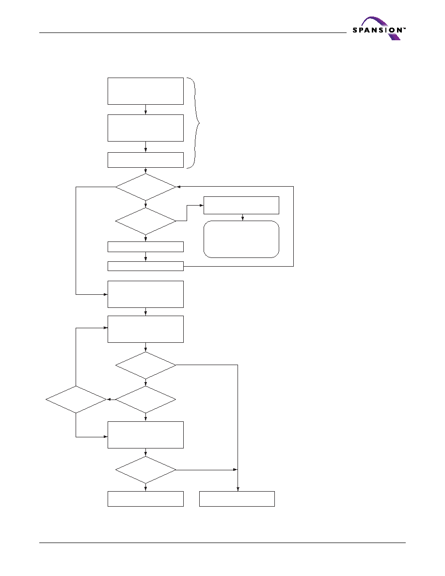
August 4, 2004 S29GLxxxM_00_B1_E
S29GLxxxM MirrorBit
TM
Flash Family
107
D a t a s h e e t
Figure 3. Write Buffer Programming Operation
Write "Write to Buffer"
command and
Sector Address
Write number of addresses
to program minus 1(WC)
and Sector Address
Write program buffer to
flash sector address
Write first address/data
Write to a different
sector address
FAIL or ABORT
PASS
Read DQ7 - DQ0 at
Last Loaded Address
Read DQ7 - DQ0 with
address = Last Loaded
Address
Write next address/data pair
WC = WC - 1
WC = 0 ?
Part of "Write to Buffer"
Command Sequence
Yes
Yes
Yes
Yes
Yes
Yes
No
No
No
No
No
No
Abort Write to
Buffer Operation?
DQ7 = Data?
DQ7 = Data?
DQ5 = 1?
DQ1 = 1?
Write to buffer ABORTED.
Must write "Write-to-buffer
Abort Reset" command
sequence to return
to read mode.
(Note 2)
(Note 3)
(Note 1)
Notes:
1. When Sector Address is specified, any address in
the selected sector is acceptable. However, when
loading Write-Buffer address locations with data, all
addresses must fall within the selected Write-Buffer
Page.
2. DQ7 may change simultaneously with DQ5.
Therefore, DQ7 should be verified.
3. If this flowchart location was reached because
DQ5= "1", then the device FAILED. If this flowchart
location was reached because DQ1= "1", then the
Write to Buffer operation was ABORTED. In either
case, the proper reset command must be written
before the device can begin another operation. If
DQ1=1, write the Write-Buffer-Programming-
Abort-Reset command. if DQ5=1, write the Reset
command.
4. See
Table
35
and Table
36
for command
sequences required for write buffer programming.
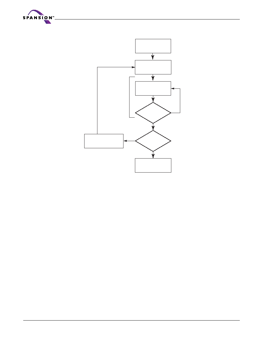
108
S29GLxxxM MirrorBit
TM
Flash Family
S29GLxxxM_00_B1_E August 4, 2004
D a t a s h e e t
Figure 4. Program Operation
Program Suspend/Program Resume Command Sequence
The Program Suspend command allows the system to interrupt a programming operation or a Write to Buffer pro-
gramming operation so that data can be read from any non-suspended sector. When the Program Suspend
command is written during a programming process, the device halts the program operation within 15 µs maximum
(5µs typical) and updates the status bits. Addresses are not required when writing the Program Suspend
command.
After the programming operation has been suspended, the system can read array data from any non-suspended
sector. The Program Suspend command may also be issued during a programming operation while an erase is
suspended. In this case, data may be read from any addresses not in Erase Suspend or Program Suspend. If a
read is needed from the SecSi Sector area (One-time Program area), then user must use the proper command
sequences to enter and exit this region. Note that the SecSi Sector, autoselect, and CFI functions are unavailable
when a program operation is in progress.
The system may also write the autoselect command sequence when the device is in the Program Suspend mode.
The system can read as many autoselect codes as required. When the device exits the autoselect mode, the device
reverts to the Program Suspend mode, and is ready for another valid operation. See Autoselect Command Se-
quence for more information.
After the Program Resume command is written, the device reverts to programming. The system can determine
the status of the program operation using the DQ7 or DQ6 status bits, just as in the standard program operation.
See Write Operation Status for more information.
START
Write Program
Command Sequence
Data Poll
from System
Verify Data?
No
Yes
Last Address?
No
Yes
Programming
Completed
Increment Address
Embedded
Program
algorithm
in progress
Note:
See Table
35
and Table
36
for program com-
mand sequence.

August 4, 2004 S29GLxxxM_00_B1_E
S29GLxxxM MirrorBit
TM
Flash Family
109
D a t a s h e e t
The system must write the Program Resume command (address bits are don't care) to exit the Program Suspend
mode and continue the programming operation. Further writes of the Resume command are ignored. Another Pro-
gram Suspend command can be written after the device has resumed programming.
Figure 5. Program Suspend/Program Resume
Chip Erase Command Sequence
Chip erase is a six bus cycle operation. The chip erase command sequence is initiated by writing two unlock cycles,
followed by a set-up command. Two additional unlock write cycles are then followed by the chip erase command,
which in turn invokes the Embedded Erase algorithm. The device does not require the system to preprogram prior
to erase. The Embedded Erase algorithm automatically preprograms and verifies the entire memory for an all zero
data pattern prior to electrical erase. The system is not required to provide any controls or timings during these
operations. Table
35
and Table
36
show the address and data requirements for the chip erase command sequence.
When the Embedded Erase algorithm is complete, the device returns to the read mode and addresses are no
longer latched. The system can determine the status of the erase operation by using DQ7, DQ6, or DQ2. Refer to
the Write Operation Status section for information on these status bits.
Any commands written during the chip erase operation are ignored. However, note that a hardware reset im-
mediately terminates the erase operation. If that occurs, the chip erase command sequence should be reinitiated
once the device has returned to reading array data, to ensure data integrity.
6 illustrates the algorithm for the erase operation. Refer to the Erase and Program Operations table in the AC
Characteristics section for parameters, and 18 section for timing diagrams.
Program Operation
or Write-to-Buffer
Sequence in Progress
Write Program Suspend
Command Sequence
Command is also valid for
Erase-suspended-program
operations
Autoselect and SecSi Sector
read operations are also allowed
Data cannot be read from erase- or
program-suspended sectors
Write Program Resume
Command Sequence
Read data as
required
Done
reading?
No
Yes
Write address/data
XXXh/30h
Device reverts to
operation prior to
Program Suspend
Write address/data
XXXh/B0h
Wait 15
µ
s

110
S29GLxxxM MirrorBit
TM
Flash Family
S29GLxxxM_00_B1_E August 4, 2004
D a t a s h e e t
Sector Erase Command Sequence
Sector erase is a six bus cycle operation. The sector erase command sequence is initiated by writing two unlock
cycles, followed by a set-up command. Two additional unlock cycles are written, and are then followed by the
address of the sector to be erased, and the sector erase command. Table
35
and Table
36
shows the address and
data requirements for the sector erase command sequence.
The device does not require the system to preprogram prior to erase. The Embedded Erase algorithm automati-
cally programs and verifies the entire memory for an all zero data pattern prior to electrical erase. The system is
not required to provide any controls or timings during these operations.
After the command sequence is written, a sector erase time-out of 50 µs occurs. During the time-out period, ad-
ditional sector addresses and sector erase commands may be written. Loading the sector erase buffer may be
done in any sequence, and the number of sectors may be from one sector to all sectors. The time between these
additional cycles must be less than 50 µs, otherwise erasure may begin. Any sector erase address and command
following the exceeded time-out may or may not be accepted. It is recommended that processor interrupts be
disabled during this time to ensure all commands are accepted. The interrupts can be re-enabled after the last
Sector Erase command is written. Any command other than Sector Erase or Erase Suspend during the
time-out period resets the device to the read mode. Note that the SecSi Sector, autoselect, and CFI func-
tions are unavailable when an erase operation is in progress. The system must rewrite the command sequence
and any additional addresses and commands.
The system can monitor DQ3 to determine if the sector erase timer has timed out (See the section on DQ3: Sector
Erase Timer.). The time-out begins from the rising edge of the final WE# pulse in the command sequence.
When the Embedded Erase algorithm is complete, the device returns to reading array data and addresses are no
longer latched. The system can determine the status of the erase operation by reading DQ7, DQ6, or DQ2 in the
erasing sector. Refer to the Write Operation Status section for information on these status bits.
Once the sector erase operation has begun, only the Erase Suspend command is valid. All other commands are
ignored. However, note that a hardware reset immediately terminates the erase operation. If that occurs, the
sector erase command sequence should be reinitiated once the device has returned to reading array data, to en-
sure data integrity.
6 illustrates the algorithm for the erase operation. Refer to the Erase and Program Operations table in the AC
Characteristics section for parameters, and 18 section for timing diagrams.
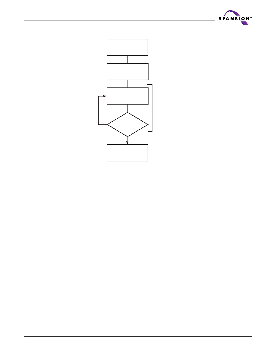
August 4, 2004 S29GLxxxM_00_B1_E
S29GLxxxM MirrorBit
TM
Flash Family
111
D a t a s h e e t
Figure 6. Erase Operation
Erase Suspend/Erase Resume Commands
The Erase Suspend command, B0h, allows the system to interrupt a sector erase operation and then read data
from, or program data to, any sector not selected for erasure. This command is valid only during the sector erase
operation, including the 50 µs time-out period during the sector erase command sequence. The Erase Suspend
command is ignored if written during the chip erase operation or Embedded Program algorithm.
When the Erase Suspend command is written during the sector erase operation, the device requires a typical of
5 µs
(maximum of 20 µs) to suspend the erase operation. However, when the Erase Suspend command is written
during the sector erase time-out, the device immediately terminates the time-out period and suspends the erase
operation.
After the erase operation has been suspended, the device enters the erase-suspend-read mode. The system can
read data from or program data to any sector not selected for erasure. (The device "erase suspends" all sectors
selected for erasure.) Reading at any address within erase-suspended sectors produces status information on
DQ7≠DQ0. The system can use DQ7, or DQ6 and DQ2 together, to determine if a sector is actively erasing or is
erase-suspended. Refer to the Write Operation Status section for information on these status bits.
After an erase-suspended program operation is complete, the device returns to the erase-suspend-read mode.
The system can determine the status of the program operation using the DQ7 or DQ6 status bits, just as in the
standard word program operation. Refer to the Write Operation Status section for more information.
In the erase-suspend-read mode, the system can also issue the autoselect command sequence. Refer to the "Au-
toselect Mode" section on page 79 and "Autoselect Command Sequence" section on page 104 sections for details.
START
Write Erase
Command Sequence
(Notes 1, 2)
Data Poll to Erasing
Bank from System
Data = FFh?
No
Yes
Erasure Completed
Embedded
Erase
algorithm
in progress
Notes:
1. See Table
35
and Table
36
for program command
sequence.
2. See the section on DQ3 for information on the sector
erase timer.

112
S29GLxxxM MirrorBit
TM
Flash Family
S29GLxxxM_00_B1_E August 4, 2004
D a t a s h e e t
To resume the sector erase operation, the system must write the Erase Resume command. Further writes of the
Resume command are ignored. Another Erase Suspend command can be written after the chip has resumed
erasing.
Note: During an erase operation, this flash device performs multiple internal operations which are invisible to the
system. When an erase operation is suspended, any of the internal operations that were not fully completed must
be restarted. As such, if this flash device is continually issued suspend/resume commands in rapid succession,
erase progress will be impeded as a function of the number of suspends. The result will be a longer cumulative
erase time than without suspends. Note that the additional suspends do not affect device reliability or future per-
formance. In most systems rapid erase/suspend activity occurs only briefly. In such cases, erase performance will
not be significantly impacted.

August 4, 2004 S29GLxxxM_00_B1_E
S29GLxxxM MirrorBit
TM
Flash Family
113
D a t a s h e e t
Command Definitions
Table 35. Command Definitions (x16 Mode, BYTE# = V
IH
)
Command
Sequence
(Note 1)
Cyc
l
e
s
Bus Cycles (Notes 2≠5)
First
Second
Third
Fourth
Fifth
Sixth
Addr Data
Addr
Data
Addr
Data
Addr
Data
Addr
Data Addr Data
Read (Note 6)
1
RA
RD
Reset (Note 7)
1
XXX
F0
Au
t
o
s
e
l
e
c
t
(
N
o
t
e
8
)
Manufacturer ID
4
555
AA
2AA
55
555
90
X00
0001
Device ID (Note 9)
4
555
AA
2AA
55
555
90
X01
227E
X0E
(Note
18)
X0F
(Note
18)
SecSi Sector Factory Protect
(Note 10)
4
555
AA
2AA
55
555
90
X03
(Note 10)
Sector Group Protect Verify (Note
12)
4
555
AA
2AA
55
555
90
(SA)X02
00/01
Enter SecSi Sector Region
3
555
AA
2AA
55
555
88
Exit SecSi Sector Region
4
555
AA
2AA
55
555
90
XXX
00
Program
4
555
AA
2AA
55
555
A0
PA
PD
Write to Buffer (Note 11)
3
555
AA
2AA
55
SA
25
SA
WC
PA
PD
WBL
PD
Program Buffer to Flash
1
SA
29
Write to Buffer Abort Reset (Note 13)
3
555
AA
2AA
55
555
F0
Unlock Bypass
3
555
AA
2AA
55
555
20
Unlock Bypass Program (Note 14)
2
XXX
A0
PA
PD
Unlock Bypass Reset (Note 15)
2
XXX
90
XXX
00
Chip Erase
6
555
AA
2AA
55
555
80
555
AA
2AA
55
555
10
Sector Erase
6
555
AA
2AA
55
555
80
555
AA
2AA
55
SA
30
Program/Erase Suspend (Note 16)
1
XXX
B0
Program/Erase Resume (Note 17)
1
XXX
30
CFI Query (Note 18)
1
55
98
Legend:
X = Don't care
RA = Read Address of memory location to be read.
RD = Read Data read from location RA during read operation.
PA = Program Address. Addresses latch on falling edge of WE# or
CE# pulse, whichever happens later.
PD = Program Data for location PA. Data latches on rising edge of
WE# or CE# pulse, whichever happens first.
SA = Sector Address of sector to be verified (in autoselect mode) or
erased. Address bits A21≠A15 uniquely select any sector.
WBL = Write Buffer Location. Address must be within same write
buffer page as PA.
WC = Word Count. Number of write buffer locations to load minus 1.
Notes:
1. See
Table 1
for description of bus operations.
2. All values are in hexadecimal.
3. Shaded cells indicate read cycles. All others are write cycles.
4. During unlock and command cycles, when lower address bits are
555 or 2AA as shown in table, address bits above A11 and data
bits above DQ7 are don't care.
5. No unlock or command cycles required when device is in read
mode.
6. Reset command is required to return to read mode (or to erase-
suspend-read mode if previously in Erase Suspend) when device
is in autoselect mode, or if DQ5 goes high while device is
providing status information.
7. Fourth cycle of the autoselect command sequence is a read
cycle. Data bits DQ15≠DQ8 are don't care. Except for RD, PD
and WC. See
Autoselect Command Sequence
section for more
information.
8. Device ID must be read in three cycles.
9. If WP# protects highest address sector, data is 98h for factory
locked and 18h for not factory locked. If WP# protects lowest
address sector, data is 88h for factory locked and 08h for not
factor locked.
10. Data is 00h for an unprotected sector group and 01h for a
protected sector group.
11. Total number of cycles in command sequence is determined by
number of words written to write buffer. Maximum number of
cycles in command sequence is 21, including "Program Buffer to
Flash" command.
12. Command sequence resets device for next command after
aborted write-to-buffer operation.
13. Unlock Bypass command is required prior to Unlock Bypass
Program command.
14. Unlock Bypass Reset command is required to return to read
mode when device is in unlock bypass mode.
15. System may read and program in non-erasing sectors, or enter
autoselect mode, when in Erase Suspend mode. Erase Suspend
command is valid only during a sector erase operation.
16. Erase Resume command is valid only during Erase Suspend
mode.
17. Command is valid when device is ready to read array data or
when device is in autoselect mode.
18. Refer to Table 18, AutoSelect Codes for individual Device IDs
per device density and model number.

114
S29GLxxxM MirrorBit
TM
Flash Family
S29GLxxxM_00_B1_E August 4, 2004
D a t a s h e e t
Table 36. Command Definitions (x8 Mode, BYTE# = V
IL
)
Command
Sequence
(Note 1)
Cyc
l
e
s
Bus Cycles (Notes 2≠5)
First
Second
Third
Fourth
Fifth
Sixth
Addr Data
Addr
Data
Addr
Data
Addr
Data
Addr
Data Addr Data
Read (Note 6)
1
RA
RD
Reset (Note 7)
1
XXX
F0
Au
t
o
s
e
l
e
c
t
(
N
o
t
e
8
)
Manufacturer ID
4
AAA
AA
555
55
AAA
90
X00
01
Device ID (Note 9)
4
AAA
AA
555
55
AAA
90
X02
7E
X1C
(Note
17)
X1E
(Note
17)
SecSi Sector Factory
Protect (Note 10)
4
AAA
AA
555
55
AAA
90
X06
(Note 10)
Sector Group Protect Verify
(Note 12)
4
AAA
AA
555
55
AAA
90
(SA)X04
00/01
Enter SecSi Sector Region
3
AAA
AA
555
55
AAA
88
Exit SecSi Sector Region
4
AAA
AA
555
55
AAA
90
XXX
00
Write to Buffer (Note 11)
3
AAA
AA
555
55
SA
25
SA
BC
PA
PD
WBL
PD
Program Buffer to Flash
1
SA
29
Write to Buffer Abort Reset (Note
13)
3
AAA
AA
555
55
AAA
F0
Chip Erase
6
AAA
AA
555
55
AAA
80
AAA
AA
555
55
AAA
10
Sector Erase
6
AAA
AA
555
55
AAA
80
AAA
AA
555
55
SA
30
Program/Erase Suspend (Note
14)
1
XXX
B0
Program/Erase Resume (Note
15)
1
XXX
30
CFI Query (Note 16)
1
AA
98
Legend:
X = Don't care
RA = Read Address of memory location to be read.
RD = Read Data read from location RA during read operation.
PA = Program Address. Addresses latch on falling edge of WE# or
CE# pulse, whichever happens later.
PD = Program Data for location PA. Data latches on rising edge of
WE# or CE# pulse, whichever happens first.
SA = Sector Address of sector to be verified (in autoselect mode) or
erased. Address bits A21≠A15 uniquely select any sector.
WBL = Write Buffer Location. Address must be within same write
buffer page as PA.
BC = Byte Count. Number of write buffer locations to load minus 1.
Notes:
1. See
Table 1
for description of bus operations.
2. All values are in hexadecimal.
3. Shaded cells indicate read cycles. All others are write cycles.
4. During unlock and command cycles, when lower address bits are
555 or AAA as shown in table, address bits above A11 are don't
care.
5. Unless otherwise noted, address bits A21≠A11 are don't cares.
6. No unlock or command cycles required when device is in read
mode.
7. Reset command is required to return to read mode (or to erase-
suspend-read mode if previously in Erase Suspend) when device
is in autoselect mode, or if DQ5 goes high while device is
providing status information.
8. Fourth cycle of autoselect command sequence is a read cycle.
Data bits DQ15≠DQ8 are don't care. See
Autoselect Command
Sequence
section or more information.
9. Device ID must be read in three cycles.
10. If WP# protects highest address sector, data is 98h for factory
locked and 18h for not factory locked. If WP# protects lowest
address sector, data is 88h for factory locked and 08h for not
factor locked.
11. Data is 00h for an unprotected sector group and 01h for a
protected sector group.
12. Total number of cycles in command sequence is determined by
number of bytes written to write buffer. Maximum number of
cycles in command sequence is 37, including "Program Buffer to
Flash" command.
13. Command sequence resets device for next command after
aborted write-to-buffer operation.
14. System may read and program in non-erasing sectors, or enter
autoselect mode, when in Erase Suspend mode. Erase Suspend
command is valid only during a sector erase operation.
15. Erase Resume command is valid only during Erase Suspend
mode.
16. Command is valid when device is ready to read array data or
when device is in autoselect mode.
17. Refer to Table 18, AutoSelect Codes for individual Device IDs
per device density and model number.

August 4, 2004 S29GLxxxM_00_B1_E
S29GLxxxM MirrorBit
TM
Flash Family
115
D a t a s h e e t
Write Operation Status
The device provides several bits to determine the status of a program or erase operation: DQ2, DQ3, DQ5, DQ6,
and DQ7. Table 19 and the following subsections describe the function of these bits. DQ7 and DQ6 each offer a
method for determining whether a program or erase operation is complete or in progress. The device also pro-
vides a hardware-based output signal, RY/BY#, to determine whether an Embedded Program or Erase operation
is in progress or has been completed.
DQ7: Data# Polling
The Data# Polling bit, DQ7, indicates to the host system whether an Embedded Program or Erase algorithm is in
progress or completed, or whether the device is in Erase Suspend. Data# Polling is valid after the rising edge of
the final WE# pulse in the command sequence.
During the Embedded Program algorithm, the device outputs on DQ7 the complement of the datum programmed
to DQ7. This DQ7 status also applies to programming during Erase Suspend. When the Embedded Program algo-
rithm is complete, the device outputs the datum programmed to DQ7. The system must provide the program
address to read valid status information on DQ7. If a program address falls within a protected sector, Data# Polling
on DQ7 is active for approximately 1 µs, then the device returns to the read mode.
During the Embedded Erase algorithm, Data# Polling produces a "0" on DQ7. When the Embedded Erase algo-
rithm is complete, or if the device enters the Erase Suspend mode, Data# Polling produces a "1" on DQ7. The
system must provide an address within any of the sectors selected for erasure to read valid status information on
DQ7.
After an erase command sequence is written, if all sectors selected for erasing are protected, Data# Polling on
DQ7 is active for approximately 100 µs, then the device returns to the read mode. If not all selected sectors are
protected, the Embedded Erase algorithm erases the unprotected sectors, and ignores the selected sectors that
are protected. However, if the system reads DQ7 at an address within a protected sector, the status may not be
valid.
Just prior to the completion of an Embedded Program or Erase operation, DQ7 may change asynchronously with
DQ0≠DQ6 while Output Enable (OE#) is asserted low. That is, the device may change from providing status in-
formation to valid data on DQ7. Depending on when the system samples the DQ7 output, it may read the status
or valid data. Even if the device has completed the program or erase operation and DQ7 has valid data, the data
outputs on DQ0≠DQ6 may be still invalid. Valid data on DQ0≠DQ7 will appear on successive read cycles.
Table
37
shows the outputs for Data# Polling on DQ7. Figure 7 shows the Data# Polling algorithm. Figure 17 in
the AC Characteristics section shows the Data# Polling timing diagram.
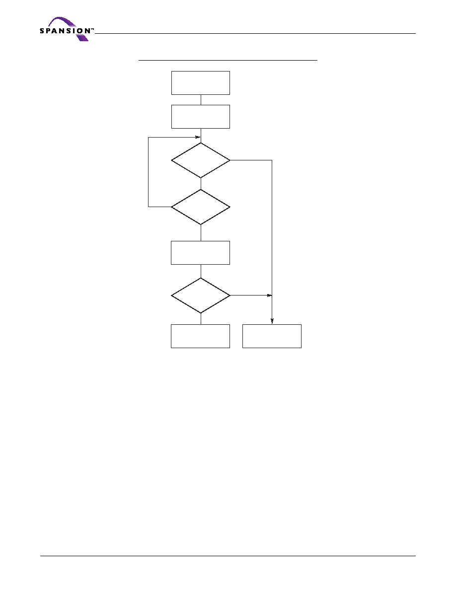
116
S29GLxxxM MirrorBit
TM
Flash Family
S29GLxxxM_00_B1_E August 4, 2004
D a t a s h e e t
Figure 7. Data# Polling Algorithm
RY/BY#: Ready/Busy#
The RY/BY# is a dedicated, open-drain output pin which indicates whether an Embedded Algorithm is in progress
or complete. The RY/BY# status is valid after the rising edge of the final WE# pulse in the command sequence.
Since RY/BY# is an open-drain output, several RY/BY# pins can be tied together in parallel with a pull-up resistor
to V
CC
.
If the output is low (Busy), the device is actively erasing or programming. (This includes programming in the Erase
Suspend mode.) If the output is high (Ready), the device is in the read mode, the standby mode, or in the erase-
suspend-read mode. Table
37
shows the outputs for RY/BY#.
DQ7 = Data?
Yes
No
No
DQ5 = 1?
No
Yes
Yes
FAIL
PASS
Read DQ15≠DQ0
Addr = VA
Read DQ15≠DQ0
Addr = VA
DQ7 = Data?
START
Notes:
1. VA = Valid address for programming. During a sector
erase operation, a valid address is any sector address
within the sector being erased. During chip erase, a
valid address is any non-protected sector address.
2. DQ7 should be rechecked even if DQ5 = "1" because
DQ7 may change simultaneously with DQ5.

August 4, 2004 S29GLxxxM_00_B1_E
S29GLxxxM MirrorBit
TM
Flash Family
117
D a t a s h e e t
DQ6: Toggle Bit I
Toggle Bit I on DQ6 indicates whether an Embedded Program or Erase algorithm is in progress or complete, or
whether the device has entered the Erase Suspend mode. Toggle Bit I may be read at any address, and is valid
after the rising edge of the final WE# pulse in the command sequence (prior to the program or erase operation),
and during the sector erase time-out.
During an Embedded Program or Erase algorithm operation, successive read cycles to any address cause DQ6 to
toggle. The system may use either OE# or CE# to control the read cycles. When the operation is complete, DQ6
stops toggling.
After an erase command sequence is written, if all sectors selected for erasing are protected, DQ6 toggles for
approximately 100 µs, then returns to reading array data. If not all selected sectors are protected, the Embedded
Erase algorithm erases the unprotected sectors, and ignores the selected sectors that are protected.
The system can use DQ6 and DQ2 together to determine whether a sector is actively erasing or is erase-sus-
pended. When the device is actively erasing (that is, the Embedded Erase algorithm is in progress), DQ6 toggles.
When the device enters the Erase Suspend mode, DQ6 stops toggling. However, the system must also use DQ2
to determine which sectors are erasing or erase-suspended. Alternatively, the system can use DQ7 (see the sub-
section on DQ7: Data# Polling).
If a program address falls within a protected sector, DQ6 toggles for approximately 1 µs after the program com-
mand sequence is written, then returns to reading array data.
DQ6 also toggles during the erase-suspend-program mode, and stops toggling once the Embedded Program al-
gorithm is complete.
Table
37
shows the outputs for Toggle Bit I on DQ6. Figure 8 shows the toggle bit algorithm. 20 in the "AC Char-
acteristics" section shows the toggle bit timing diagrams. 21 shows the differences between DQ2 and DQ6 in
graphical form. See also the subsection on DQ2: Toggle Bit II.

118
S29GLxxxM MirrorBit
TM
Flash Family
S29GLxxxM_00_B1_E August 4, 2004
D a t a s h e e t
Figure 8. Toggle Bit Algorithm
START
No
Yes
Yes
DQ5 = 1?
No
Yes
Toggle Bit
= Toggle?
No
Program/Erase
Operation Not
Complete, Write
Reset Command
Program/Erase
Operation Complete
Read DQ7≠DQ0
Toggle Bit
= Toggle?
Read DQ7≠DQ0
Twice
Read DQ7≠DQ0
N o t e :
The system should recheck the toggle bit even if DQ5 = "1"
because the toggle bit may stop toggling as DQ5 changes
to "1." See the subsections on DQ6 and DQ2 for more
information.

August 4, 2004 S29GLxxxM_00_B1_E
S29GLxxxM MirrorBit
TM
Flash Family
119
D a t a s h e e t
DQ2: Toggle Bit II
The "Toggle Bit II" on DQ2, when used with DQ6, indicates whether a particular sector is actively erasing (that is,
the Embedded Erase algorithm is in progress), or whether that sector is erase-suspended. Toggle Bit II is valid
after the rising edge of the final WE# pulse in the command sequence.
DQ2 toggles when the system reads at addresses within those sectors that have been selected for erasure. (The
system may use either OE# or CE# to control the read cycles.) But DQ2 cannot distinguish whether the sector is
actively erasing or is erase-suspended. DQ6, by comparison, indicates whether the device is actively erasing, or
is in Erase Suspend, but cannot distinguish which sectors are selected for erasure. Thus, both status bits are re-
quired for sector and mode information. Refer to Table
37
to compare outputs for DQ2 and DQ6.
8 shows the toggle bit algorithm in flowchart form, and the section "DQ2: Toggle Bit II" explains the algorithm.
See also the RY/BY#: Ready/Busy# subsection. 20 shows the toggle bit timing diagram. 21 shows the differences
between DQ2 and DQ6 in graphical form.
Reading Toggle Bits DQ6/DQ2
Refer to 8 for the following discussion. Whenever the system initially begins reading toggle bit status, it must
read DQ7≠DQ0 at least twice in a row to determine whether a toggle bit is toggling. Typically, the system would
note and store the value of the toggle bit after the first read. After the second read, the system would compare
the new value of the toggle bit with the first. If the toggle bit is not toggling, the device has completed the program
or erase operation. The system can read array data on DQ7≠DQ0 on the following read cycle.
However, if after the initial two read cycles, the system determines that the toggle bit is still toggling, the system
also should note whether the value of DQ5 is high (see the section on DQ5). If it is, the system should then de-
termine again whether the toggle bit is toggling, since the toggle bit may have stopped toggling just as DQ5 went
high. If the toggle bit is no longer toggling, the device has successfully completed the program or erase operation.
If it is still toggling, the device did not completed the operation successfully, and the system must write the reset
command to return to reading array data.
The remaining scenario is that the system initially determines that the toggle bit is toggling and DQ5 has not gone
high. The system may continue to monitor the toggle bit and DQ5 through successive read cycles, determining
the status as described in the previous paragraph. Alternatively, it may choose to perform other system tasks. In
this case, the system must start at the beginning of the algorithm when it returns to determine the status of the
operation (top of Figure 6).
DQ5: Exceeded Timing Limits
DQ5 indicates whether the program, erase, or write-to-buffer time has exceeded a specified internal pulse count
limit. Under these conditions DQ5 produces a "1," indicating that the program or erase cycle was not successfully
completed.
The device may output a "1" on DQ5 if the system tries to program a "1" to a location that was previously pro-
grammed to "0." Only an erase operation can change a "0" back to a "1." Under this condition, the device
halts the operation, and when the timing limit has been exceeded, DQ5 produces a "1."
In all these cases, the system must write the reset command to return the device to the reading the array (or to
erase-suspend-read if the device was previously in the erase-suspend-program mode).
DQ3: Sector Erase Timer
After writing a sector erase command sequence, the system may read DQ3 to determine whether or not erasure
has begun. (The sector erase timer does not apply to the chip erase command.) If additional sectors are selected
for erasure, the entire time-out also applies after each additional sector erase command. When the time-out pe-
riod is complete, DQ3 switches from a "0" to a "1." If the time between additional sector erase commands from
the system can be assumed to be less than 50 µs, the system need not monitor DQ3. See also the Sector Erase
Command Sequence section.

120
S29GLxxxM MirrorBit
TM
Flash Family
S29GLxxxM_00_B1_E August 4, 2004
D a t a s h e e t
After the sector erase command is written, the system should read the status of DQ7 (Data# Polling) or DQ6 (Tog-
gle Bit I) to ensure that the device has accepted the command sequence, and then read DQ3. If DQ3 is "1," the
Embedded Erase algorithm has begun; all further commands (except Erase Suspend) are ignored until the erase
operation is complete. If DQ3 is "0," the device will accept additional sector erase commands. To ensure the com-
mand has been accepted, the system software should check the status of DQ3 prior to and following each
subsequent sector erase command. If DQ3 is high on the second status check, the last command might not have
been accepted.
Table
37
shows the status of DQ3 relative to the other status bits.
DQ1: Write-to-Buffer Abort
DQ1 indicates whether a Write-to-Buffer operation was aborted. Under these conditions DQ1 produces a "1". The
system must issue the Write-to-Buffer-Abort-Reset command sequence to return the device to reading array data.
See Write Buffer section for more details.
Table 37. Write Operation Status
Notes:
1. DQ5 switches to `1' when an Embedded Program, Embedded Erase, or Write-to-Buffer operation has exceeded the
maximum timing limits. Refer to the section on DQ5 for more information.
2. DQ7 and DQ2 require a valid address when reading status information. Refer to the appropriate subsection for
further details.
3. The Data# Polling algorithm should be used to monitor the last loaded write-buffer address location.
4. DQ1 switches to `1' when the device has aborted the write-to-buffer operation
Status
DQ7
(Note 2)
DQ6
DQ5
(Note 1)
DQ3
DQ2
(Note 2)
DQ1
RY/
BY#
Standard
Mode
Embedded Program Algorithm
DQ7#
Toggle
0
N/A
No toggle
0
0
Embedded Erase Algorithm
0
Toggle
0
1
Toggle
N/A
0
Program
Suspend
Mode
Program-
Suspend
Read
Program-Suspended
Sector
Invalid (not allowed)
1
Non-Program
Suspended Sector
Data
1
Erase
Suspend
Mode
Erase-
Suspend
Read
Erase-Suspended
Sector
1
No toggle
0
N/A
Toggle
N/A
1
Non-Erase
Suspended Sector
Data
1
Erase-Suspend-Program
(Embedded Program)
DQ7#
Toggle
0
N/A
N/A
N/A
0
Write-to-
Buffer
Busy (Note 3)
DQ7#
Toggle
0
N/A
N/A
0
0
Abort (Note 4)
DQ7#
Toggle
0
N/A
N/A
1
0

August 4, 2004 S29GLxxxM_00_B1_E
S29GLxxxM MirrorBit
TM
Flash Family
121
D a t a s h e e t
Absolute Maximum Ratings
Storage Temperature, Plastic Packages. . . . . . . . . . . . . . . . ≠65∞C to +150∞C
Ambient Temperature with Power Applied . . . . . . . . . . . . . . ≠65∞C to +125∞C
Voltage with Respect to Ground:
V
CC
(Note 1). . . . . . . . . . . . . . . . . . . . . . . . . . . . . . .≠0.5 V to +4.0 V
. . . . . . . . . . . . A9, OE#, ACC and RESET# (Note 2)≠0.5 V to +12.5 V
All other pins (Note 1) . . . . . . . . . . . . . . . . . . . . . ≠0.5 V to V
CC
+0.5 V
Output Short Circuit Current (Note 3). . . . . . . . . . . . . . . . . . . . . . . . 200 mA
Notes:
1. Minimum DC voltage on input or I/Os is ≠0.5 V. During voltage transitions, inputs
or I/Os may overshoot V
SS
to ≠2.0 V for periods of up to 20 ns. See
Figure 9
.
Maximum DC voltage on input or I/Os is V
CC
+ 0.5 V. During voltage transitions,
input or I/O pins may overshoot to V
CC
+ 2.0 V for periods up to 20 ns. See
Figure
10
.
2. Minimum DC input voltage on pins A9, OE#, ACC, and RESET# is ≠0.5 V. During
voltage transitions, A9, OE#, ACC, and RESET# may overshoot V
SS
to ≠2.0 V for
periods of up to 20 ns. See
Figure 9
. Maximum DC input voltage on pin A9, OE#,
ACC, and RESET# is +12.5 V which may overshoot to +14.0V for periods up to 20
ns.
3. No more than one output may be shorted to ground at a time. Duration of the short
circuit should not be greater than one second.
4. Stresses above those listed under "Absolute Maximum Ratings" may cause
permanent damage to the device. This is a stress rating only; functional operation
of the device at these or any other conditions above those indicated in the
operational sections of this data sheet is not implied. Exposure of the device to
absolute maximum rating conditions for extended periods may affect device
reliability.
Operating Ranges
Industrial (I) Devices
Ambient Temperature (T
A
) . . . . . . . . . . . . . . . . . . . . . . . . . ≠40∞C to +85∞C
Supply Voltages
V
CC
for full voltage range . . . . . . . . . . . . . . . . . . . . . . . . . +2.7 V to +3.6 V
V
CC
for regulated voltage range . . . . . . . . . . . . . . . . . . . . . +3.0 V to +3.6 V
V
IO
. . . . . . . . . . . . . . . . . . . . . . . . . . . . . . . . . . . . . . . . . . . . . . . . V
CC
Notes:
1. Operating ranges define those limits between which the functionality of the device is guaranteed.
Figure 9. Maximum Negative
Overshoot Waveform
Figure 10. Maximum Positive
Overshoot Waveform
20 ns
20 ns
+0.8 V
≠0.5 V
20 ns
≠2.0 V
20 ns
20 ns
V
CC
+2.0 V
V
CC
+0.5 V
20 ns
2.0 V

122
S29GLxxxM MirrorBit
TM
Flash Family
S29GLxxxM_00_B1_E August 4, 2004
D a t a s h e e t
DC Characteristics
CMOS Compatible
Notes:
1. On the WP#/ACC pin only, the maximum input load current when WP# = V
IL
is ± 2.0 µA.
2. The I
CC
current listed is typically less than 2 mA/MHz, with OE# at V
IH
.
3. Maximum I
CC
specifications are tested with V
CC
= V
CC
max.
4. S29GL032M, S29GL064M
5. S29GL128M, S29GL256M
6. I
CC
active while Embedded Erase or Embedded Program is in progress.
7. Automatic sleep mode enables the low power mode when addresses remain stable for t
ACC
+ 30 ns.
8. V
CC
voltage requirements.
9. Not 100% tested.
Parameter
Symbol
Parameter Description
(Notes)
Test Conditions
Min
Typ
Max
Unit
I
LI
Input Load Current (1)
V
IN
= V
SS
to V
CC
,
V
CC
= V
CC
max
±1.0
µA
I
LIT
A9, ACC Input Load Current
V
CC
= V
CC max
; A9 = 12.5 V
35
µA
I
LR
Reset Leakage Current
V
CC
= V
CC max
; RESET# = 12.5 V
35
µA
I
LO
Output Leakage Current
V
OUT
= V
SS
to V
CC
,
V
CC
= V
CC max
±1.0
µA
I
CC1
V
CC
Initial Read Current (2), (3)
CE# = V
IL,
OE# = V
IH
,
1 MHz
5
20
mA
5 MHz (4)
18
25
5 MHz (5)
25
35
10 MHz (4)
35
50
10 MHz (5)
40
60
I
CC2
V
CC
Intra-Page Read Current (2), (3)
CE# = V
IL,
OE# = V
IH
10 MHz
5
20
mA
40 MHz
10
40
I
CC3
V
CC
Active Write Current (3), (4)
CE# = V
IL,
OE# = V
IH
50
60
mA
I
CC4
V
CC
Standby Current (3)
CE#, RESET# = V
CC
± 0.3 V,
WP# = V
IH
1
5
µA
I
CC5
V
CC
Reset Current (3)
RESET# = V
SS
± 0.3 V, WP# = V
IH
1
5
µA
I
CC6
Automatic Sleep Mode (3), (7)
V
IH
= V
CC
± 0.3 V;
-0.1< V
IL
0.3 V, WP# = V
IH
1
5
µA
V
IL
Input Low Voltage 1(8)
≠0.5
0.8
V
V
IH
Input High Voltage 1 (8)
0.7 V
CC
V
CC
+ 0.5
V
V
HH
Voltage for ACC Program Acceleration
V
CC
= 2.7 ≠3.6 V
11.5
12.0
12.5
V
V
ID
Voltage for Autoselect and Temporary
Sector Unprotect
V
CC
= 2.7 ≠3.6 V
11.5
12.0
12.5
V
V
OL
Output Low Voltage (8)
I
OL
= 4.0 mA, V
CC
= V
CC min
0.45
V
V
OH1
Output High Voltage
I
OH
= ≠2.0 mA, V
CC
= V
CC min
0.85
V
CC
V
V
OH2
I
OH
= ≠100 µA, V
CC
= V
CC min
V
CC
≠0.4
V
V
LKO
Low V
CC
Lock-Out Voltage (9)
2.3
2.5
V
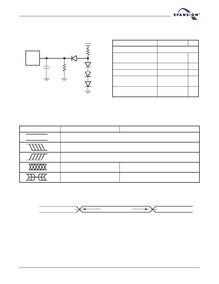
August 4, 2004 S29GLxxxM_00_B1_E
S29GLxxxM MirrorBit
TM
Flash Family
123
D a t a s h e e t
Test Conditions
Key to Switching Waveforms
Figure 12. Input Waveforms and
Measurement Levels
Note: Diodes are IN3064 or equivalent
Figure 11. Test Setup
Table 38. Test Specifications
2.7 k
CL
6.2 k
3.3 V
Device
Under
Test
Test Condition
All Speeds
Unit
Output Load
1 TTL gate
Output Load Capacitance, C
L
(including jig capacitance)
30
pF
Input Rise and Fall Times
5
ns
Input Pulse Levels
0.0 or V
CC
V
Input timing measurement
reference levels (See Note)
0.5 V
CC
V
Output timing measurement
reference levels
0.5 V
CC
V
WAVEFORM
INPUTS
OUTPUTS
Steady
Changing from H to L
Changing from L to H
Don't Care, Any Change Permitted
Changing, State Unknown
Does Not Apply
Center Line is High Impedance State (High Z)
VCC
0.0 V
Output
Measurement Level
Input
0.5 VCC
0.5 VCC
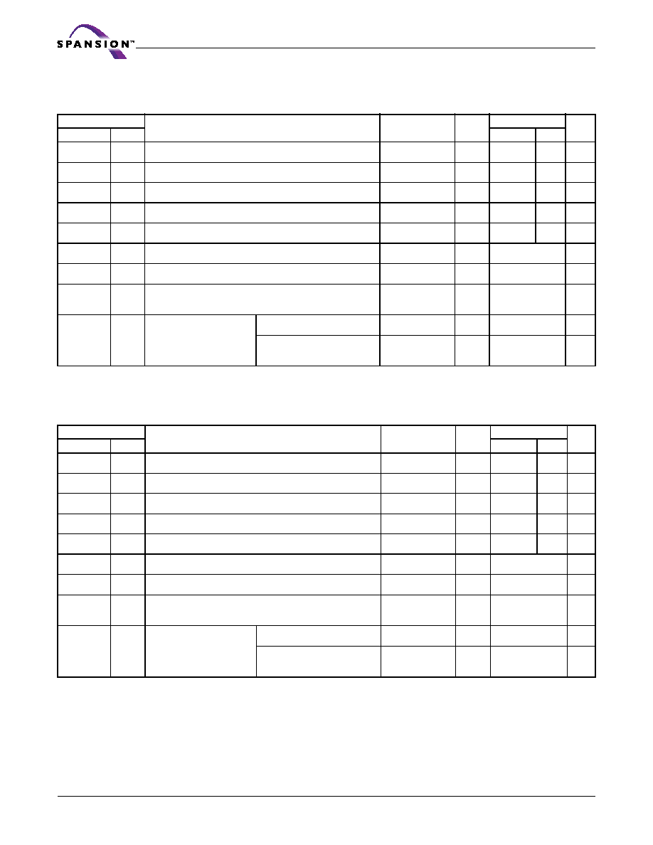
124
S29GLxxxM MirrorBit
TM
Flash Family
S29GLxxxM_00_B1_E August 4, 2004
D a t a s h e e t
AC Characteristics
Read-Only Operations-S29GL256M only
Notes:
1. Not 100% tested.
2. See
Figure 11
and Table
38
for test specifications.
Read-Only Operations-S29GL128M only
Notes:
1. Not 100% tested.
2. See
Figure 11
and Table
38
for test specifications.
Parameter
Description
Test Setup
Speed Options
Unit
JEDEC
Std.
10
11
t
AVAV
t
RC
Read Cycle Time (Note 1)
Min
100
100
ns
t
AVQV
t
ACC
Address to Output Delay
CE#, OE# = V
IL
Max
100
100
ns
t
ELQV
t
CE
Chip Enable to Output Delay
OE# = V
IL
Max
100
100
ns
t
PACC
Page Access Time
Max
30
30
ns
t
GLQV
t
OE
Output Enable to Output Delay
Max
30
30
ns
t
EHQZ
t
DF
Chip Enable to Output High Z (Note 1)
Max
16
ns
t
GHQZ
t
DF
Output Enable to Output High Z (Note 1)
Max
16
ns
t
AXQX
t
OH
Output Hold Time From Addresses, CE# or OE#,
Whichever Occurs First
Min
0
ns
t
OEH
Output Enable Hold Time
(Note 1)
Read
Min
0
ns
Toggle and
Data# Polling
Min
10
ns
Parameter
Description
Test Setup
Speed Options
Unit
JEDEC
Std.
90
10
t
AVAV
t
RC
Read Cycle Time (Note 1)
Min
90
100
ns
t
AVQV
t
ACC
Address to Output Delay
CE#, OE# = V
IL
Max
90
100
ns
t
ELQV
t
CE
Chip Enable to Output Delay
OE# = V
IL
Max
90
100
ns
t
PACC
Page Access Time
Max
25
30
ns
t
GLQV
t
OE
Output Enable to Output Delay
Max
25
30
ns
t
EHQZ
t
DF
Chip Enable to Output High Z (Note 1)
Max
16
ns
t
GHQZ
t
DF
Output Enable to Output High Z (Note 1)
Max
16
ns
t
AXQX
t
OH
Output Hold Time From Addresses, CE# or OE#,
Whichever Occurs First
Min
0
ns
t
OEH
Output Enable Hold Time
(Note 1)
Read
Min
0
ns
Toggle and
Data# Polling
Min
10
ns
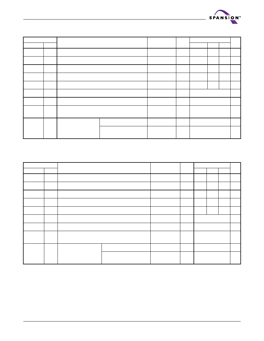
August 4, 2004 S29GLxxxM_00_B1_E
S29GLxxxM MirrorBit
TM
Flash Family
125
D a t a s h e e t
Read-Only Operations-S29GL064M only
Notes:
1. Not 100% tested.
2. See
Figure 11
and Table
38
for test specifications.
Read-Only Operations-S29GL032M only
Notes:
1. Not 100% tested.
2. See
Figure 11
and Table
38
for test specifications.
Parameter
Description
Test Setup
Speed Options
Unit
JEDEC
Std.
90
10
11
t
AVAV
t
RC
Read Cycle Time (Note 1)
Min
90
100
110
ns
t
AVQV
t
ACC
Address to Output Delay
CE#, OE# = V
IL
Max
90
100
110
ns
t
ELQV
t
CE
Chip Enable to Output Delay
OE# = V
IL
Max
90
100
110
ns
t
PACC
Page Access Time
Max
25
30
30
ns
t
GLQV
t
OE
Output Enable to Output Delay
Max
25
30
30
ns
t
EHQZ
t
DF
Chip Enable to Output High Z (Note 1)
Max
16
ns
t
GHQZ
t
DF
Output Enable to Output High Z (Note 1)
Max
16
ns
t
AXQX
t
OH
Output Hold Time From Addresses, CE# or OE#,
Whichever Occurs First
Min
0
ns
t
OEH
Output Enable Hold
Time (Note 1)
Read
Min
0
ns
Toggle and
Data# Polling
Min
10
ns
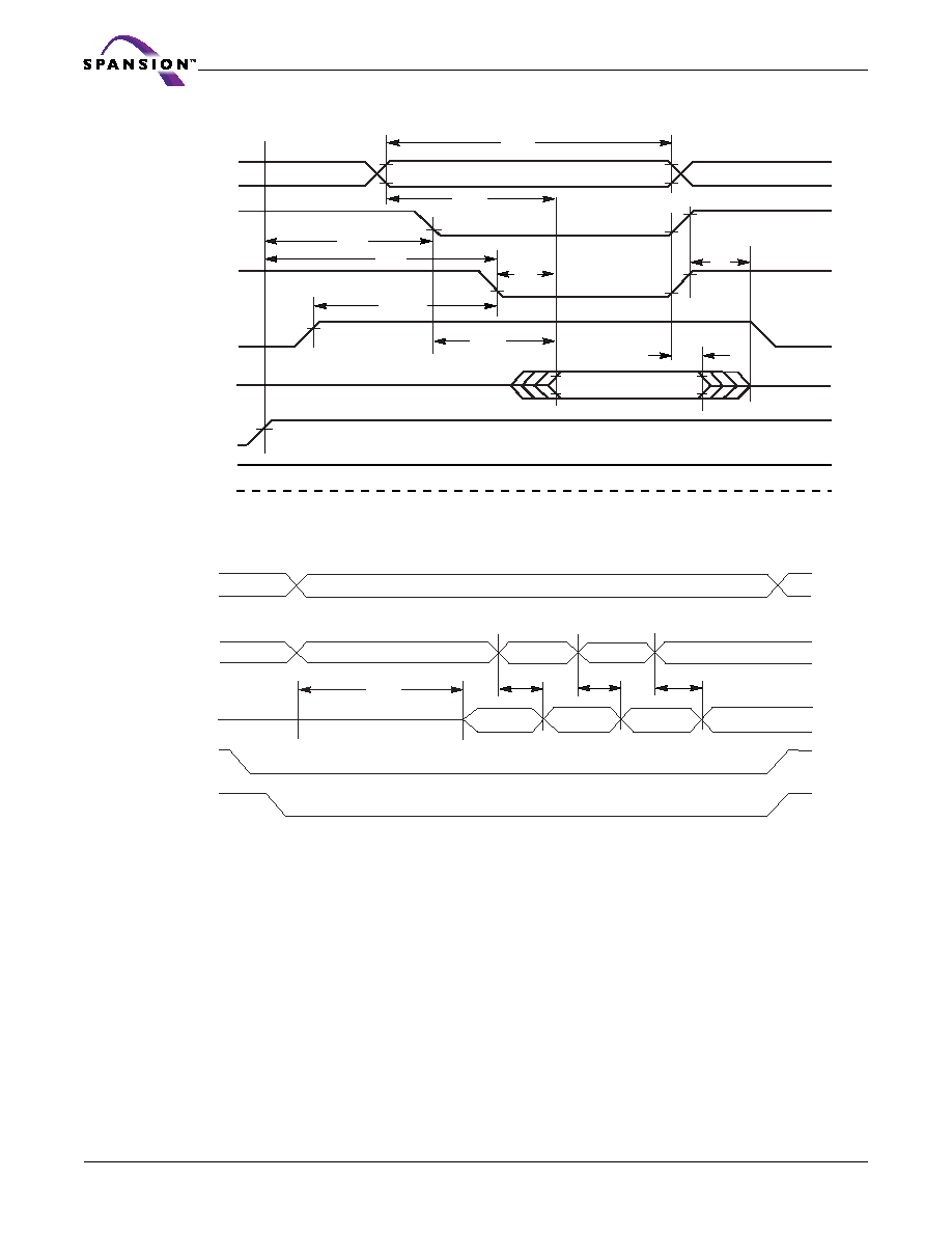
126
S29GLxxxM MirrorBit
TM
Flash Family
S29GLxxxM_00_B1_E August 4, 2004
D a t a s h e e t
Figure 13. Read Operation Timings
* Figure shows device in word mode. Addresses are A1≠A-1 for byte mode.
Figure 14. Page Read Timings
t
OH
t
CE
Outputs
WE#
Addresses
CE#
OE#
HIGH Z
Output Valid
HIGH Z
Addresses Stable
t
RC
t
ACC
t
OEH
t
RH
t
OE
t
RH
0 V
RY/BY#
RESET#
t
DF
A23-A2
CE#
OE#
A1-A0*
Data Bus
Same Page
Aa
Ab
Ac
Ad
Qa
Qb
Qc
Qd
t
ACC
t
PACC
t
PACC
t
PACC

August 4, 2004 S29GLxxxM_00_B1_E
S29GLxxxM MirrorBit
TM
Flash Family
127
D a t a s h e e t
Hardware Reset (RESET#)
Notes:
1. Not 100% tested.
Figure 15. Reset Timings
Parameter
Description
All Speed Options
Unit
JEDEC
Std.
t
Ready
RESET# Pin Low (During Embedded Algorithms)
to Read Mode (See Note)
Max
20
µs
t
Ready
RESET# Pin Low (NOT During Embedded
Algorithms) to Read Mode (See Note)
Max
500
ns
t
RP
RESET# Pulse Width
Min
500
ns
t
RH
Reset High Time Before Read (See Note)
Min
50
ns
t
RPD
RESET# Input Low to Standby Mode (See Note)
Min
20
µs
t
RB
RY/BY# Output High to CE#, OE# pin Low
Min
0
ns
RESET#
RY/BY#
RY/BY#
t
RP
t
Ready
Reset Timings NOT during Embedded Algorithms
t
Ready
CE#, OE#
t
RH
CE#, OE#
Reset Timings during Embedded Algorithms
RESET#
t
RP
t
RB
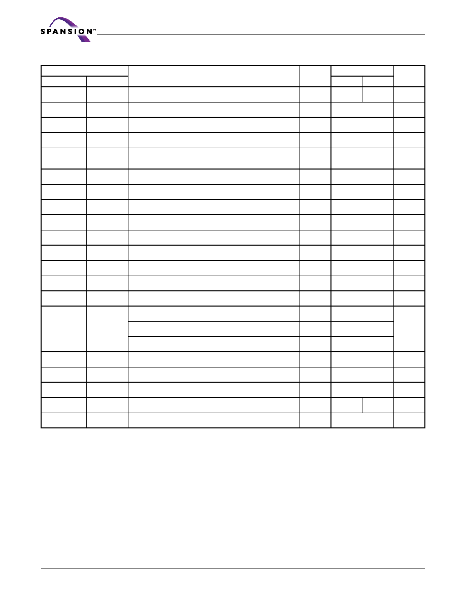
128
S29GLxxxM MirrorBit
TM
Flash Family
S29GLxxxM_00_B1_E August 4, 2004
D a t a s h e e t
Erase and Program Operations-S29GL256M only
Notes:
1. Not 100% tested.
2. See the "Erase and Programming Performance" section for more information.
3. For 1≠16 words/1≠32 bytes programmed.
4. If a program suspend command is issued within t
POLL
, the device requires t
POLL
before reading status data, once programming has resumed
(that is, the program resume command has been written). If the suspend command was issued after t
POLL
, status data is available
immediately after programming has resumed. See 16.
Parameter
Speed Options
Unit
JEDEC
Std.
Description
10
11
t
AVAV
t
WC
Write Cycle Time (Note 1)
Min
100
110
ns
t
AVWL
t
AS
Address Setup Time
Min
0
ns
t
ASO
Address Setup Time to OE# low during toggle bit polling
Min
15
ns
t
WLAX
t
AH
Address Hold Time
Min
45
ns
t
AHT
Address Hold Time From CE# or OE# high during toggle bit
polling
Min
0
ns
t
DVWH
t
DS
Data Setup Time
Min
45
ns
t
WHDX
t
DH
Data Hold Time
Min
0
ns
t
CEPH
CE# High during toggle bit polling
Min
20
ns
t
OEPH
OE# High during toggle bit polling
Min
20
ns
t
GHWL
t
GHWL
Read Recovery Time Before Write (OE# High to WE# Low)
Min
0
ns
t
ELWL
t
CS
CE# Setup Time
Min
0
ns
t
WHEH
t
CH
CE# Hold Time
Min
0
ns
t
WLWH
t
WP
Write Pulse Width
Min
35
ns
t
WHDL
t
WPH
Write Pulse Width High
Min
30
ns
t
WHWH1
t
WHWH1
Write Buffer Program Operation (Notes 2, 3)
Typ
240
µs
Single Word Program Operation (Note 2)
Typ
60
Accelerated Single Word Program Operation (Note 2)
Typ
54
t
WHWH2
t
WHWH2
Sector Erase Operation (Note 2)
Typ
0.5
sec
t
VHH
V
HH
Rise and Fall Time (Note 1)
Min
250
ns
t
VCS
V
CC
Setup Time (Note 1)
Min
50
µs
t
BUSY
WE# High to RY/BY# Low
Min
100
110
ns
t
POLL
Program Valid before Status Polling
Max
4
µs

August 4, 2004 S29GLxxxM_00_B1_E
S29GLxxxM MirrorBit
TM
Flash Family
129
D a t a s h e e t
Erase and Program Operations-S29GL128M Only
Notes:
1. Not 100% tested.
2. See the "Erase and Programming Performance" section for more information.
3. For 1≠16 words/1≠32 bytes programmed.
4. If a program suspend command is issued within t
POLL
, the device requires t
POLL
before reading status data, once programming has resumed
(that is, the program resume command has been written). If the suspend command was issued after t
POLL
, status data is available imme-
diately after programming has resumed. See 16.
Parameter
Speed Options
Unit
JEDEC
Std.
Description
90
10
t
AVAV
t
WC
Write Cycle Time (Note 1)
Min
90
100
ns
t
AVWL
t
AS
Address Setup Time
Min
0
ns
t
ASO
Address Setup Time to OE# low during toggle bit polling
Min
15
ns
t
WLAX
t
AH
Address Hold Time
Min
45
ns
t
AHT
Address Hold Time From CE# or OE# high during toggle bit
polling
Min
0
ns
t
DVWH
t
DS
Data Setup Time
Min
45
ns
t
WHDX
t
DH
Data Hold Time
Min
0
ns
t
CEPH
CE# High during toggle bit polling
Min
20
ns
t
OEPH
OE# High during toggle bit polling
Min
20
ns
t
GHWL
t
GHWL
Read Recovery Time Before Write (OE# High to WE# Low)
Min
0
ns
t
ELWL
t
CS
CE# Setup Time
Min
0
ns
t
WHEH
t
CH
CE# Hold Time
Min
0
ns
t
WLWH
t
WP
Write Pulse Width
Min
35
ns
t
WHDL
t
WPH
Write Pulse Width High
Min
30
ns
t
WHWH1
t
WHWH1
Write Buffer Program Operation (Notes 2, 3)
Typ
240
µs
Single Word Program Operation (Note 2)
Typ
60
Accelerated Single Word Program Operation (Note 2)
Typ
54
t
WHWH2
t
WHWH2
Sector Erase Operation (Note 2)
Typ
0.5
sec
t
VHH
V
HH
Rise and Fall Time (Note 1)
Min
250
ns
t
VCS
V
CC
Setup Time (Note 1)
Min
50
µs
t
BUSY
WE# High to RY/BY# Low
Min
90
100
ns
t
POLL
Program Valid before Status Polling
Max
4
µs
130
S29GLxxxM MirrorBit
TM
Flash Family
S29GLxxxM_00_B1_E August 4, 2004
D a t a s h e e t
Erase and Program Operations-S29GL064M Only
Notes:
1. Not 100% tested.
2. See the "Erase and Programming Performance" section for more information.
3. For 1≠16 words/1≠32 bytes programmed.
4. If a program suspend command is issued within t
POLL
, the device requires t
POLL
before reading status data, once programming has resumed
(that is, the program resume command has been written). If the suspend command was issued after t
POLL
, status data is available
immediately after programming has resumed. See 16.
Parameter
Speed Options
Unit
JEDEC
Std.
Description
90
10
11
t
AVAV
t
WC
Write Cycle Time (Note 1)
Min
90
100
110
ns
t
AVWL
t
AS
Address Setup Time
Min
0
ns
t
ASO
Address Setup Time to OE# low during toggle bit polling
Min
15
ns
t
WLAX
t
AH
Address Hold Time
Min
45
ns
t
AHT
Address Hold Time From CE# or OE# high during toggle bit
polling
Min
0
ns
t
DVWH
t
DS
Data Setup Time
Min
35
ns
t
WHDX
t
DH
Data Hold Time
Min
0
ns
t
CEPH
CE# High during toggle bit polling
Min
20
ns
t
OEPH
OE# High during toggle bit polling
Min
20
ns
t
GHWL
t
GHWL
Read Recovery Time Before Write (OE# High to WE# Low)
Min
0
ns
t
ELWL
t
CS
CE# Setup Time
Min
0
ns
t
WHEH
t
CH
CE# Hold Time
Min
0
ns
t
WLWH
t
WP
Write Pulse Width
Min
35
ns
t
WHDL
t
WPH
Write Pulse Width High
Min
30
ns
t
WHWH1
t
WHWH1
Write Buffer Program Operation (Notes 2, 3)
Typ
240
µs
Single Word Program Operation (Note 2)
Typ
60
Accelerated Single Word Program Operation (Note 2)
Typ
54
t
WHWH2
t
WHWH2
Sector Erase Operation (Note 2)
Typ
0.5
sec
t
VHH
V
HH
Rise and Fall Time (Note 1)
Min
250
ns
t
VCS
V
CC
Setup Time (Note 1)
Min
50
µs
t
BUSY
WE# High to RY/BY# Low
Min
90
100
110
ns
t
POLL
Program Valid before Status Polling
Max
4
µs

August 4, 2004 S29GLxxxM_00_B1_E
S29GLxxxM MirrorBit
TM
Flash Family
131
D a t a s h e e t
Erase and Program Operations-S29GL032M only
Notes:
1. Not 100% tested.
2. See the "Erase and Programming Performance" section for more information.
3. For 1≠16 words/1≠32 bytes programmed.
4. Effective write buffer specification is based upon a 16-word/32-byte write buffer operation.
5. If a program suspend command is issued within t
POLL
, the device requires t
POLL
before reading status data, once programming has resumed
(that is, the program resume command has been written). If the suspend command was issued after t
POLL
, status data is available
immediately after programming has resumed. See 16.
Notes:
1. PA = program address, PD = program data, D
OUT
is the true data at the program address.
2. Illustration shows device in word mode.
Figure 16. Program Operation Timings
Parameter
Speed Options
Unit
JEDEC
Std.
Description
90
10
11
t
AVAV
t
WC
Write Cycle Time (Note 1)
Min
90
100
110
ns
t
AVWL
t
AS
Address Setup Time
Min
0
ns
t
ASO
Address Setup Time to OE# low during toggle bit polling
Min
15
ns
t
WLAX
t
AH
Address Hold Time
Min
45
ns
t
AHT
Address Hold Time From CE# or OE# high during toggle bit
polling
Min
0
ns
t
DVWH
t
DS
Data Setup Time
Min
35
ns
t
WHDX
t
DH
Data Hold Time
Min
0
ns
t
CEPH
CE# High during toggle bit polling
Min
20
ns
t
OEPH
OE# High during toggle bit polling
Min
20
ns
t
GHWL
t
GHWL
Read Recovery Time Before Write (OE# High to WE# Low)
Min
0
ns
t
ELWL
t
CS
CE# Setup Time
Min
0
ns
t
WHEH
t
CH
CE# Hold Time
Min
0
ns
t
WLWH
t
WP
Write Pulse Width
Min
35
ns
t
WHDL
t
WPH
Write Pulse Width High
Min
30
ns
t
WHWH1
t
WHWH1
Write Buffer Program Operation (Notes 2, 3)
Typ
240
µs
Single Word Program Operation (Note 2)
Typ
60
Accelerated Single Word Program Operation (Note 2)
Typ
54
t
WHWH2
t
WHWH2
Sector Erase Operation (Note 2)
Typ
0.5
sec
t
VHH
V
HH
Rise and Fall Time (Note 1)
Min
250
ns
t
VCS
V
CC
Setup Time (Note 1)
Min
50
µs
t
BUSY
WE# High to RY/BY# Low
Min
90
100
110
ns
t
POLL
Program Valid before Status Polling
Max
4
µs

132
S29GLxxxM MirrorBit
TM
Flash Family
S29GLxxxM_00_B1_E August 4, 2004
D a t a s h e e t
Figure 17. Accelerated Program Timing Diagram
OE#
WE#
CE#
V
CC
Data
Addresses
t
DS
t
AH
t
DH
t
WP
PD
t
WHWH1
t
WC
t
AS
t
WPH
t
VCS
555h
PA
PA
Read Status Data (last two cycles)
A0h
t
POLL
t
CS
Status
D
OUT
RY/BY#
t
RB
t
BUSY
t
CH
PA
Program Command Sequence (last two cycles)
ACC
t
VHH
V
HH
V
IL
or V
IH
V
IL
or V
IH
t
VHH
ACC
t
VHH
V
HH
V
IL
or V
IH
V
IL
or V
IH
t
VHH
August 4, 2004 S29GLxxxM_00_B1_E
S29GLxxxM MirrorBit
TM
Flash Family
133
D a t a s h e e t
Notes:
1. SA = sector address (for Sector Erase), VA = Valid Address for reading status data (see "Write Operation Status".)
2. Illustration shows device in word mode.
Figure 18. Chip/Sector Erase Operation Timings
Note: VA = Valid address. Illustration shows first status cycle after command sequence, last status read cycle, and array
data read cycle.
Figure 19. Data# Polling Timings (During Embedded Algorithms)
OE#
CE#
Addresses
V
CC
WE#
Data
2AAh
SA
t
AH
t
WP
t
WC
t
AS
t
WPH
555h for chip erase
10 for Chip Erase
30h
t
DS
t
VCS
t
CS
t
DH
55h
t
CH
In
Progress
Complete
t
WHWH2
VA
VA
Erase Command Sequence (last two cycles)
Read Status Data
RY/BY#
t
RB
t
BUSY
WE#
CE#
OE#
High Z
t
OE
High Z
DQ7
DQ0≠DQ6
RY/BY#
t
BUSY
Complement
True
Addresses
VA
t
CH
VA
VA
Status Data
Complement
Status Data
True
Valid Data
Valid Data
t
POLL
t
ACC
t
CE
t
OEH
t
DF
t
OH
t
RC

134
S29GLxxxM MirrorBit
TM
Flash Family
S29GLxxxM_00_B1_E August 4, 2004
D a t a s h e e t
Note: VA = Valid address; not required for DQ6. Illustration shows first two status cycle after command sequence, last
status read cycle, and array data read cycle.
Figure 20. Toggle Bit Timings (During Embedded Algorithms)
Note: DQ2 toggles only when read at an address within an erase-suspended sector. The system may use OE# or CE#
to toggle DQ2 and DQ6.
Figure 21. DQ2 vs. DQ6
Temporary Sector Unprotect
Note:Not 100% tested.
Parameter
All Speed Options
JEDEC
Std
Description
Unit
t
VIDR
V
ID
Rise and Fall Time (See Note)
Min
500
ns
t
RSP
RESET# Setup Time for Temporary Sector
Unprotect
Min
4
µs
OE#
CE#
WE#
Addresses
t
OEH
t
DH
t
AHT
t
ASO
t
OEPH
t
OE
Valid Data
(first read)
(second read)
(stops toggling)
t
CEPH
t
AHT
t
AS
DQ6 / DQ2
Valid Data
Valid
Status
Valid
Status
Valid
Status
RY/BY#
Enter
Erase
Erase
Erase
Enter Erase
Suspend Program
Erase Suspend
Read
Erase Suspend
Read
Erase
WE#
DQ6
DQ2
Erase
Complete
Erase
Suspend
Suspend
Program
Resume
Embedded
Erasing
August 4, 2004 S29GLxxxM_00_B1_E
S29GLxxxM MirrorBit
TM
Flash Family
135
D a t a s h e e t
Figure 22. Temporary Sector Group Unprotect Timing Diagram
Note: For sector group protect, A6:A0 = 0xx0010. For sector group unprotect, A6:A0 = 1xx0010.
Figure 23. Sector Group Protect and Unprotect Timing Diagram
RESET#
t
VIDR
V
ID
V
SS
, V
IL
,
or V
IH
V
ID
V
SS
, V
IL
,
or V
IH
CE#
WE#
RY/BY#
t
VIDR
t
RSP
Program or Erase Command Sequence
t
RRB
Sector Group Protect: 150 µs,
Sector Group Unprotect: 15 ms
1 µs
RESET#
SA, A6,
A3, A2,
A1, A0
Data
CE#
WE#
OE#
60h
60h
40h
Valid*
Valid*
Valid*
Status
Sector Group Protect or Unprotect
Verify
V
ID
V
IH
136
S29GLxxxM MirrorBit
TM
Flash Family
S29GLxxxM_00_B1_E August 4, 2004
D a t a s h e e t
Alternate CE# Controlled Erase and Program Operations-S29GL256M
Notes:
1. Not 100% tested.
2. See the "Erase and Programming Performance" section for more information.
3. For 1≠16 words/1≠32 bytes programmed.
4. If a program suspend command is issued within t
POLL
, the device requires t
POLL
before reading status data, once programming has resumed
(that is, the program resume command has been written). If the suspend command was issued after t
POLL
, status data is available imme-
diately after programming has resumed. See 24.
Parameter
Speed Options
Unit
JEDEC
Std.
Description
10
11
t
AVAV
t
WC
Write Cycle Time (Note 1)
Min
100
110
ns
t
AVWL
t
AS
Address Setup Time
Min
0
ns
t
ELAX
t
AH
Address Hold Time
Min
45
ns
t
DVEH
t
DS
Data Setup Time
Min
45
ns
t
EHDX
t
DH
Data Hold Time
Min
0
ns
t
GHEL
t
GHEL
Read Recovery Time Before Write (OE# High to WE# Low)
Min
0
ns
t
WLEL
t
WS
WE# Setup Time
Min
0
ns
t
EHWH
t
WH
WE# Hold Time
Min
0
ns
t
ELEH
t
CP
CE# Pulse Width
Min
35
ns
t
EHEL
t
CPH
CE# Pulse Width High
Min
25
ns
t
WHWH1
t
WHWH1
Write Buffer Program Operation (Notes 2, 3)
Typ
240
µs
Single Word Program Operation (Note 2)
Typ
60
Accelerated Single Word Program Operation (Note 2)
Typ
54
t
WHWH2
t
WHWH2
Sector Erase Operation (Note 2)
Typ
0.5
sec
t
RH
RESET# High Time Before Write
Min
50
ns
t
POLL
Program Valid before Status Polling
Max
4
µs
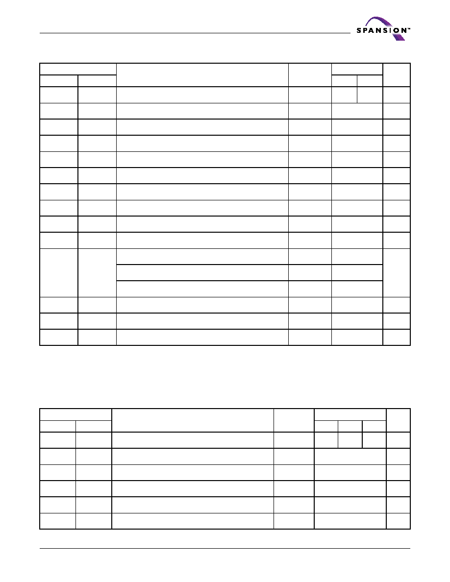
August 4, 2004 S29GLxxxM_00_B1_E
S29GLxxxM MirrorBit
TM
Flash Family
137
D a t a s h e e t
Alternate CE# Controlled Erase and Program Operations-S29GL128M
Notes:
1. Not 100% tested.
2. See the "Erase and Programming Performance" section for more information.
3. For 1≠16 words/1≠32 bytes programmed.
4. If a program suspend command is issued within t
POLL
, the device requires t
POLL
before reading status data, once programming has resumed
(that is, the program resume command has been written). If the suspend command was issued after t
POLL
, status data is available
immediately after programming has resumed. See 24.
Alternate CE# Controlled Erase and Program Operations-S29GL064M
Parameter
Speed Options
Unit
JEDEC
Std.
Description
10
11
t
AVAV
t
WC
Write Cycle Time (Note 1)
Min
100
110
ns
t
AVWL
t
AS
Address Setup Time
Min
0
ns
t
ELAX
t
AH
Address Hold Time
Min
45
ns
t
DVEH
t
DS
Data Setup Time
Min
45
ns
t
EHDX
t
DH
Data Hold Time
Min
0
ns
t
GHEL
t
GHEL
Read Recovery Time Before Write (OE# High to WE# Low)
Min
0
ns
t
WLEL
t
WS
WE# Setup Time
Min
0
ns
t
EHWH
t
WH
WE# Hold Time
Min
0
ns
t
ELEH
t
CP
CE# Pulse Width
Min
35
ns
t
EHEL
t
CPH
CE# Pulse Width High
Min
25
ns
t
WHWH1
t
WHWH1
Write Buffer Program Operation (Notes 2, 3)
Typ
240
µs
Single Word Program Operation (Note 2)
Typ
60
Accelerated Single Word Program Operation (Note 2)
Typ
54
t
WHWH2
t
WHWH2
Sector Erase Operation (Note 2)
Typ
0.5
sec
t
RH
RESET# High Time Before Write
Min
50
ns
t
POLL
Program Valid before Status Polling (Note 4)
Max
4
µs
Parameter
Speed Options
Unit
JEDEC
Std.
Description
90
10
11
t
AVAV
t
WC
Write Cycle Time (Note 1)
Min
90
100
110
ns
t
AVWL
t
AS
Address Setup Time
Min
0
ns
t
ELAX
t
AH
Address Hold Time
Min
45
ns
t
DVEH
t
DS
Data Setup Time
Min
35
ns
t
EHDX
t
DH
Data Hold Time
Min
0
ns
t
GHEL
t
GHEL
Read Recovery Time Before Write (OE# High to WE# Low)
Min
0
ns
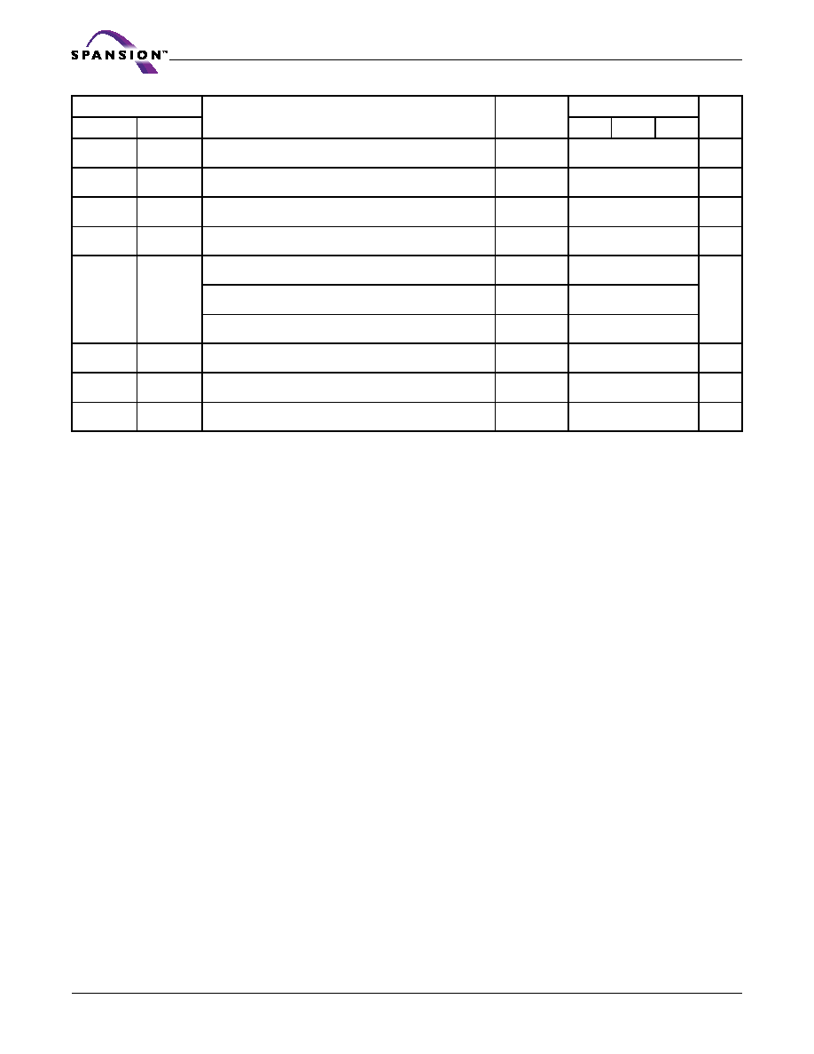
138
S29GLxxxM MirrorBit
TM
Flash Family
S29GLxxxM_00_B1_E August 4, 2004
D a t a s h e e t
Notes:
1. Not 100% tested.
2. See the "Erase and Programming Performance" section for more information.
3. For 1≠16 words/1≠32 bytes programmed.
4. If a program suspend command is issued within t
POLL
, the device requires t
POLL
before reading status data, once programming has resumed
(that is, the program resume command has been written). If the suspend command was issued after t
POLL
, status data is available imme-
diately after programming has resumed. See 24.
t
WLEL
t
WS
WE# Setup Time
Min
0
ns
t
EHWH
t
WH
WE# Hold Time
Min
0
ns
t
ELEH
t
CP
CE# Pulse Width
Min
35
ns
t
EHEL
t
CPH
CE# Pulse Width High
Min
25
ns
t
WHWH1
t
WHWH1
Write Buffer Program Operation (Notes 2, 3)
Typ
240
µs
Single Word Program Operation (Note 2)
Typ
60
Accelerated Single Word Program Operation (Note 2)
Typ
54
t
WHWH2
t
WHWH2
Sector Erase Operation (Note 2)
Typ
0.5
sec
t
RH
RESET# High Time Before Write
Min
50
ns
t
POLL
Program Valid before Status Polling (Note 5)
Max
4
µs
Parameter
Speed Options
Unit
JEDEC
Std.
Description
90
10
11

August 4, 2004 S29GLxxxM_00_B1_E
S29GLxxxM MirrorBit
TM
Flash Family
139
D a t a s h e e t
Alternate CE# Controlled Erase and Program Operations-S29GL032M
Notes:
1. Not 100% tested.
2. See the "Erase and Programming Performance" section for more information.
3. For 1≠16 words/1≠32 bytes programmed.
4. If a program suspend command is issued within t
POLL
, the device requires t
POLL
before reading status data, once programming has resumed
(that is, the program resume command has been written). If the suspend command was issued after t
POLL
, status data is available
immediately after programming has resumed. See 24.
Parameter
Speed Options
Unit
JEDEC
Std.
Description
90
10
11
t
AVAV
t
WC
Write Cycle Time (Note 1)
Min
90
100
110
ns
t
AVWL
t
AS
Address Setup Time
Min
0
ns
t
ELAX
t
AH
Address Hold Time
Min
45
ns
t
DVEH
t
DS
Data Setup Time
Min
35
ns
t
EHDX
t
DH
Data Hold Time
Min
0
ns
t
GHEL
t
GHEL
Read Recovery Time Before Write
(OE# High to WE# Low)
Min
0
ns
t
WLEL
t
WS
WE# Setup Time
Min
0
ns
t
EHWH
t
WH
WE# Hold Time
Min
0
ns
t
ELEH
t
CP
CE# Pulse Width
Min
35
ns
t
EHEL
t
CPH
CE# Pulse Width High
Min
25
ns
t
WHWH1
t
WHWH1
Write Buffer Program Operation (Notes 2, 3)
Typ
240
µs
Single Word Program Operation (Note 2)
Typ
60
Accelerated Single Word Program Operation (Note 2)
Typ
54
t
WHWH2
t
WHWH2
Sector Erase Operation (Note 2)
Typ
0.5
sec
t
RH
RESET# High Time Before Write
Min
50
ns
t
POLL
Program Valid before Status Polling (Note 4)
Max
4
µs

140
S29GLxxxM MirrorBit
TM
Flash Family
S29GLxxxM_00_B1_E August 4, 2004
D a t a s h e e t
Notes:
1. Figure indicates last two bus cycles of a program or erase operation.
2. PA = program address, SA = sector address, PD = program data.
3. DQ7# is the complement of the data written to the device. D
OUT
is the data written to the device.
4. Illustration shows device in word mode.
Figure 24. Alternate CE# Controlled Write (Erase/Program) Operation Timings
t
GHEL
t
WS
OE#
CE#
WE#
RESET#
t
DS
Data
t
AH
Addresses
t
DH
t
CP
DQ7#
D
OUT
t
WC
t
AS
t
CPH
PA
Data# Polling
PBD for program
55 for erase
t
RH
t
WHWH1 or 2
t
POLL
RY/BY#
t
WH
29 for program buffer to flash
30 for sector erase
10 for chip erase
PBA for program
2AA for erase
SA for program buffer to flash
SA for sector erase
555 for chip erase
t
BUSY

August 4, 2004 S29GLxxxM_00_B1_E
S29GLxxxM MirrorBit
TM
Flash Family
141
D a t a s h e e t
Erase and Programming Performance
Notes:
1. Typical program and erase times assume the following conditions: 25∞C, V
CC
= 3.0V, 10,000 cycles; checkerboard data pattern.
2. Under worst case conditions of 90
∞
C; Worst case V
CC
, 100,000 cycles.
3. Effective programming time (typ) is 15 µs (per word), 7.5 µs (per byte).
4. Effective accelerated programming time (typ) is 12.5 µs (per word), 6.3 µs (per byte).
5. Effective write buffer specification is calculated on a per-word/per-byte basis for a 16-word/32-byte write buffer operation.
6. In the pre-programming step of the Embedded Erase algorithm, all bits are programmed to 00h before erasure.
7. System-level overhead is the time required to execute the command sequence(s) for the program command. See Tables 35 and 36 for
further information on command definitions.
Parameter
Typ (Note 1)
Max
(Note 2)
Unit
Comments
Sector Erase Time
0.5
3.5
sec
Excludes
00h
programm
ing prior to
erasure
Note (6)
Chip Erase Time
S29GL032M
32
64
sec
S29GL064M
64
128
S29GL128M
128
256
S29GL256M
256
512
Total Write Buffer Program Time Notes (3), (5)
240
µs
Excludes
system
level
overhead
Note (7)
Total Accelerated Effective Write Buffer Program Time Notes (4),
(5)
200
µs
Chip Program Time
S29GL032M
31.5
sec
S29GL064M
63
S29GL128M
126
S29GL256M
252

142
S29GLxxxM MirrorBit
TM
Flash Family
S29GLxxxM_00_B1_E August 4, 2004
D a t a s h e e t
TSOP Pin and BGA Package Capacitance
For package types TA, TF, BA, BF, FA, FF (refer to Ordering Information Pages):
For package types TB, TC, BB, BC, (refer to Ordering Information Pages):
Notes:
1. Sampled, not 100% tested.
2. Test conditions T
A
= 25∞C, f = 1.0 MHz.
Parameter Symbol
Parameter Description
Test Setup
Typ
Max
Unit
C
IN
Input Capacitance
V
IN
= 0
TSOP
6
7.5
pF
BGA
4.2
5.0
pF
C
OUT
Output Capacitance
V
OUT
= 0
TSOP
8.5
12
pF
BGA
5.4
6.5
pF
C
IN2
Control Pin Capacitance
V
IN
= 0
TSOP
7.5
9
pF
BGA
3.9
4.7
pF
Parameter Symbol
Parameter Description
Test Setup
Typ
Max
Unit
C
IN
Input Capacitance
V
IN
= 0
TSOP
8
10
pF
BGA
8
10
pF
C
OUT
Output Capacitance
V
OUT
= 0
TSOP
8.5
12
pF
BGA
8.5
12
pF
C
IN2
Control Pin Capacitance
V
IN
= 0
TSOP
8
10
pF
BGA
8
10
pF
C
IN3
RESET# and WP#/ACC Pin
Capacitance
V
IN
= 0
TSOP
20
25
pF
BGA
15
20
pF

August 4, 2004 S29GLxxxM_00_B1_E
S29GLxxxM MirrorBit
TM
Flash Family
143
D a t a s h e e t
Physical Dimensions
TS040--40-Pin Standard Thin Small Outline Package
Dwg rev AA; 10/99

144
S29GLxxxM MirrorBit
TM
Flash Family
S29GLxxxM_00_B1_E August 4, 2004
D a t a s h e e t
TSR040--40-Pin Standard/Reverse Thin Small Outline Package (TSOP)
-X-
X = A OR B
e/2
DETAIL B
c
L
0.25MM (0.0098") BSC
0∞
DETAIL A
R
GAGE LINE
PARALLEL TO
SEATING PLANE
b
b1
(c)
7
6
c1
WITH PLATING
BASE METAL
7
C A-B S
M
0.08MM (0.0031")
SECTION B-B
e
0.10 C
A2
PLANE
SEATING
C
A1
SEE DETAIL B
SEE DETAIL B
B
B
B
B
SEE DETAIL A
SEE DETAIL A
2
REVERSE PIN OUT (TOP VIEW)
2
N
+1
N
N
1
4
3
A
-A-
-B-
5
9
E
5
D1
D
6
2
3
4
5
7
8
9
TSR 040
MO-142 (B) EC
40
MIN
0.05
0.95
0.17
0.17
0.10
0.10
18.30
19.80
0.50
0∞
0.08
9.90
0.50 BASIC
MAX
0.15
1.20
0.27
0.16
0.21
5∞
0.20
18.50
10.10
0.70
20.20
0.23
1.05
0.20
1.00
0.22
18.40
20.00
0.60
3∞
10.00
NOM
Symbol
Jedec
Package
b1
A2
A1
A
D
L
e
E
D1
b
c1
c
0
R
N
1
NOTES:
CONTROLLING DIMENSIONS ARE IN MILLIMETERS (MM).
(DIMENSIONING AND TOLERANCING CONFORMS TO ANSI Y14.5M-1982)
NOT APPLICABLE.
PIN 1 IDENTIFIER FOR REVERSE PIN OUT (DIE DOWN), INK OR LASER MARK.
TO BE DETERMINED AT THE SEATING PLANE -C- . THE SEATING PLANE IS DEFINED AS THE PLANE OF
CONTACT THAT IS MADE WHEN THE PACKAGE LEADS ARE ALLOWED TO REST FREELY ON A FLAT
HORIZONTAL SURFACE.
DIMENSIONS D1 AND E DO NOT INCLUDE MOLD PROTRUSION. ALLOWABLE MOLD PROTUSION IS
0.15MM (.0059") PER SIDE.
DIMENSION b DOES NOT INCLUDE DAMBAR PROTUSION. ALLOWABLE DAMBAR PROTUSION SHALL BE
0.08 (0.0031") TOTAL IN EXCESS OF b DIMENSION AT MAX. MATERIAL CONDITION. MINIMUM SPACE
BETWEEN PROTRUSION AND AN ADJACENT LEAD TO BE 0.07 (0.0028").
THESE DIMENSIONS APPLY TO THE FLAT SECTION OF THE LEAD BETWEEN 0.10MM (.0039") AND
0.25MM (0.0098") FROM THE LEAD TIP.
LEAD COPLANARITY SHALL BE WITHIN 0.10MM (0.004") AS MEASURED FROM THE SEATING PLANE.
DIMENSION "e" IS MEASURED AT THE CENTERLINE OF THE LEADS.
3324 \ 16-038.10a

August 4, 2004 S29GLxxxM_00_B1_E
S29GLxxxM MirrorBit
TM
Flash Family
145
D a t a s h e e t
TS048--48-Pin Standard/Reverse Thin Small Outline Package (TSOP)
-X-
X = A OR B
e/2
DETAIL B
c
L
0.25MM (0.0098") BSC
0∞
DETAIL A
R
GAGE LINE
PARALLEL TO
SEATING PLANE
b
b1
(c)
7
6
c1
WITH PLATING
BASE METAL
7
C A-B S
M
0.08MM (0.0031")
SECTION B-B
e
0.10 C
A2
PLANE
SEATING
C
A1
SEE DETAIL B
SEE DETAIL B
B
B
B
B
SEE DETAIL A
SEE DETAIL A
2
STANDARD PIN OUT (TOP VIEW)
2
N
+1
N
N
1
4
2
A
-A-
-B-
5
9
E
5
D1
D
6
2
3
4
5
7
8
9
TS 048
MO-142 (B) EC
48
MIN
0.05
0.95
0.17
0.17
0.10
0.10
18.30
19.80
0.50
0∞
0.08
11.90
0.50 BASIC
MAX
0.15
1.20
0.27
0.16
0.21
5∞
0.20
18.50
12.10
0.70
20.20
0.23
1.05
0.20
1.00
0.22
18.40
20.00
0.60
3∞
12.00
NOM
Symbol
Jedec
Package
b1
A2
A1
A
D
L
e
E
D1
b
c1
c
0
R
N
1
NOTES:
CONTROLLING DIMENSIONS ARE IN MILLIMETERS (MM).
(DIMENSIONING AND TOLERANCING CONFORMS TO ANSI Y14.5M-1982)
PIN 1 IDENTIFIER FOR STANDARD PIN OUT (DIE UP).
NOT APPLICABLE.
TO BE DETERMINED AT THE SEATING PLANE -C- . THE SEATING PLANE IS DEFINED AS THE PLANE OF
CONTACT THAT IS MADE WHEN THE PACKAGE LEADS ARE ALLOWED TO REST FREELY ON A FLAT
HORIZONTAL SURFACE.
DIMENSIONS D1 AND E DO NOT INCLUDE MOLD PROTRUSION. ALLOWABLE MOLD PROTUSION IS
0.15MM (.0059") PER SIDE.
DIMENSION b DOES NOT INCLUDE DAMBAR PROTUSION. ALLOWABLE DAMBAR PROTUSION SHALL BE
0.08 (0.0031") TOTAL IN EXCESS OF b DIMENSION AT MAX. MATERIAL CONDITION. MINIMUM SPACE
BETWEEN PROTRUSION AND AN ADJACENT LEAD TO BE 0.07 (0.0028").
THESE DIMENSIONS APPLY TO THE FLAT SECTION OF THE LEAD BETWEEN 0.10MM (.0039") AND
0.25MM (0.0098") FROM THE LEAD TIP.
LEAD COPLANARITY SHALL BE WITHIN 0.10MM (0.004") AS MEASURED FROM THE SEATING PLANE.
DIMENSION "e" IS MEASURED AT THE CENTERLINE OF THE LEADS.
3325 \ 16-038.10a

146
S29GLxxxM MirrorBit
TM
Flash Family
S29GLxxxM_00_B1_E August 4, 2004
D a t a s h e e t
TSR048--48-Pin Standard/Reverse Thin Small Outline Package (TSOP)
-X-
X = A OR B
e/2
DETAIL B
c
L
0.25MM (0.0098") BSC
0∞
DETAIL A
R
GAGE LINE
PARALLEL TO
SEATING PLANE
b
b1
(c)
7
6
c1
WITH PLATING
BASE METAL
7
C A-B S
M
0.08MM (0.0031")
SECTION B-B
e
0.10 C
A2
PLANE
SEATING
C
A1
SEE DETAIL B
SEE DETAIL B
B
B
B
B
SEE DETAIL A
SEE DETAIL A
2
REVERSE PIN OUT (TOP VIEW)
2
N
+1
N
N
1
4
3
A
-A-
-B-
5
9
E
5
D1
D
6
2
3
4
5
7
8
9
TSR 048
MO-142 (B) EC
48
MIN
0.05
0.95
0.17
0.17
0.10
0.10
18.30
19.80
0.50
0∞
0.08
11.90
0.50 BASIC
MAX
0.15
1.20
0.27
0.16
0.21
5∞
0.20
18.50
12.10
0.70
20.20
0.23
1.05
0.20
1.00
0.22
18.40
20.00
0.60
3∞
12.00
NOM
Symbol
Jedec
Package
b1
A2
A1
A
D
L
e
E
D1
b
c1
c
0
R
N
1
NOTES:
CONTROLLING DIMENSIONS ARE IN MILLIMETERS (MM).
(DIMENSIONING AND TOLERANCING CONFORMS TO ANSI Y14.5M-1982)
NOT APPLICABLE.
PIN 1 IDENTIFIER FOR REVERSE PIN OUT (DIE DOWN), INK OR LASER MARK.
TO BE DETERMINED AT THE SEATING PLANE -C- . THE SEATING PLANE IS DEFINED AS THE PLANE OF
CONTACT THAT IS MADE WHEN THE PACKAGE LEADS ARE ALLOWED TO REST FREELY ON A FLAT
HORIZONTAL SURFACE.
DIMENSIONS D1 AND E DO NOT INCLUDE MOLD PROTRUSION. ALLOWABLE MOLD PROTUSION IS
0.15MM (.0059") PER SIDE.
DIMENSION b DOES NOT INCLUDE DAMBAR PROTUSION. ALLOWABLE DAMBAR PROTUSION SHALL BE
0.08 (0.0031") TOTAL IN EXCESS OF b DIMENSION AT MAX. MATERIAL CONDITION. MINIMUM SPACE
BETWEEN PROTRUSION AND AN ADJACENT LEAD TO BE 0.07 (0.0028").
THESE DIMENSIONS APPLY TO THE FLAT SECTION OF THE LEAD BETWEEN 0.10MM (.0039") AND
0.25MM (0.0098") FROM THE LEAD TIP.
LEAD COPLANARITY SHALL BE WITHIN 0.10MM (0.004") AS MEASURED FROM THE SEATING PLANE.
DIMENSION "e" IS MEASURED AT THE CENTERLINE OF THE LEADS.
3326 \ 16-038.10a
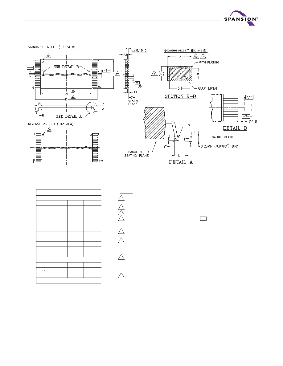
August 4, 2004 S29GLxxxM_00_B1_E
S29GLxxxM MirrorBit
TM
Flash Family
147
D a t a s h e e t
TS056/TSR056--56-Pin Standard/Reverse Thin Small Outline Package (TSOP)
NOTES:
1
CONTROLLING DIMENSIONS ARE IN MILLIMETERS (mm).
(DIMENSIONING AND TOLERANCING CONFORMS TO ANSI Y14.5M-1982.)
2
PIN 1 IDENTIFIER FOR STANDARD PIN OUT (DIE UP).
3
PIN 1 IDENTIFIER FOR REVERSE PIN OUT (DIE DOWN), INK OR LASER MARK.
4
TO BE DETERMINED AT THE SEATING PLANE -C- . THE SEATING PLANE IS
DEFINED AS THE PLANE OF CONTACT THAT IS MADE WHEN THE PACKAGE
LEADS ARE ALLOWED TO REST FREELY ON A FLAT HORIZONTAL SURFACE.
5
DIMENSIONS D1 AND E DO NOT INCLUDE MOLD PROTRUSION. ALLOWABLE
MOLD PROTUSION IS 0.15 mm PER SIDE.
6
DIMENSION b DOES NOT INCLUDE DAMBAR PROTUSION. ALLOWABLE
DAMBAR PROTUSION SHALL BE 0.08 mm TOTAL IN EXCESS OF b
DIMENSION AT MAX MATERIAL CONDITION. MINIMUM SPACE BETWEEN
PROTRUSION AND AN ADJACENT LEAD TO BE 0.07 mm.
7
THESE DIMESIONS APPLY TO THE FLAT SECTION OF THE LEAD BETWEEN
0.10 mm AND 0.25 mm FROM THE LEAD TIP.
8.
LEAD COPLANARITY SHALL BE WITHIN 0.10 mm AS MEASURED FROM THE
SEATING PLANE.
9
DIMENSION "e" IS MEASURED AT THE CENTERLINE OF THE LEADS.
3160\38.10A
MO-142 (B) EC
TS/TSR 56
NOM.
---
---
1.00
1.20
0.15
1.05
MAX.
---
MIN.
0.95
0.20
0.23
0.17
0.22
0.27
0.17
---
0.16
0.10
---
0.21
0.10
20.00
20.20
19.90
14.00
14.10
13.90
0.60
0.70
0.50
3∞
5∞
0∞
---
0.20
0.08
56
18.40
18.50
18.30
0.05
0.50 BASIC
E
R
b1
JEDEC
PACKAGE
SYMBOL
A
A2
A1
D1
D
c1
c
b
e
L
N
O
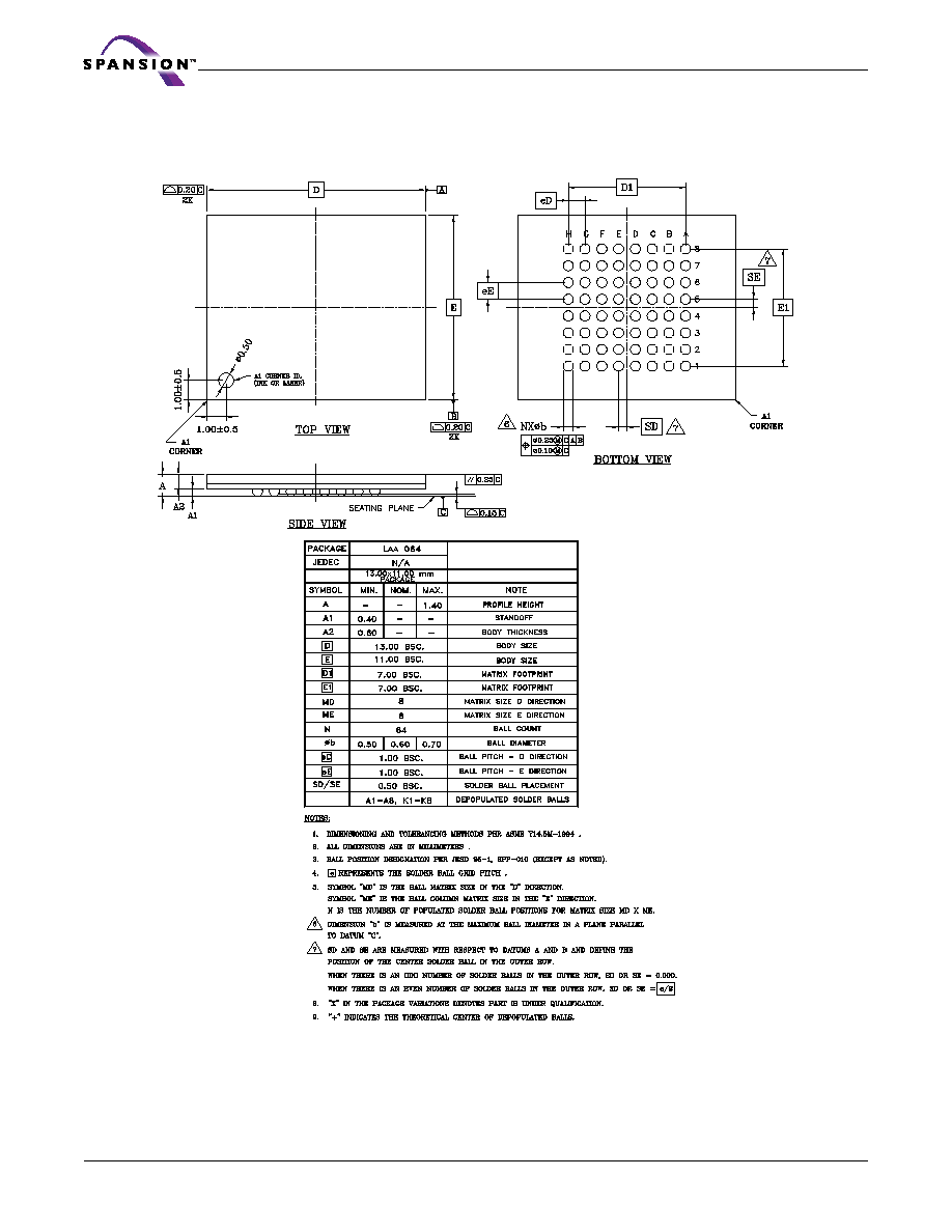
148
S29GLxxxM MirrorBit
TM
Flash Family
S29GLxxxM_00_B1_E August 4, 2004
D a t a s h e e t
LAA064--64-Ball Fortified Ball Grid Array (FBGA)
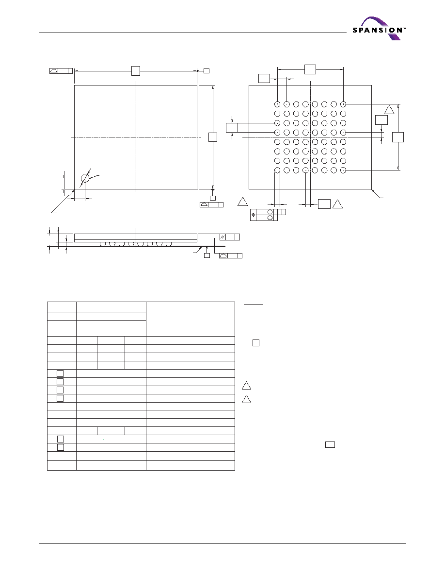
August 4, 2004 S29GLxxxM_00_B1_E
S29GLxxxM MirrorBit
TM
Flash Family
149
D a t a s h e e t
LAC064--64-Pin 18 x 12 mm package
3243 \ 16-038.12d
PACKAGE
LAC 064
JEDEC
N/A
18.00 mm x 12.00 mm
PACKAGE
SYMBOL
MIN
NOM
MAX
NOTE
A
---
---
1.40
PROFILE HEIGHT
A1
0.40
---
---
STANDOFF
A2
0.60
---
---
BODY THICKNESS
D
18.00 BSC.
BODY SIZE
E
12.00 BSC.
BODY SIZE
D1
7.00 BSC.
MATRIX FOOTPRINT
E1
7.00 BSC.
MATRIX FOOTPRINT
MD
8
MATRIX SIZE D DIRECTION
ME
8
MATRIX SIZE E DIRECTION
N
64
BALL COUNT
b
0.50
0.60
0.70
BALL DIAMETER
eD
1.00 BSC.
BALL PITCH - D DIRECTION
eE
1.00 BSC.
BALL PITCH - E DIRECTION
SD / SE
0.50 BSC.
SOLDER BALL PLACEMENT
NONE
DEPOPULATED SOLDER BALLS
NOTES:
1. DIMENSIONING AND TOLERANCING PER ASME Y14.5M-1994.
2. ALL DIMENSIONS ARE IN MILLIMETERS.
3. BALL POSITION DESIGNATION PER JESD 95-1, SPP-010 (EXCEPT
AS NOTED).
4. e REPRESENTS THE SOLDER BALL GRID PITCH.
5. SYMBOL "MD" IS THE BALL ROW MATRIX SIZE IN THE
"D" DIRECTION.
SYMBOL "ME" IS THE BALL COLUMN MATRIX SIZE IN THE
"E" DIRECTION.
N IS THE TOTAL NUMBER OF SOLDER BALLS.
6
DIMENSION "b" IS MEASURED AT THE MAXIMUM BALL
DIAMETER IN A PLANE PARALLEL TO DATUM C.
7
SD AND SE ARE MEASURED WITH RESPECT TO DATUMS
A AND B AND DEFINE THE POSITION OF THE CENTER
SOLDER BALL IN THE OUTER ROW.
WHEN THERE IS AN ODD NUMBER OF SOLDER BALLS IN
THE OUTER ROW PARALLEL TO THE D OR E DIMENSION,
RESPECTIVELY, SD OR SE = 0.000.
WHEN THERE IS AN EVEN NUMBER OF SOLDER BALLS IN
THE OUTER ROW, SD OR SE = e/2
8. NOT USED.
9. "+" INDICATES THE THEORETICAL CENTER OF DEPOPULATED
BALLS.
BOTTOM VIEW
SIDE VIEW
TOP VIEW
2X
2X
C
0.20
C
0.20
6
7
7
A
M
M C
C
0.10
0.25
B
C
0.25
0.15 C
A
B
C
SEATING PLANE
eD
(INK OR LASER)
CORNER
A1
A2
D
E
0.50
A1 CORNER ID.
1.00±0.5
1.00±0.5
A
A1
CORNER
A1
NX
b
SD
SE
eE
E1
D1
1
2
3
4
5
6
7
8
A
C
B
D
F
E
G
H
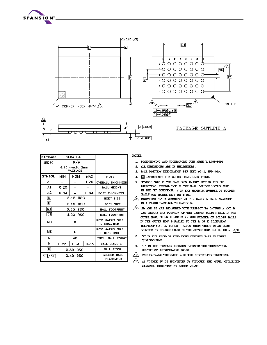
150
S29GLxxxM MirrorBit
TM
Flash Family
S29GLxxxM_00_B1_E August 4, 2004
D a t a s h e e t
FBA048--48-Pin 6.15 x 8.15 mm package
Dwg rev AF; 10/99
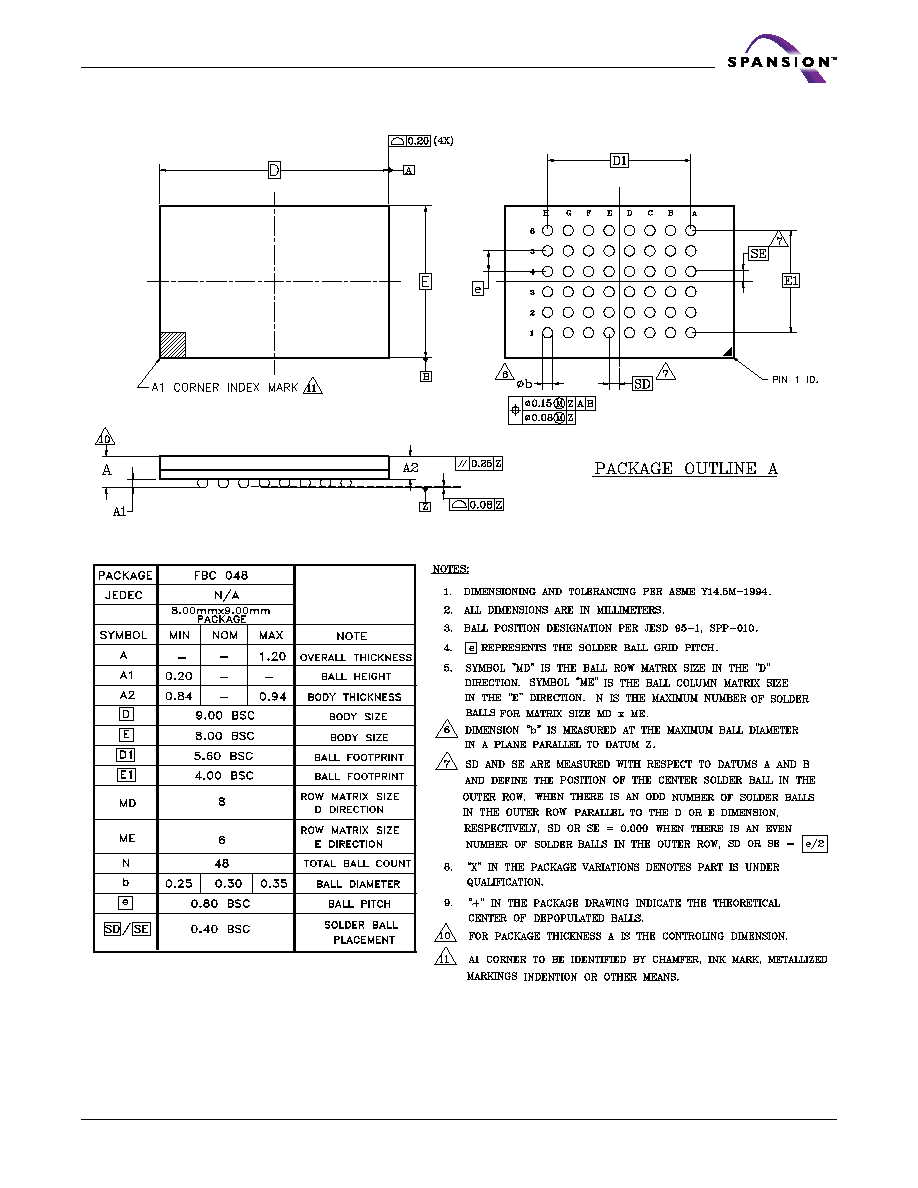
August 4, 2004 S29GLxxxM_00_B1_E
S29GLxxxM MirrorBit
TM
Flash Family
151
D a t a s h e e t
FBC048--48-Pin 8 x 9 mm package
Dwg rev AF; 10/99

152
S29GLxxxM MirrorBit
TM
Flash Family
S29GLxxxM_00_B1_E August 4, 2004
D a t a s h e e t
FBE063--63-Pin 12 x 11 mm package
Dwg rev AF; 10/99
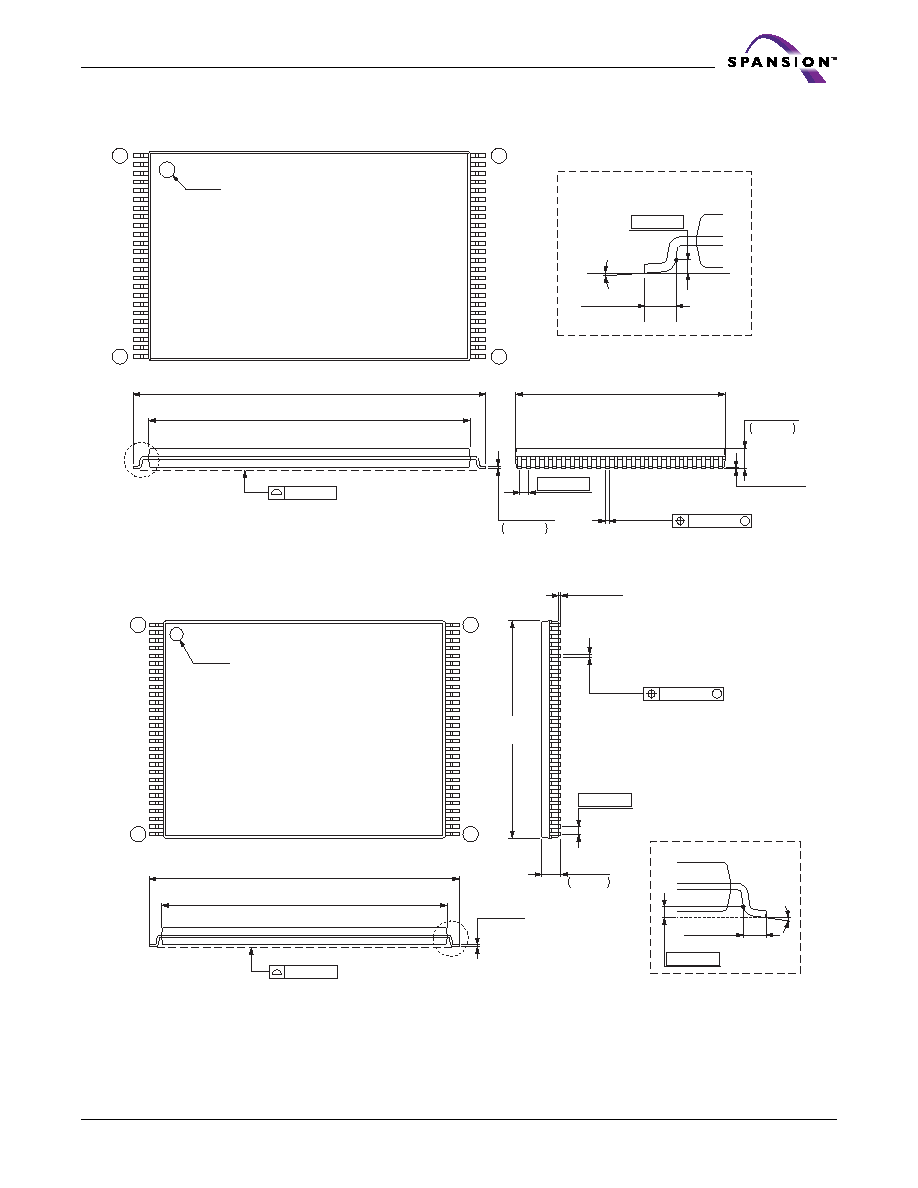
August 4, 2004 S29GLxxxM_00_B1_E
S29GLxxxM MirrorBit
TM
Flash Family
153
D a t a s h e e t
FPT-48P-M19
FPT-56P-M01
≠
.003
+.001
≠
0.08
+0.03
.007
0.17
"A"
(Stand off height)
0.10(.004)
(Mounting
height)
(.472±.008)
12.00
±0.20
LEAD No.
48
25
24
1
(.004
±.002)
0.10(.004)
M
1.10
+0.10
≠
0.05
+.004
≠
.002
.043
0.10
±0.05
(.009
±.002)
0.22
±0.05
(.787
±.008)
20.00
±0.20
(.724
±.008)
18.40
±0.20
INDEX
0~8
∞
0.25(.010)
0.50(.020)
0.60
±0.15
(.024
±.006)
Details of "A" part
*
*
18.40±0.10(.724±.004)
20.00±0.20(.787±.008)
14.00±0.10
M
0.10(.004)
0.10±0.05
(.004±.002)
1
28
56
29
0.08(.003)
(.551±.004)
(Stand off)
LEAD No.
Details of "A" part
0.60±0.15
(.024±.006)
0∞~8∞
.007±.001
0.17±0.03
0.22±0.05
(.009±.002)
(Mounting height)
INDEX
"A"
.043
≠.002
+.004
≠0.05
+0.10
1.10
0.50(.020)
0.25(.010)
*
1
*
2
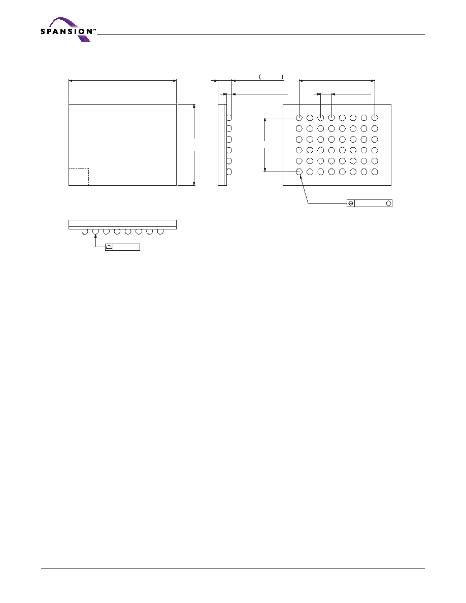
154
S29GLxxxM MirrorBit
TM
Flash Family
S29GLxxxM_00_B1_E August 4, 2004
D a t a s h e e t
BGA-48P-M20
8.00
±0.20(.315±.008)
0.38
±0.10(.015±.004)
(Stand off)
(Mounting height)
6.00
±0.20
(.236
±.008)
0.10(.004)
0.80(.031)TYP
5.60(.220)
4.00(.157)
48-¯0.45
±0.05
(48-¯.018
±.002)
M
¯0.08(.003)
H
G
F
E
D
C
B
A
6
5
4
3
2
1
.043
≠.005
+.003
≠0.13
+0.12
1.08
(INDEX AREA)

August 4, 2004 S29GLxxxM_00_B1_E
S29GLxxxM MirrorBit
TM
Flash Family
155
D a t a s h e e t
Revision Summary
Revision A (January 29, 2004)
Initial Release.
Revision A+1 (February 23, 2004)
Connection Diagrams
Removed 80-ball Fine-pitch BGA pinout.
Ordering Information
Added additional packing type.
Removed frame description from package material set.
Updated valid combinations to reflect the addition of new package type.
Added marking descriptions to all valid combination tables.
Word Program Command Sequence and Unlock Bypass Command Sequence
Added these sections.
Figure 3, "Write Buffer Programming Operation", Figure 4, "Program Operation"
Updated figure.
Table 35, "Command Definitions (x16 Mode, BYTE# = V
IH
),"
Updated table.
Added note 19.
Table 36, "Command Definitions (x8 Mode, BYTE# = V
IL
),"
Updated table.
Added note 17.
Figure 7, "Data# Polling Algorithm"
Updated figure.
Erase and Program Operations and Alternate CE# Controlled Erase and Program Operations
Updated T
WHWHI
description
Added Note 4.
Figure 16
,
Figure 18
,
Figure 20
,
Figure 24
Updated figure.
Physical Dimensions
Removed BGA-63P-M02 and BGA-80P-M01
Added the TS040 package
Revision A+2 (February 25, 2004)
Connection Diagrams
Removed the 40-pin reverse TSOP diagram.
Updated the 48-pin standard TSOP diagram.
Removed the 48-pin reverse TSOP diagram.
Removed the 56-pin reverse TSOP diagram.
Ordering Information
Removed all references to package type R.

156
S29GLxxxM MirrorBit
TM
Flash Family
S29GLxxxM_00_B1_E August 4, 2004
D a t a s h e e t
Table
18
Autoselect Codes, (High Voltage Method)
Updated the R3, R4 column replacing -04 and -03 designators with -R4 and -R3 respectively.
Word Program Command Sequence
Included statements documenting word programming support for backward compatibility with existing Flash
drivers.
Physical Dimensions
Removed the BGA-80P-M02 diagram.
Revision A+3 (February 26, 2004)
Distinctive Characteristics
Corrected typo in the Flexible
Se
ctor Architecture section.
Revision A+4 (March 24, 2004)
CMOS Compatible
Removed V
CC
from Max for V
OL
.
Erase and Program Operations-S29GL256M only
Corrected unit typos.
Erase and Program Operations-S29GL128M only
Corrected the minimum Data Setup Time.
Alternate CE# Controlled Erase and Program Operations-S29GL128M
Corrected the minimum CE# Pulse width.
TSOP Pin and BGA Package Capacitance: Pkg types TB, TC, BB, BC
Added C
IN3.
Connection Diagrams
40-pin standard TSOP: Corrected pin 30 to be V
IO
.
48-pin standard TSOP: Added superscripts to designators for pin 9, 13, 14, 15 and 47. Changed pin 13 to A21.
Added two notes below illustration.
56-pin standard TSOP: Added superscripts to designators for pin 1, 2 and 12. Changed pin 56 to NC. Added three
notes below illustration.
64-ball Fortified BGA: Corrected ball D8 to be V
IO
. Added superscripts to designators for ball D8, F7, and F1.
Added two notes below illustration.
63-ball Fine-pitch BGA: Added superscript to designator for Ball H7. Added one note below illustration. Added con-
nection diagrams for S29GL064M (model R0) and S29GL032M (model R0).
Pin Description
Added V
IO
description.
Logic Symbols
Added V
IO
on all models except R3 and R4.
Figure 3 Write Buffer Programming Operation
Corrected the DQ locations and added callouts to notes one through three.
DC Characteristics
Corrected test conditions for I
CC6
.

August 4, 2004 S29GLxxxM_00_B1_E
S29GLxxxM MirrorBit
TM
Flash Family
157
D a t a s h e e t
Revision A+5 (April 30, 2004)
Ordering Information - S29GL032M
Added R5 and R6 model numbers to the breakout table.
Updated the Valid Combinations for BGA packages table to reflect model numbers R5 and R6.
Ordering Information - S29GL064M
Revised R8 and R9 model numbers on the breakout table.
Updated the Valid Combinations for TSOP packages table.
Ordering Information - S29GL0128M
Added R8 and R9 model numbers to the breakout table.
Revised the Package Material Set options on the breakout table.
Updated the Valid Combinations for TSOP packages table.
Ordering Information - S29GL256M
Revised the Package Material Set options on the breakout table.
Connection Diagrams (56-Pin TSOP)
Added a callout to Note 3 for pin 15.
Device Geometry Definition table
Revised the data and description information for addresses: 28h/50h and
29h/52h.
Primary Vendor Specific Extended Query table
Revised the data and description information for addresses: 45h/8Ah (x16/x8)
Revised the data information for addresses: 4Ch/98h (x16/x8)
Erase and Programming Performance table
Revised notes 1 and 2 below the table.
Revision B0 (May 24, 2004)
Global
Converted to full datasheet status.
Figure 18, "Autoselect Codes, (High Voltage Method)"
Corrected typos in description.
Added values for R5, R6, R7 description for cycle 1-3.
Added R8 and R9 to Model Number.
Revision B1 (August 2, 2004)
"Ordering Information-S29GL032M" on page 21
Added the following temperature range: "C = Commercial (0∞C to +70∞C)'.
Commercial temperature range options added for 90ns speeds.
Global Change
S29GL032M, S29GL064M, S29GL128M, S29GL236M ordering options pages:
Updated note 3 with the following "...TSOPs can be packed in Types 0 and 3; BGAs can be packed in Types 0, 2,
or 3.

158
S29GLxxxM MirrorBit
TM
Flash Family
S29GLxxxM_00_B1_E August 4, 2004
D a t a s h e e t
Colophon
The products described in this document are designed, developed and manufactured as contemplated for general use, including without limita-
tion, ordinary industrial use, general office use, personal use, and household use, but are not designed, developed and manufactured as con-
templated (1) for any use that includes fatal risks or dangers that, unless extremely high safety is secured, could have a serious effect to the
public, and could lead directly to death, personal injury, severe physical damage or other loss (i.e., nuclear reaction control in nuclear facility,
aircraft flight control, air traffic control, mass transport control, medical life support system, missile launch control in weapon system), or (2) for
any use where chance of failure is intolerable (i.e., submersible repeater and artificial satellite). Please note that Spansion will not be liable to
you and/or any third party for any claims or damages arising in connection with above-mentioned uses of the products. Any semiconductor de-
vices have an inherent chance of failure. You must protect against injury, damage or loss from such failures by incorporating safety design mea-
sures into your facility and equipment such as redundancy, fire protection, and prevention of over-current levels and other abnormal operating
conditions. If any products described in this document represent goods or technologies subject to certain restrictions on export under the Foreign
Exchange and Foreign Trade Law of Japan, the US Export Administration Regulations or the applicable laws of any other country, the prior au-
thorization by the respective government entity will be required for export of those products.
Trademarks and Notice
The contents of this document are subject to change without notice. This document may contain information on a Spansion product under development by
Spansion LLC. Spansion LLC reserves the right to change or discontinue work on any product without notice. The information in this document is provided
as is without warranty or guarantee of any kind as to its accuracy, completeness, operability, fitness for particular purpose, merchantability, non-infringement
of third-party rights, or any other warranty, express, implied, or statutory. Spansion LLC assumes no liability for any damages of any kind arising out of the
use of the information in this document.
Copyright © 2004 Spansion LLC. All rights reserved.
Spansion, the Spansion logo, MirrorBit, combinations thereof, and ExpressFlash are trademarks of Spansion LLC. Other company and product names used in
this publication are for identification purposes only and may be trademarks of their respective companies.