
PRELIMINARY
This Data Sheet states Spansion's current technical specifications regarding the Products described herein. This
Data Sheet may be revised by subsequent versions or modifications due to changes in technical specifications.
Publication# S70GL256M00_00Rev: A
Amendment/0
Issue Date: September 8, 2004
S70GL256M00
256 Megabit (8 M x 32-Bit/16 M x 16-Bit) MirrorBit
TM 3.0
Volt-only Uniform Sector Flash Memory with Versatile I/O
TM
Control
Distinctive Characteristics
ARCHITECTURAL ADVANTAGES
Single power supply operation
-- 3 volt read, erase, and program operations
VersatileI/O
TM
control
-- Device generates data output voltages and tolerates
data input voltages on the CE# and DQ inputs/outputs
as determined by the voltage on the V
IO
pin; operates
from 1.65 to 3.6 V
Manufactured on 0.23 µm MirrorBit
TM
process
technology
SecSiTM (Secured Silicon) Sector region
-- 128-doubleword/256-word sector for permanent,
secure identification through an
8-doubleword/16-word random Electronic Serial
Number, accessible through a command sequence
-- May be programmed and locked at the factory or by
the customer
Flexible sector architecture
-- Two hundred fifty-six 32 Kdoubleword (64 Kword)
sectors
Compatibility with JEDEC standards
-- Provides pinout and software compatibility for
single-power supply flash, and superior inadvertent
write protection
100,000 erase cycles typical per sector
20-year data retention typical
PERFORMANCE CHARACTERISTICS
High performance
-- 110 ns access time
-- 30 ns page read times
-- 0.5 s typical sector erase time
-- 15 µs typical write buffer doubleword programming
time: 16-doubleword/32-word write buffer reduces
overall programming time for multiple-word updates
-- 4-doubleword/8-word page read buffer
-- 16-doubleword/32-word write buffer
Low power consumption (typical values at 3.0 V, 5
MHz)
-- 26 mA typical active read current
-- 100 mA typical erase/program current
-- 2 µA typical standby mode current
Package options
-- 80-ball Fortified BGA
SOFTWARE & HARDWARE FEATURES
Software features
-- Program Suspend & Resume: read other sectors
before programming operation is completed
-- Erase Suspend & Resume: read/program other
sectors before an erase operation is completed
-- Data# polling & toggle bits provide status
-- Unlock Bypass Program command reduces overall
programming time
-- CFI (Common Flash Interface) compliant: allows host
system to identify and accommodate multiple flash
devices
Hardware features
-- Sector Group Protection: hardware-level method of
preventing write operations within a sector group
-- Temporary Sector Group Unprotect: V
ID
-level method
of changing code in locked sector groups
-- WP#/ACC input accelerates programming time
(when high voltage is applied) for greater throughput
during system production. Protects first or last sector
group regardless of sector group protection settings
-- Hardware reset input (RESET#) resets device
-- Ready/Busy# output (RY/BY#) detects program or
erase cycle completion

2
S70GL256M00
September 8, 2004
P R E L I M I N A R Y
GENERAL DESCRIPTION
The S70GL256M00 consists of two 128 Mbit, 3.0 volt
single power supply flash memory devices and is or-
ganized as 8,388,608 doublewords or 16,777,216
words. The device has a 32-bit wide data bus that can
also function as an 16-bit wide data bus by using the
WORD# input. The device can be programmed either
in the host system or in standard EPROM program-
mers.
An access time of 110 or 120 ns is available. Note that
each access time has a specific operating voltage
range (V
CC
) as specified in the
Product Selector Guide
and the
Ordering Information
sections. The device is
offered in an 80-ball Fortified BGA package. Each de-
vice has separate chip enable (CE#), write enable
(WE#) and output enable (OE#) controls.
Each device requires only a single 3.0 volt power
supply for both read and write functions. In addition to
a V
CC
input, a high-voltage accelerated program
(WP#/ACC) input provides shorter programming times
through increased current. This feature is intended to
facilitate factory throughput during system production,
but may also be used in the field if desired.
The device is entirely command set compatible with
the JEDEC single-power-supply Flash standard.
Commands are written to the device using standard
microprocessor write timing. Write cycles also inter-
nally latch addresses and data needed for the pro-
gramming and erase operations.
The sector erase architecture allows memory sec-
tors to be erased and reprogrammed without affecting
the data contents of other sectors. The device is fully
erased when shipped from the factory.
Device programming and erasure are initiated through
command sequences. Once a program or erase oper-
ation has begun, the host system need only poll the
DQ7 and DQ15 (Data# Polling) or DQ6 and DQ14
(toggle) status bits or monitor the Ready/Busy#
(RY/BY#) outputs to determine whether the operation
is complete. To facilitate programming, an Unlock By-
pass mode reduces command sequence overhead by
requiring only two write cycles to program data instead
of four.
The VersatileI/OTM (V
IO
) control allows the host sys-
tem to set the voltage levels that the device generates
and tolerates on the CE# control input and DQ I/Os to
the same voltage level that is asserted on the V
IO
pin.
Refer to the Ordering Information section for valid V
IO
options.
Hardware data protection measures include a low
V
CC
detector that automatically inhibits write opera-
tions during power transitions. The hardware sector
group protection feature disables both program and
erase operations in any combination of sector groups
of memory. This can be achieved in-system or via pro-
gramming equipment.
The Erase Suspend/Erase Resume feature allows
the host system to pause an erase operation in a given
sector to read or program any other sector and then
complete the erase operation. The Program Sus-
pend/Program Resume feature enables the host sys-
tem to pause a program operation in a given sector to
read any other sector and then complete the program
operation.
The hardware RESET# pin terminates any operation
in progress and resets the device, after which it is then
ready for a new operation. The RESET# pin may be
tied to the system reset circuitry. A system reset would
thus also reset the device, enabling the host system to
read boot-up firmware from the Flash memory device.
T h e d evice re d uce s p ow er co ns ump ti on i n th e
standby mode when it detects specific voltage levels
on CE# and RESET#, or when addresses have been
stable for a specified period of time.
The SecSi
TM (Secured Silicon) Sector provides a
128-doubleword/256-word area for code or data that
can be permanently protected. Once this sector is pro-
tected, no further changes within the sector can occur.
The Write Protect (WP#/ACC) feature protects the
first or last sector by asserting a logic low on the WP#
pin.
Spansion MirrorBit
TM
flash technology combines years
of Flash memory manufacturing experience to pro-
duce the highest levels of quality, reliability and cost
effectiveness. The device electrically erases all bits
within a sector simultaneously via hot-hole assisted
erase. The data is programmed using hot electron in-
jection.
RELATED DOCUMENTS
For a comprehensive information on MirrorBit prod-
ucts, including migration information, data sheets, ap-
plication notes, and software drivers, please see
www.amd.com
Flash Memory
Product Informa-
tion
MirrorBit
Flash Information
Technical Docu-
mentation.
The following is a partial list of documents
closely related to this product:
MirrorBitTM Flash Memory Write Buffer Programming
and Page Buffer Read
Implementing a Common Layout for Spansion Mirror-
Bit and Intel StrataFlash Memory Devices
Migrating from Single-byte to Three-byte Device IDs

September 8, 2004
S70GL256M00
3
P R E L I M I N A R Y
TABLE OF CONTENTS
Product Selector Guide . . . . . . . . . . . . . . . . . . . . . 4
MCP Block Diagram . . . . . . . . . . . . . . . . . . . . . . . . 4
Flash Memory Block diagram . . . . . . . . . . . . . . . . 5
Special Package Handling Instructions .................................... 6
Pin Configuration . . . . . . . . . . . . . . . . . . . . . . . . . . 7
Logic Symbols . . . . . . . . . . . . . . . . . . . . . . . . . . . . 7
x16 Mode .................................................................................. 7
x32 Mode .................................................................................. 7
Ordering Information . . . . . . . . . . . . . . . . . . . . . . . 8
Device Bus Operations . . . . . . . . . . . . . . . . . . . . . 9
Table 1. Device Bus Operations ....................................................... 9
Word/Byte Configuration .......................................................... 9
VersatileIO
TM
(V
IO
) Control ........................................................ 9
Requirements for Reading Array Data ................................... 10
Page Mode Read ............................................................................10
Writing Commands/Command Sequences ............................ 10
Write Buffer .....................................................................................10
Accelerated Program Operation ......................................................10
Autoselect Functions .......................................................................10
Standby Mode ........................................................................ 10
Automatic Sleep Mode ........................................................... 11
RESET#: Hardware Reset Pin ............................................... 11
Output Disable Mode .............................................................. 11
Table 2. Sector Address Table........................................................ 12
Autoselect Mode ..................................................................... 18
Table 3. Autoselect Codes, (High Voltage Method) ....................... 18
Sector Group Protection and Unprotection ............................. 19
Table 4. Sector Group Protection/Unprotection Address Table ..... 19
Write Protect (WP#) ................................................................ 20
Temporary Sector Group Unprotect ....................................... 20
Figure 1. Temporary Sector Group Unprotect Operation ................20
Figure 2. In-System Sector Group Protect/Unprotect Algorithms ...21
SecSi (Secured Silicon) Sector Flash Memory Region .......... 22
Table 5. SecSi Sector Contents ...................................................... 22
Figure 3. SecSi Sector Protect Verify ..............................................23
Hardware Data Protection ...................................................... 23
Low VCC Write Inhibit .....................................................................23
Write Pulse "Glitch" Protection ........................................................23
Logical Inhibit ..................................................................................23
Power-Up Write Inhibit ....................................................................23
Common Flash Memory Interface (CFI) . . . . . . . 23
Reading Array Data ................................................................ 27
Reset Command ..................................................................... 27
Autoselect Command Sequence ............................................ 27
Enter SecSi Sector/Exit SecSi Sector Command Sequence .. 28
Doubleword/Word Program Command Sequence ................. 28
Unlock Bypass Command Sequence ..............................................28
Write Buffer Programming ...............................................................28
Accelerated Program ......................................................................29
Figure 4. Write Buffer Programming Operation ...............................30
Figure 5. Program Operation ..........................................................31
Program Suspend/Program Resume Command Sequence ... 31
Figure 6. Program Suspend/Program Resume ...............................32
Chip Erase Command Sequence ........................................... 32
Sector Erase Command Sequence ........................................ 32
Figure 7. Erase Operation .............................................................. 33
Erase Suspend/Erase Resume Commands ........................... 33
Command Definitions ............................................................. 34
Write Operation Status . . . . . . . . . . . . . . . . . . . . . 36
DQ7 and DQ5: Data# Polling .................................................. 36
Figure 8. Data# Polling Algorithm .................................................. 36
RY/BY#: Ready/Busy# ............................................................ 37
DQ6 and DQ14: Toggle Bits I ................................................. 37
Figure 9. Toggle Bit Algorithm ........................................................ 38
DQ2 and DQ10: Toggle Bits II ................................................ 38
Reading Toggle Bits DQ6 and DQ14/DQ2 and DQ10 ............ 38
DQ5 and DQ13: Exceeded Timing Limits ............................... 39
DQ3 and DQ11: Sector Erase Timer ...................................... 39
DQ1: Write-to-Buffer Abort ..................................................... 40
Table 12. Write Operation Status................................................... 40
Figure 10. Maximum Negative Overshoot Waveform .................... 41
Figure 11. Maximum Positive Overshoot Waveform ...................... 41
Operating Ranges . . . . . . . . . . . . . . . . . . . . . . . . . 41
DC Characteristics . . . . . . . . . . . . . . . . . . . . . . . . 42
Figure 12. Test Setup ..................................................................... 43
Table 13. Test Specifications ......................................................... 43
Key to Switching Waveforms. . . . . . . . . . . . . . . . 43
Figure 13. Input Waveforms and
Measurement Levels ...................................................................... 43
AC Characteristics . . . . . . . . . . . . . . . . . . . . . . . . 44
Read-Only Operations ............................................................ 44
Figure 14. Read Operation Timings ............................................... 44
Figure 15. Page Read Timings ...................................................... 45
Hardware Reset (RESET#) .................................................... 46
Figure 16. Reset Timings ............................................................... 46
Erase and Program Operations .............................................. 47
Figure 17. Program Operation Timings .......................................... 48
Figure 18. Accelerated Program Timing Diagram .......................... 48
Figure 19. Chip/Sector Erase Operation Timings .......................... 49
Figure 20. Data# Polling Timings (During Embedded Algorithms) . 50
Figure 21. Toggle Bit Timings (During Embedded Algorithms) ...... 51
Figure 22. DQ2 vs. DQ6 ................................................................. 51
Temporary Sector Unprotect .................................................. 52
Figure 23. Temporary Sector Group Unprotect Timing Diagram ... 52
Figure 24. Sector Group Protect and Unprotect Timing Diagram .. 53
Alternate CE# Controlled Erase and Program Operations ..... 54
Figure 25. Alternate CE# Controlled Write (Erase/Program)
Operation Timings ...............................................................................55
Latchup Characteristics . . . . . . . . . . . . . . . . . . . . 55
Erase And Programming Performance. . . . . . . . 56
TSOP Pin and BGA Package Capacitance . . . . . 56
Data Retention. . . . . . . . . . . . . . . . . . . . . . . . . . . . 56
LSB080≠80-Ball Fortified Ball Grid Array (Fortified BGA)
13 x 11 mm Package .............................................................. 57
Revision Summary . . . . . . . . . . . . . . . . . . . . . . . . 58
4
S70GL256M00
September 8, 2004
P R E L I M I N A R Y
PRODUCT SELECTOR GUIDE
MCP BLOCK DIAGRAM
Note: In x16 Mode, DQ31 and DQ23 must be connected together on the board.
Part Number
S70GL256M00
Speed Option
V
CC
= 3.0
≠
3.6 V
110R
(V
IO
= 2.7
≠
3.6 V)
120R
(V
IO
= 1.65
≠
3.6 V)
Max. Access Time (ns)
110
120
Max. CE# Access Time (ns)
110
120
Max. Page access time (t
PACC
)
30
30
Max. OE# Access Time (ns)
30
30
OE#
WE#
CE#
128 Mbit
Flash Memory
#2
128 Mbit
Flash Memory
#1
DQ23/A-1 to DQ16; DQ7-DQ0
DQ31/A-1 to DQ24; DQ15 TO DQ8
DQ31 to DQ0
A23 to A0
RY/BY#
RESET#
X16
X16
X32
WORD#
WP#/ACC
September 8, 2004
S70GL256M00
5
P R E L I M I N A R Y
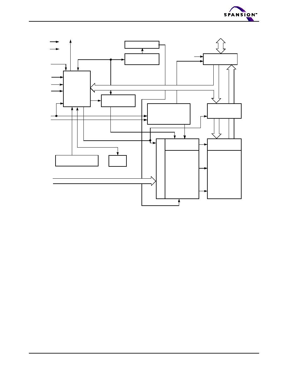
FLASH MEMORY BLOCK DIAGRAM
Note:
1. In x16 Mode, DQ31 and DQ23 must be connected together on the board.
Input/Output
Buffers
X-Decoder
Y-Decoder
Chip Enable
Output Enable
Logic
Erase Voltage
Generator
PGM Voltage
Generator
Timer
V
CC
Detector
State
Control
Command
Register
V
CC
V
SS
WE#
WP#/ACC
WORD#
CE#
OE#
STB
STB
DQ31
≠
DQ0 (A-1)
Sector Switches
RY/BY#
RESET#
Data
Latch
Y-Gating
Cell Matrix
Ad
dre
ss L
a
tc
h
A22≠A0
V
IO
6
S70GL256M00
September 8, 2004
P R E L I M I N A R Y
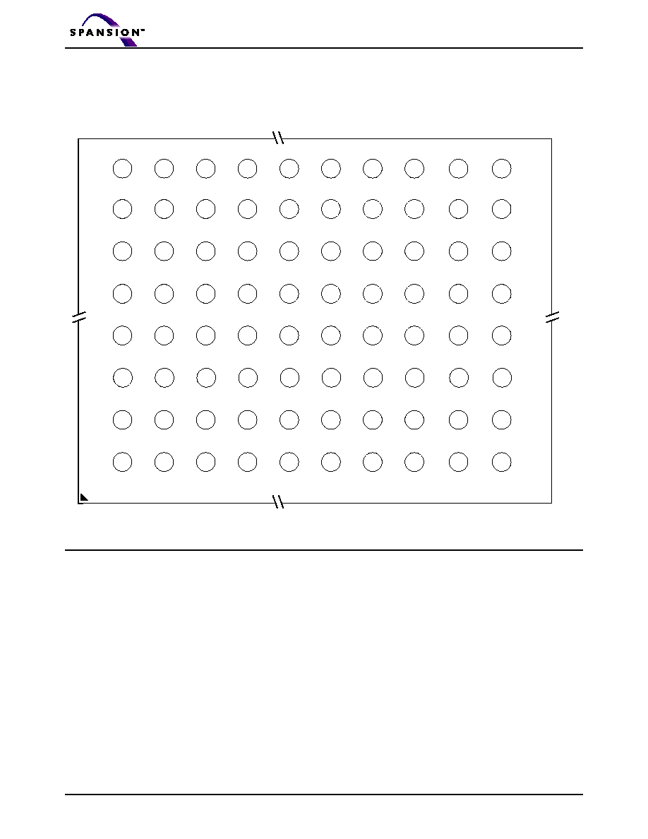
CONNECTION DIAGRAMS
Note: The FBGA package pinout configuration shown is preliminary. The ball count and package physical dimensions have not
yet been determined. Contact Spansion for further information.
Special Package Handling Instructions
Special handling is required for Flash Memory products
in molded packages (BGA). The package and/or data
integrity may be compromised if the package body is
exposed to temperatures above 150∞C for prolonged
periods of time.
80-ball Fortified BGA
Top View, Balls Facing Down
A2
C2
D2
E2
F2
G2
H2
A3
C3
D3
E3
F3
G3
H3
A4
C4
D4
E4
F4
G4
H4
A5
C5
D5
E5
F5
G5
H5
A6
C6
D6
E6
F6
G6
H6
A7
C7
D7
E7
F7
G7
H7
WORD#
DQ15
A16
A15
A14
A12
A13
DQ23/A-1
DQ14
DQ13
DQ7
A11
A10
A8
A9
DQ30
DQ12
V
CC
DQ5
A19
A21
RESET#
WE#
V
SS
DQ10
DQ11
DQ2
A20
A18
WP#/ACC
RY/BY#
V
CC
DQ8
DQ9
DQ0
A5
A6
A17
A7
DQ31/A-1
CE#
OE#
A0
A1
A2
A4
A3
DQ18
A1
C1
D1
E1
F1
G1
H1
V
IO
RFU
RFU
RFU
RFU
V
CC
DQ16
RFU
A8
C8
B2
B3
B4
B5
B6
B7
B1
B8
D8
E8
F8
G8
H8
RFU
RFU
J2
J3
J4
J5
J6
J7
V
SS
DQ6
DQ4
DQ3
DQ1
V
SS
J1
DQ24
J8
DQ29
K2
K3
K4
K5
K6
K7
DQ20
DQ27
DQ26
DQ19
DQ17
V
CC
K1
DQ25
K8
DQ22
V
SS
V
IO
RFU
A22
DQ28
DQ21
September 8, 2004
S70GL256M00
7
P R E L I M I N A R Y
PIN CONFIGURATION
A
≠1
= Least significant address bit for the 16-bit
data bus, and selects between the high
and low word. A ≠1 is not used for the
32-bit mode (WORD# = V
IH
).
A22≠A0
= 23-bit address bus for 256 Mb device.
DQ31≠DQ0
= 32-bit data inputs/outputs/float
WORD#
= Selects 16-bit or 32-bit mode. When
WORD# = V
IH
, data is output on
DQ31≠DQ0. When WORD# = V
IL
, data is
output on DQ15≠DQ0.
CE#
= Chip Enable Input.
OE#
= Output Enable Input.
WE#
= Write enable.
V
SS
= Device ground
RY/BY#
= Ready/Busy output and open drain. When
RY/BY# = V
OH
, the device is ready to ac-
cept read operations and commands.
When RY/BY# = V
OL
, the device is either
executing an embedded algorithm or the
device is executing a hardware reset oper-
ation.
WP#/ACC
= Write Protect input/Acceleration input.
V
CC
= Power Supply (2.7 V to 3.6 V)
RESET#
= Hardware reset input
NC
= Pin not connected internally
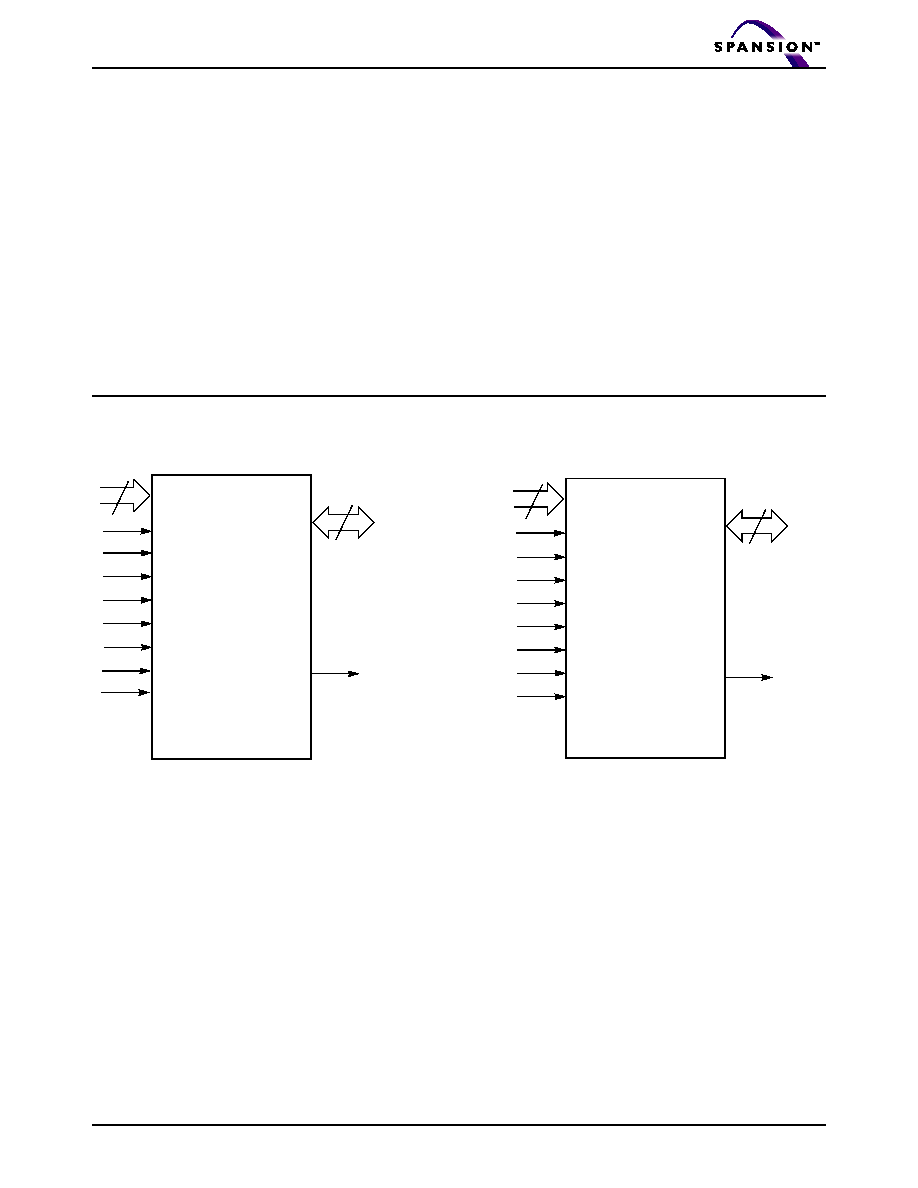
LOGIC SYMBOLS
x16 Mode
x32 Mode
Note:In x16 mode, DQ31 and DQ23 must be connected to each other on the board.
24
16
DQ15≠DQ0
A22 to A-1
RY/BY#
CE#
OE#
WE#
WP#/ACC
RESET#
WP#
WORD#
V
IO
23
32
DQ31≠DQ0
A22≠A0
RY/BY#
CE#
OE#
WE#
WP#/ACC
RESET#
WP#
WORD#
V
IO
8
S70GL256M00
September 8, 2004
P R E L I M I N A R Y
ORDERING INFORMATION
Standard Products
Spansion standard products are available in several packages and operating ranges. The order number (Valid Combination) is
formed by a combination of the following:
Valid Combinations
Valid Combinations list configurations planned to be supported in vol-
ume for this device. Consult the local Spansion sales office to confirm
availability of specific valid combinations and to check on newly re-
leased combinations.
S70GL256M00
F
A
I
RA
0
PACKING TYPE
0
= Tray (Standard, see Note 1)
MODEL NUMBER
RA
= V
CC
= Regulate (3.0-3.6V), 110ns; highest address sector protected)
RB
= V
CC
= Regulate (3.0-3.6V), 110ns; lowest address sector protected)
RC
= V
CC
= Regulate (3.0-3.6V), 120ns; highest address sector protected)
RD
= V
CC
= Regulate (3.0-3.6V), 120ns; lowest address sector protected)
TEMPERATURE RANGE
I
=
Industrial (-40∞C to +85∞C)
PACKAGING MATERIAL SET
A
=
Standard
F
=
Pb-free
PACKAGE TYPE
F
=
Fortified Ball Grid Array, 1.0 mm pitch package
DEVICE NUMBER/DESCRIPTION
S70GL256M00
3.0 Volt-only, 256 Megabit (8/16M x 32/16-Bit), Page-Mode Flash Memory
S29GL512N Valid Combinations
Order Number
Package &
Temperature
Model
Number
Pack Type
Package
Description
S70GL256M00
FAI, FFI
RA, RB
RC, RD
0 (Note 1)
LSB080
(Fortified BGA)
September 8, 2004
S70GL256M00
9
P R E L I M I N A R Y
DEVICE BUS OPERATIONS
This section describes the requirements and use of
the device bus operations, which are initiated through
the internal command register. The command register
itself does not occupy any addressable memory loca-
tion. The register is a latch used to store the com-
mands, along with the address and data information
needed to execute the command. The contents of the
register serve as inputs to the internal state machine.
The state machine outputs dictate the function of the
device. Table 1 lists the device bus operations, the in-
puts and control levels they require, and the resulting
output. The following subsections describe each of
these operations in further detail.
Table 1.
Device Bus Operations
Legend: L = Logic Low = V
IL
, H = Logic High = V
IH
, V
ID
= 11.5≠12.5 V, V
HH
= 11.5≠12.5V, X = Don't Care, SA = Sector Address,
A
IN
= Address In, D
IN
= Data In, D
OUT
= Data Out
Notes:
1. Addresses are A22:A0 in doubleword mode; A22:A-1 in word mode. Sector addresses are A22:A15 in both modes.
2. The sector group protect and sector group unprotect functions may also be implemented via programming equipment. See the
"Sector Group Protection and Unprotection" section.
3. If WP# = V
IL
, the first or last sector group remains protected. If WP# = V
IH
, the first or last sector will be protected or unprotected as
determined by the method described in "Write Protect (WP#)". All sectors are unprotected when shipped from the factory (The
SecSi Sector may be factory protected depending on version ordered.)
4. D
IN
or D
OUT
as required by command sequence, data polling, or sector protect algorithm (see Figure 2).
Word/Byte Configuration
The WORD# pin controls whether the device data I/O
pins operate in the word or doubleword configuration.
If the WORD# pin is set at V
IH
, the device is in double-
word configuration, DQ31≠DQ0 are active and con-
trolled by CE# and OE#.
If the WORD# pin is set at V
IL
, the device is in word
configuration, and only data I/O pins DQ15≠DQ0 are
active and controlled by CE# and OE#. The data I/O
pins DQ31≠DQ16 are tri-stated, and the DQ23 and
DQ31 pins are used as inputs for the LSB (A-1) ad-
dress function.
VersatileIO
TM
(V
IO
) Control
The VersatileIO
TM
(V
IO
) control allows the host system
to set the voltage levels that the device generates and
tolerates on CE# and DQ I/Os to the same voltage
level that is asserted on V
IO
. See Ordering Information
for V
IO
options on this device.
Operation
CE#
OE#
WE#
RESET#
WP#
ACC
Addresses
(Note 1)
DQ15≠
DQ0
DQ31≠DQ16
WORD#
= V
IH
WORD#
= V
IL
Read
L
L
H
H
X
X
A
IN
D
OUT
D
OUT
DQ31≠DQ16
= High-Z,
DQ31 &
DQ23= A-1
Write (Program/Erase)
L
H
L
H
(Note 3)
X
A
IN
(Note 4) (Note 4)
Accelerated Program
L
H
L
H
(Note 3)
V
HH
A
IN
(Note 4) (Note 4)
Standby
V
CC
±
0.3 V
X
X
V
CC
±
0.3 V
X
H
X
High-Z
High-Z
High-Z
Output Disable
L
H
H
H
X
X
X
High-Z
High-Z
High-Z
Reset
X
X
X
L
X
X
X
High-Z
High-Z
High-Z
Sector Group Protect
(Note 2)
L
H
L
V
ID
H
X
SA, A6 =L,
A3=L, A2=L,
A1=H, A0=L
(Note 4)
X
X
Sector Group Unprotect
(Note 2)
L
H
L
V
ID
H
X
SA, A6=H,
A3=L, A2=L,
A1=H, A0=L
(Note 4)
X
X
Temporary Sector Group
Unprotect
X
X
X
V
ID
H
X
A
IN
(Note 4) (Note 4)
High-Z

10
S70GL256M00
September 8, 2004
P R E L I M I N A R Y
Requirements for Reading Array Data
To read array data from the outputs, the system must
drive the CE# and OE# pins to V
IL
. CE# is the power
control and selects the device. OE# is the output con-
trol and gates array data to the output pins. WE#
should remain at V
IH
.
The internal state machine is set for reading array data
upon device power-up, or after a hardware reset. This
ensures that no spurious alteration of the memory
content occurs during the power transition. No com-
mand is necessary in this mode to obtain array data.
Standard microprocessor read cycles that assert valid
addresses on the device address inputs produce valid
data on the device data outputs. The device remains
enabled for read access until the command register
contents are altered.
See "Reading Array Data" for more information. Refer
to the AC Read-Only Operations table for timing speci-
fications and to Figure 14 for the timing diagram. Refer
to the DC Characteristics table for the active current
specification on reading array data.
Page Mode Read
The device is capable of fast page mode read and is
compatible with the page mode Mask ROM read oper-
ation. This mode provides faster read access speed
for random locations within a page. The page size of
the device is 4 doublewords/8 words. The appropriate
p a g e i s s e l e c t e d b y t h e h i g h e r a d d r e s s b i t s
A(max)≠A2. Address bits A1≠A0 in doubleword mode
(A1≠A-1 in word mode) determine the specific word
within a page. This is an asynchronous operation; the
microprocessor supplies the specific word location.
The random or initial page access is equal to t
ACC
or
t
CE
and subsequent page read accesses (as long as
the locations specified by the microprocessor falls
within that page) is equivalent to t
PACC
. When CE# is
deasserted and reasserted for a subsequent access,
the access time is t
ACC
or t
CE
. Fast page mode ac-
cesses are obtained by keeping the "read-page ad-
dresses" constant and changing the "intra-read page"
addresses.
Writing Commands/Command Sequences
To write a command or command sequence (which in-
cludes programming data to the device and erasing
sectors of memory), the system must drive WE# and
CE# to V
IL
, and OE# to V
IH
.
The device features an Unlock Bypass mode to facili-
tate faster programming. Once the device enters the
Unlock Bypass mode, only two write cycles are re-
quired to program a word or byte, instead of four. The
"Doubleword/Word Program Command Sequence"
section has details on programming data to the device
using both standard and Unlock Bypass command se-
quences.
An erase operation can erase one sector, multiple sec-
tors, or the entire device. Table 2 indicates the address
space that each sector occupies.
Refer to the DC Characteristics table for the active
current specification for the write mode. The AC Char-
acteristics section contains timing specification tables
and timing diagrams for write operations.
Write Buffer
Write Buffer Programming allows the system write to a
maximum of 16 doublewords/32 words in one pro-
gramming operation. This results in faster effective
programming time than the standard programming al-
gorithms. See "Write Buffer" for more information.
Accelerated Program Operation
The device offers accelerated program operations
through the ACC function. This is one of two functions
provided by the WP#/ACC pin. This function is prima-
rily intended to allow faster manufacturing throughput
at the factory.
If the system asserts V
HH
on this pin, the device auto-
matically enters the aforementioned Unlock Bypass
mode, temporarily unprotects any protected sector
groups, and uses the higher voltage on the pin to re-
duce the time required for program operations. The
system would use a two-cycle program command se-
quence as required by the Unlock Bypass mode. Re-
moving V
HH
from the WP#/ACC pin returns the device
to normal operation.
Note that the WP#/ACC pin must
not be at V
HH
for operations other than accelerated
programming, or device damage may result. WP# has
an internal pullup; when unconnected, WP# is at V
IH
.
Autoselect Functions
If the system writes the autoselect command se-
quence, the device enters the autoselect mode. The
system can then read autoselect codes from the inter-
nal register (which is separate from the memory array)
on DQ7≠DQ0. Standard read cycle timings apply in
this mode. Refer to the Autoselect Mode and Autose-
lect Command Sequence sections for more informa-
tion.
Standby Mode
When the system is not reading or writing to the de-
vice, it can place the device in the standby mode. In
this mode, current consumption is greatly reduced,
and the outputs are placed in the high impedance
state, independent of the OE# input.
The device enters the CMOS standby mode when the
CE# and RESET# pins are both held at V
CC
± 0.3 V.
(Note that this is a more restricted voltage range than

September 8, 2004
S70GL256M00
11
P R E L I M I N A R Y
V
IH
.) If CE# and RESET# are held at V
IH
, but not within
V
CC
± 0.3 V, the device will be in the standby mode,
but the standby current will be greater. The device re-
quires standard access time (t
CE
) for read access
when the device is in either of these standby modes,
before it is ready to read data.
If the device is deselected during erasure or program-
ming , the device draws active current until th e
operation is completed.
Refer to the DC Characteristics table for the standby
current specification.
Automatic Sleep Mode
The automatic sleep mode minimizes Flash device en-
ergy consumption. The device automatically enables
this mode when addresses remain stable for t
ACC
+
30 ns. The automatic sleep mode is independent of
the CE#, WE#, and OE# control signals. Standard ad-
dress access timings provide new data when ad-
dresses are changed. While in sleep mode, output
data is latched and always available to the system.
Refer to the DC Characteristics table for the automatic
sleep mode current specification.
RESET#: Hardware Reset Pin
The RESET# pin provides a hardware method of re-
setting the device to reading array data. When the RE-
SET# pin is driven low for at least a period of t
RP
, the
device immediately terminates any operation in
progress, tristates all output pins, and ignores all
read/write commands for the duration of the RESET#
pulse. The device also resets the internal state ma-
chine to reading array data. The operation that was in-
terrupted should be reinitiated once the device is
ready to accept another command sequence, to en-
sure data integrity.
Current is reduced for the duration of the RESET#
pulse. When RESET# is held at V
SS
±0.3 V, the device
draws CMOS standby current (I
CC4
). If RESET# is held
at V
IL
but not within V
SS
±0.3 V, the standby current will
be greater.
The RESET# pin may be tied to the system reset cir-
cuitry. A system reset would thus also reset the Flash
memory, enabling the system to read the boot-up firm-
ware from the Flash memory.
Refer to the AC Characteristics tables for RESET# pa-
rameters and to Figure 16 for the timing diagram.
Output Disable Mode
When the OE# input is at V
IH
, output from the device is
disabled. The output pins are placed in the high
impedance state.
12
S70GL256M00
September 8, 2004
P R E L I M I N A R Y
Table 2.
Sector Address Table
Sector
A22≠A15
Sector Size
(Kwords/Kdoublewords)
16-bit
Address Range
(in hexadecimal)
32-bit
Address Range
(in hexadecimal)
SA0
0
0
0
0
0
0
0
0
64/32
000000≠00FFFF
000000≠007FFF
SA1
0
0
0
0
0
0
0
1
64/32
010000≠01FFFF
008000≠00FFFF
SA2
0
0
0
0
0
0
1
0
64/32
020000≠02FFFF
010000≠017FFF
SA3
0
0
0
0
0
0
1
1
64/32
030000≠03FFFF
018000≠01FFFF
SA4
0
0
0
0
0
1
0
0
64/32
040000≠04FFFF
020000≠027FFF
SA5
0
0
0
0
0
1
0
1
64/32
050000≠05FFFF
028000≠02FFFF
SA6
0
0
0
0
0
1
1
0
64/32
060000≠06FFFF
030000≠037FFF
SA7
0
0
0
0
0
1
1
1
64/32
070000≠07FFFF
038000≠03FFFF
SA8
0
0
0
0
1
0
0
0
64/32
080000≠08FFFF
040000≠047FFF
SA9
0
0
0
0
1
0
0
1
64/32
090000≠09FFFF
048000≠04FFFF
SA10
0
0
0
0
1
0
1
0
64/32
0A0000≠0AFFFF
050000≠057FFF
SA11
0
0
0
0
1
0
1
1
64/32
0B0000≠0BFFFF
058000≠05FFFF
SA12
0
0
0
0
1
1
0
0
64/32
0C0000≠0CFFFF
060000≠067FFF
SA13
0
0
0
0
1
1
0
1
64/32
0D0000≠0DFFFF
068000≠06FFFF
SA14
0
0
0
0
1
1
1
0
64/32
0E0000≠0EFFFF
070000≠077FFF
SA15
0
0
0
0
1
1
1
1
64/32
0F0000≠0FFFFF
078000≠07FFFF
SA16
0
0
0
1
0
0
0
0
64/32
100000≠10FFFF
080000≠087FFF
SA17
0
0
0
1
0
0
0
1
64/32
110000≠11FFFF
088000≠08FFFF
SA18
0
0
0
1
0
0
1
0
64/32
120000≠12FFFF
090000≠097FFF
SA19
0
0
0
1
0
0
1
1
64/32
130000≠13FFFF
098000≠09FFFF
SA20
0
0
0
1
0
1
0
0
64/32
140000≠14FFFF
0A0000≠0A7FFF
SA21
0
0
0
1
0
1
0
1
64/32
150000≠15FFFF
0A8000≠0AFFFF
SA22
0
0
0
1
0
1
1
0
64/32
160000≠16FFFF
0B0000≠0B7FFF
SA23
0
0
0
1
0
1
1
1
64/32
170000≠17FFFF
0B8000≠0BFFFF
SA24
0
0
0
1
1
0
0
0
64/32
180000≠18FFFF
0C0000≠0C7FFF
SA25
0
0
0
1
1
0
0
1
64/32
190000≠19FFFF
0C8000≠0CFFFF
SA26
0
0
0
1
1
0
1
0
64/32
1A0000≠1AFFFF
0D0000≠0D7FFF
SA27
0
0
0
1
1
0
1
1
64/32
1B0000≠1BFFFF
0D8000≠0DFFFF
SA28
0
0
0
1
1
1
0
0
64/32
1C0000≠1CFFFF
0E0000≠0E7FFF
SA29
0
0
0
1
1
1
0
1
64/32
1D0000≠1DFFFF
0E8000≠0EFFFF
SA30
0
0
0
1
1
1
1
0
64/32
1E0000≠1EFFFF
0F0000≠0F7FFF
SA31
0
0
0
1
1
1
1
1
64/32
1F0000≠1FFFFF
0F8000≠0FFFFF
SA32
0
0
1
0
0
0
0
0
64/32
0200000≠20FFFF
100000≠107FFF
SA33
0
0
1
0
0
0
0
1
64/32
210000≠21FFFF
108000≠10FFFF
SA34
0
0
1
0
0
0
1
0
64/32
220000≠22FFFF
110000≠117FFF
SA35
0
0
1
0
0
0
1
1
64/32
230000≠23FFFF
118000≠11FFFF
SA36
0
0
1
0
0
1
0
0
64/32
240000≠24FFFF
120000≠127FFF
SA37
0
0
1
0
0
1
0
1
64/32
250000≠25FFFF
128000≠12FFFF
SA38
0
0
1
0
0
1
1
0
64/32
260000≠26FFFF
130000≠137FFF
SA39
0
0
1
0
0
1
1
1
64/32
270000≠27FFFF
138000≠13FFFF
SA40
0
0
1
0
1
0
0
0
64/32
280000≠28FFFF
140000≠147FFF
SA41
0
0
1
0
1
0
0
1
64/32
290000≠29FFFF
148000≠14FFFF
SA42
0
0
1
0
1
0
1
0
64/32
2A0000≠2AFFFF
150000≠157FFF
SA43
0
0
1
0
1
0
1
1
64/32
2B0000≠2BFFFF
158000≠15FFFF
SA44
0
0
1
0
1
1
0
0
64/32
2C0000≠2CFFFF
160000≠167FFF
SA45
0
0
1
0
1
1
0
1
64/32
2D0000≠2DFFFF
168000≠16FFFF
SA46
0
0
1
0
1
1
1
0
64/32
2E0000≠2EFFFF
170000≠177FFF

September 8, 2004
S70GL256M00
13
P R E L I M I N A R Y
SA47
0
0
1
0
1
1
1
1
64/32
2F0000≠2FFFFF
178000≠17FFFF
SA48
0
0
1
1
0
0
0
0
64/32
300000≠30FFFF
180000≠187FFF
SA49
0
0
1
1
0
0
0
1
64/32
310000≠31FFFF
188000≠18FFFF
SA50
0
0
1
1
0
0
1
0
64/32
320000≠32FFFF
190000≠197FFF
SA51
0
0
1
1
0
0
1
1
64/32
330000≠33FFFF
198000≠19FFFF
SA52
0
0
1
1
0
1
0
0
64/32
340000≠34FFFF
1A0000≠1A7FFF
SA53
0
0
1
1
0
1
0
1
64/32
350000≠35FFFF
1A8000≠1AFFFF
SA54
0
0
1
1
0
1
1
0
64/32
360000≠36FFFF
1B0000≠1B7FFF
SA55
0
0
1
1
0
1
1
1
64/32
370000≠37FFFF
1B8000≠1BFFFF
SA56
0
0
1
1
1
0
0
0
64/32
380000≠38FFFF
1C0000≠1C7FFF
SA57
0
0
1
1
1
0
0
1
64/32
390000≠39FFFF
1C8000≠1CFFFF
SA58
0
0
1
1
1
0
1
0
64/32
3A0000≠3AFFFF
1D0000≠1D7FFF
SA59
0
0
1
1
1
0
1
1
64/32
3B0000≠3BFFFF
1D8000≠1DFFFF
SA60
0
0
1
1
1
1
0
0
64/32
3C0000≠3CFFFF
1E0000≠1E7FFF
SA61
0
0
1
1
1
1
0
1
64/32
3D0000≠3DFFFF
1E8000≠1EFFFF
SA62
0
0
1
1
1
1
1
0
64/32
3E0000≠3EFFFF
1F0000≠1F7FFF
SA63
0
0
1
1
1
1
1
1
64/32
3F0000≠3FFFFF
1F8000≠1FFFFF
SA64
0
1
0
0
0
0
0
0
64/32
400000≠40FFFF
200000≠207FFF
SA65
0
1
0
0
0
0
0
1
64/32
410000≠41FFFF
208000≠20FFFF
SA66
0
1
0
0
0
0
1
0
64/32
420000≠42FFFF
210000≠217FFF
SA67
0
1
0
0
0
0
1
1
64/32
430000≠43FFFF
218000≠21FFFF
SA68
0
1
0
0
0
1
0
0
64/32
440000≠44FFFF
220000≠227FFF
SA69
0
1
0
0
0
1
0
1
64/32
450000≠45FFFF
228000≠22FFFF
SA70
0
1
0
0
0
1
1
0
64/32
460000≠46FFFF
230000≠237FFF
SA71
0
1
0
0
0
1
1
1
64/32
470000≠47FFFF
238000≠23FFFF
SA72
0
1
0
0
1
0
0
0
64/32
480000≠48FFFF
240000≠247FFF
SA73
0
1
0
0
1
0
0
1
64/32
490000≠49FFFF
248000≠24FFFF
SA74
0
1
0
0
1
0
1
0
64/32
4A0000≠4AFFFF
250000≠257FFF
SA75
0
1
0
0
1
0
1
1
64/32
4B0000≠4BFFFF
258000≠25FFFF
SA76
0
1
0
0
1
1
0
0
64/32
4C0000≠4CFFFF
260000≠267FFF
SA77
0
1
0
0
1
1
0
1
64/32
4D0000≠4DFFFF
268000≠26FFFF
SA78
0
1
0
0
1
1
1
0
64/32
4E0000≠4EFFFF
270000≠277FFF
SA79
0
1
0
0
1
1
1
1
64/32
4F0000≠4FFFFF
278000≠27FFFF
SA80
0
1
0
1
0
0
0
0
64/32
500000≠50FFFF
280000≠287FFF
SA81
0
1
0
1
0
0
0
1
64/32
510000≠51FFFF
288000≠28FFFF
SA82
0
1
0
1
0
0
1
0
64/32
520000≠52FFFF
290000≠297FFF
SA83
0
1
0
1
0
0
1
1
64/32
530000≠53FFFF
298000≠29FFFF
SA84
0
1
0
1
0
1
0
0
64/32
540000≠54FFFF
2A0000≠2A7FFF
SA85
0
1
0
1
0
1
0
1
64/32
550000≠55FFFF
2A8000≠2AFFFF
SA86
0
1
0
1
0
1
1
0
64/32
560000≠56FFFF
2B0000≠2B7FFF
SA87
0
1
0
1
0
1
1
1
64/32
570000≠57FFFF
2B8000≠2BFFFF
SA88
0
1
0
1
1
0
0
0
64/32
580000≠58FFFF
2C0000≠2C7FFF
SA89
0
1
0
1
1
0
0
1
64/32
590000≠59FFFF
2C8000≠2CFFFF
SA90
0
1
0
1
1
0
1
0
64/32
5A0000≠5AFFFF
2D0000≠2D7FFF
SA91
0
1
0
1
1
0
1
1
64/32
5B0000≠5BFFFF
2D8000≠2DFFFF
SA92
0
1
0
1
1
1
0
0
64/32
5C0000≠5CFFFF
2E0000≠2E7FFF
SA93
0
1
0
1
1
1
0
1
64/32
5D0000≠5DFFFF
2E8000≠2EFFFF
SA94
0
1
0
1
1
1
1
0
64/32
5E0000≠5EFFFF
2F0000≠2F7FFF
Table 2.
Sector Address Table (Continued)
Sector
A22≠A15
Sector Size
(Kwords/Kdoublewords)
16-bit
Address Range
(in hexadecimal)
32-bit
Address Range
(in hexadecimal)

14
S70GL256M00
September 8, 2004
P R E L I M I N A R Y
SA95
0
1
0
1
1
1
1
1
64/32
5F0000≠5FFFFF
2F8000≠2FFFFF
SA96
0
1
1
0
0
0
0
0
64/32
600000≠60FFFF
300000≠307FFF
SA97
0
1
1
0
0
0
0
1
64/32
610000≠61FFFF
308000≠30FFFF
SA98
0
1
1
0
0
0
1
0
64/32
620000≠62FFFF
310000≠317FFF
SA99
0
1
1
0
0
0
1
1
64/32
630000≠63FFFF
318000≠31FFFF
SA100
0
1
1
0
0
1
0
0
64/32
640000≠64FFFF
320000≠327FFF
SA101
0
1
1
0
0
1
0
1
64/32
650000≠65FFFF
328000≠32FFFF
SA102
0
1
1
0
0
1
1
0
64/32
660000≠66FFFF
330000≠337FFF
SA103
0
1
1
0
0
1
1
1
64/32
670000≠67FFFF
338000≠33FFFF
SA104
0
1
1
0
1
0
0
0
64/32
680000≠68FFFF
340000≠347FFF
SA105
0
1
1
0
1
0
0
1
64/32
690000≠69FFFF
348000≠34FFFF
SA106
0
1
1
0
1
0
1
0
64/32
6A0000≠6AFFFF
350000≠357FFF
SA107
0
1
1
0
1
0
1
1
64/32
6B0000≠6BFFFF
358000≠35FFFF
SA108
0
1
1
0
1
1
0
0
64/32
6C0000≠6CFFFF
360000≠367FFF
SA109
0
1
1
0
1
1
0
1
64/32
6D0000≠6DFFFF
368000≠36FFFF
SA110
0
1
1
0
1
1
1
0
64/32
6E0000≠6EFFFF
370000≠377FFF
SA111
0
1
1
0
1
1
1
1
64/32
6F0000≠6FFFFF
378000≠37FFFF
SA112
0
1
1
1
0
0
0
0
64/32
700000≠70FFFF
380000≠387FFF
SA113
0
1
1
1
0
0
0
1
64/32
710000≠71FFFF
388000≠38FFFF
SA114
0
1
1
1
0
0
1
0
64/32
720000≠72FFFF
390000≠397FFF
SA115
0
1
1
1
0
0
1
1
64/32
730000≠73FFFF
398000≠39FFFF
SA116
0
1
1
1
0
1
0
0
64/32
740000≠74FFFF
3A0000≠3A7FFF
SA117
0
1
1
1
0
1
0
1
64/32
750000≠75FFFF
3A8000≠3AFFFF
SA118
0
1
1
1
0
1
1
0
64/32
760000≠76FFFF
3B0000≠3B7FFF
SA119
0
1
1
1
0
1
1
1
64/32
770000≠77FFFF
3B8000≠3BFFFF
SA120
0
1
1
1
1
0
0
0
64/32
780000≠78FFFF
3C0000≠3C7FFF
SA121
0
1
1
1
1
0
0
1
64/32
790000≠79FFFF
3C8000≠3CFFFF
SA122
0
1
1
1
1
0
1
0
64/32
7A0000≠7AFFFF
3D0000≠3D7FFF
SA123
0
1
1
1
1
0
1
1
64/32
7B0000≠7BFFFF
3D8000≠3DFFFF
SA124
0
1
1
1
1
1
0
0
64/32
7C0000≠7CFFFF
3E0000≠3E7FFF
SA125
0
1
1
1
1
1
0
1
64/32
7D0000≠7DFFFF
3E8000≠3EFFFF
SA126
0
1
1
1
1
1
1
0
64/32
7E0000≠7EFFFF
3F0000≠3F7FFF
SA127
0
1
1
1
1
1
1
1
64/32
7F0000≠7FFFFF
3F8000≠3FFFFF
SA128
1
0
0
0
0
0
0
0
64/32
800000≠80FFFF
400000≠407FFF
SA129
1
0
0
0
0
0
0
1
64/32
810000≠81FFFF
408000≠40FFFF
SA130
1
0
0
0
0
0
1
0
64/32
820000≠82FFFF
410000≠417FFF
SA131
1
0
0
0
0
0
1
1
64/32
830000≠83FFFF
418000≠41FFFF
SA132
1
0
0
0
0
1
0
0
64/32
840000≠84FFFF
420000≠427FFF
SA133
1
0
0
0
0
1
0
1
64/32
850000≠85FFFF
428000≠42FFFF
SA134
1
0
0
0
0
1
1
0
64/32
860000≠86FFFF
430000≠437FFF
SA135
1
0
0
0
0
1
1
1
64/32
870000≠87FFFF
438000≠43FFFF
SA136
1
0
0
0
1
0
0
0
64/32
880000≠88FFFF
440000≠447FFF
SA137
1
0
0
0
1
0
0
1
64/32
890000≠89FFFF
448000≠44FFFF
SA138
1
0
0
0
1
0
1
0
64/32
8A0000≠8AFFFF
450000≠457FFF
SA139
1
0
0
0
1
0
1
1
64/32
8B0000≠8BFFFF
458000≠45FFFF
SA140
1
0
0
0
1
1
0
0
64/32
8C0000≠8CFFFF
460000≠467FFF
SA141
1
0
0
0
1
1
0
1
64/32
8D0000≠8DFFFF
468000≠46FFFF
SA142
1
0
0
0
1
1
1
0
64/32
8E0000≠8EFFFF
470000≠477FFF
Table 2.
Sector Address Table (Continued)
Sector
A22≠A15
Sector Size
(Kwords/Kdoublewords)
16-bit
Address Range
(in hexadecimal)
32-bit
Address Range
(in hexadecimal)
September 8, 2004
S70GL256M00
15
P R E L I M I N A R Y
SA143
1
0
0
0
1
1
1
1
64/32
8F0000≠8FFFFF
478000≠47FFFF
SA144
1
0
0
1
0
0
0
0
64/32
900000≠90FFFF
480000≠487FFF
SA145
1
0
0
1
0
0
0
1
64/32
910000≠91FFFF
488000≠48FFFF
SA146
1
0
0
1
0
0
1
0
64/32
920000≠92FFFF
490000≠497FFF
SA147
1
0
0
1
0
0
1
1
64/32
930000≠93FFFF
498000≠49FFFF
SA148
1
0
0
1
0
1
0
0
64/32
940000≠94FFFF
4A0000≠4A7FFF
SA149
1
0
0
1
0
1
0
1
64/32
950000≠95FFFF
4A8000≠4AFFFF
SA150
1
0
0
1
0
1
1
0
64/32
960000≠96FFFF
4B0000≠4B7FFF
SA151
1
0
0
1
0
1
1
1
64/32
970000≠97FFFF
4B8000≠4BFFFF
SA152
1
0
0
1
1
0
0
0
64/32
980000≠98FFFF
4C0000≠4C7FFF
SA153
1
0
0
1
1
0
0
1
64/32
990000≠99FFFF
4C8000≠4CFFFF
SA154
1
0
0
1
1
0
1
0
64/32
9A0000≠9AFFFF
4D0000≠4D7FFF
SA155
1
0
0
1
1
0
1
1
64/32
9B0000≠9BFFFF
4D8000≠4DFFFF
SA156
1
0
0
1
1
1
0
0
64/32
9C0000≠9CFFFF
4E0000≠4E7FFF
SA157
1
0
0
1
1
1
0
1
64/32
9D0000≠9DFFFF
4E8000≠4EFFFF
SA158
1
0
0
1
1
1
1
0
64/32
9E0000≠9EFFFF
4F0000≠4F7FFF
SA159
1
0
0
1
1
1
1
1
64/32
9F0000≠9FFFFF
4F8000≠4FFFFF
SA160
1
0
1
0
0
0
0
0
64/32
A00000≠A0FFFF
500000≠507FFF
SA161
1
0
1
0
0
0
0
1
64/32
A10000≠A1FFFF
508000≠50FFFF
SA162
1
0
1
0
0
0
1
0
64/32
A20000≠A2FFFF
510000≠517FFF
SA163
1
0
1
0
0
0
1
1
64/32
A30000≠A3FFFF
518000≠51FFFF
SA164
1
0
1
0
0
1
0
0
64/32
A40000≠A4FFFF
520000≠527FFF
SA165
1
0
1
0
0
1
0
1
64/32
A50000≠A5FFFF
528000≠52FFFF
SA166
1
0
1
0
0
1
1
0
64/32
A60000≠A6FFFF
530000≠537FFF
SA167
1
0
1
0
0
1
1
1
64/32
A70000≠A7FFFF
538000≠53FFFF
SA168
1
0
1
0
1
0
0
0
64/32
A80000≠A8FFFF
540000≠547FFF
SA169
1
0
1
0
1
0
0
1
64/32
A90000≠A9FFFF
548000≠54FFFF
SA170
1
0
1
0
1
0
1
0
64/32
AA0000≠AAFFFF
550000≠557FFF
SA171
1
0
1
0
1
0
1
1
64/32
AB0000≠ABFFFF
558000≠55FFFF
SA172
1
0
1
0
1
1
0
0
64/32
AC0000≠ACFFFF
560000≠567FFF
SA173
1
0
1
0
1
1
0
1
64/32
AD0000≠ADFFFF
568000≠56FFFF
SA174
1
0
1
0
1
1
1
0
64/32
AE0000≠AEFFFF
570000≠577FFF
SA175
1
0
1
0
1
1
1
1
64/32
AF0000≠AFFFFF
578000≠57FFFF
SA176
1
0
1
1
0
0
0
0
64/32
B00000≠B0FFFF
580000≠587FFF
SA177
1
0
1
1
0
0
0
1
64/32
B10000≠B1FFFF
588000≠58FFFF
SA178
1
0
1
1
0
0
1
0
64/32
B20000≠B2FFFF
590000≠597FFF
SA179
1
0
1
1
0
0
1
1
64/32
B30000≠B3FFFF
598000≠59FFFF
SA180
1
0
1
1
0
1
0
0
64/32
B40000≠B4FFFF
5A0000≠5A7FFF
SA181
1
0
1
1
0
1
0
1
64/32
B50000≠B5FFFF
5A8000≠5AFFFF
SA182
1
0
1
1
0
1
1
0
64/32
B60000≠B6FFFF
5B0000≠5B7FFF
SA183
1
0
1
1
0
1
1
1
64/32
B70000≠B7FFFF
5B8000≠5BFFFF
SA184
1
0
1
1
1
0
0
0
64/32
B80000≠B8FFFF
5C0000≠5C7FFF
SA185
1
0
1
1
1
0
0
1
64/32
B90000≠B9FFFF
5C8000≠5CFFFF
SA186
1
0
1
1
1
0
1
0
64/32
BA0000≠BAFFFF
5D0000≠5D7FFF
SA187
1
0
1
1
1
0
1
1
64/32
BB0000≠BBFFFF
5D8000≠5DFFFF
SA188
1
0
1
1
1
1
0
0
64/32
BC0000≠BCFFFF
5E0000≠5E7FFF
SA189
1
0
1
1
1
1
0
1
64/32
BD0000≠BDFFFF
5E8000≠5EFFFF
SA190
1
0
1
1
1
1
1
0
64/32
BE0000≠BEFFFF
5F0000≠5F7FFF
Table 2.
Sector Address Table (Continued)
Sector
A22≠A15
Sector Size
(Kwords/Kdoublewords)
16-bit
Address Range
(in hexadecimal)
32-bit
Address Range
(in hexadecimal)
16
S70GL256M00
September 8, 2004
P R E L I M I N A R Y
SA191
1
0
1
1
1
1
1
1
64/32
BF0000≠BFFFFF
5F8000≠5FFFFF
SA192
1
1
0
0
0
0
0
0
64/32
C00000≠C0FFFF
600000≠607FFF
SA193
1
1
0
0
0
0
0
1
64/32
C10000≠C1FFFF
608000≠60FFFF
SA194
1
1
0
0
0
0
1
0
64/32
C20000≠C2FFFF
610000≠617FFF
SA195
1
1
0
0
0
0
1
1
64/32
C30000≠C3FFFF
618000≠61FFFF
SA196
1
1
0
0
0
1
0
0
64/32
C40000≠C4FFFF
620000≠627FFF
SA197
1
1
0
0
0
1
0
1
64/32
C50000≠C5FFFF
628000≠62FFFF
SA198
1
1
0
0
0
1
1
0
64/32
C60000≠C6FFFF
630000≠637FFF
SA199
1
1
0
0
0
1
1
1
64/32
C70000≠C7FFFF
638000≠63FFFF
SA200
1
1
0
0
1
0
0
0
64/32
C80000≠C8FFFF
640000≠647FFF
SA201
1
1
0
0
1
0
0
1
64/32
C90000≠C9FFFF
648000≠64FFFF
SA202
1
1
0
0
1
0
1
0
64/32
CA0000≠CAFFFF
650000≠657FFF
SA203
1
1
0
0
1
0
1
1
64/32
CB0000≠CBFFFF
658000≠65FFFF
SA204
1
1
0
0
1
1
0
0
64/32
CC0000≠CCFFFF
660000≠667FFF
SA205
1
1
0
0
1
1
0
1
64/32
CD0000≠CDFFFF
668000≠66FFFF
SA206
1
1
0
0
1
1
1
0
64/32
CE0000≠CEFFFF
670000≠677FFF
SA207
1
1
0
0
1
1
1
1
64/32
CF0000≠CFFFFF
678000≠67FFFF
SA208
1
1
0
1
0
0
0
0
64/32
D00000≠D0FFFF
680000≠687FFF
SA209
1
1
0
1
0
0
0
1
64/32
D10000≠D1FFFF
688000≠68FFFF
SA210
1
1
0
1
0
0
1
0
64/32
D20000≠D2FFFF
690000≠697FFF
SA211
1
1
0
1
0
0
1
1
64/32
D30000≠D3FFFF
698000≠69FFFF
SA212
1
1
0
1
0
1
0
0
64/32
D40000≠D4FFFF
6A0000≠6A7FFF
SA213
1
1
0
1
0
1
0
1
64/32
D50000≠D5FFFF
6A8000≠6AFFFF
SA214
1
1
0
1
0
1
1
0
64/32
D60000≠D6FFFF
6B0000≠6B7FFF
SA215
1
1
0
1
0
1
1
1
64/32
D70000≠D7FFFF
6B8000≠6BFFFF
SA216
1
1
0
1
1
0
0
0
64/32
D80000≠D8FFFF
6C0000≠6C7FFF
SA217
1
1
0
1
1
0
0
1
64/32
D90000≠D9FFFF
6C8000≠6CFFFF
SA218
1
1
0
1
1
0
1
0
64/32
DA0000≠DAFFFF
6D0000≠6D7FFF
SA219
1
1
0
1
1
0
1
1
64/32
DB0000≠DBFFFF
6D8000≠6DFFFF
SA220
1
1
0
1
1
1
0
0
64/32
DC0000≠DCFFFF
6E0000≠6E7FFF
SA221
1
1
0
1
1
1
0
1
64/32
DD0000≠DDFFFF
6E8000≠6EFFFF
SA222
1
1
0
1
1
1
1
0
64/32
DE0000≠DEFFFF
6F0000≠6F7FFF
SA223
1
1
0
1
1
1
1
1
64/32
DF0000≠DFFFFF
6F8000≠6FFFFF
SA224
1
1
1
0
0
0
0
0
64/32
E00000≠E0FFFF
700000≠707FFF
SA225
1
1
1
0
0
0
0
1
64/32
E10000≠E1FFFF
708000≠70FFFF
SA226
1
1
1
0
0
0
1
0
64/32
E20000≠E2FFFF
710000≠717FFF
SA227
1
1
1
0
0
0
1
1
64/32
E30000≠E3FFFF
718000≠71FFFF
SA228
1
1
1
0
0
1
0
0
64/32
E40000≠E4FFFF
720000≠727FFF
SA229
1
1
1
0
0
1
0
1
64/32
E50000≠E5FFFF
728000≠72FFFF
SA230
1
1
1
0
0
1
1
0
64/32
E60000≠E6FFFF
730000≠737FFF
SA231
1
1
1
0
0
1
1
1
64/32
E70000≠E7FFFF
738000≠73FFFF
SA232
1
1
1
0
1
0
0
0
64/32
E80000≠E8FFFF
740000≠747FFF
SA233
1
1
1
0
1
0
0
1
64/32
E90000≠E9FFFF
748000≠74FFFF
SA234
1
1
1
0
1
0
1
0
64/32
EA0000≠EAFFFF
750000≠757FFF
SA235
1
1
1
0
1
0
1
1
64/32
EB0000≠EBFFFF
758000≠75FFFF
SA236
1
1
1
0
1
1
0
0
64/32
EC0000≠ECFFFF
760000≠767FFF
SA237
1
1
1
0
1
1
0
1
64/32
ED0000≠EDFFFF
768000≠76FFFF
SA238
1
1
1
0
1
1
1
0
64/32
EE0000≠EEFFFF
770000≠777FFF
Table 2.
Sector Address Table (Continued)
Sector
A22≠A15
Sector Size
(Kwords/Kdoublewords)
16-bit
Address Range
(in hexadecimal)
32-bit
Address Range
(in hexadecimal)
September 8, 2004
S70GL256M00
17
P R E L I M I N A R Y
SA239
1
1
1
0
1
1
1
1
64/32
EF0000≠EFFFFF
778000≠77FFFF
SA240
1
1
1
1
0
0
0
0
64/32
F00000≠F0FFFF
780000≠787FFF
SA241
1
1
1
1
0
0
0
1
64/32
F10000≠F1FFFF
788000≠78FFFF
SA242
1
1
1
1
0
0
1
0
64/32
F20000≠F2FFFF
790000≠797FFF
SA243
1
1
1
1
0
0
1
1
64/32
F30000≠F3FFFF
798000≠79FFFF
SA244
1
1
1
1
0
1
0
0
64/32
F40000≠F4FFFF
7A0000≠7A7FFF
SA245
1
1
1
1
0
1
0
1
64/32
F50000≠F5FFFF
7A8000≠7AFFFF
SA246
1
1
1
1
0
1
1
0
64/32
F60000≠F6FFFF
7B0000≠7B7FFF
SA247
1
1
1
1
0
1
1
1
64/32
F70000≠F7FFFF
7B8000≠7BFFFF
SA248
1
1
1
1
1
0
0
0
64/32
F80000≠F8FFFF
7C0000≠7C7FFF
SA249
1
1
1
1
1
0
0
1
64/32
F90000≠F9FFFF
7C8000≠7CFFFF
SA250
1
1
1
1
1
0
1
0
64/32
FA0000≠FAFFFF
7D0000≠7D7FFF
SA251
1
1
1
1
1
0
1
1
64/32
FB0000≠FBFFFF
7D8000≠7DFFFF
SA252
1
1
1
1
1
1
0
0
64/32
FC0000≠FCFFFF
7E0000≠7E7FFF
SA253
1
1
1
1
1
1
0
1
64/32
FD0000≠FDFFFF
7E8000≠7EFFFF
SA254
1
1
1
1
1
1
1
0
64/32
FE0000≠FEFFFF
7F0000≠7F7FFF
SA255
1
1
1
1
1
1
1
1
64/32
FF0000≠FFFFFF
7F8000≠7FFFFF
Table 2.
Sector Address Table (Continued)
Sector
A22≠A15
Sector Size
(Kwords/Kdoublewords)
16-bit
Address Range
(in hexadecimal)
32-bit
Address Range
(in hexadecimal)
18
S70GL256M00
September 8, 2004
P R E L I M I N A R Y
Autoselect Mode
The autoselect mode provides manufacturer and de-
vice identification, and sector group protection verifica-
tion, through identifier codes output on DQ7≠DQ0.
This mode is primarily intended for programming
equipment to automatically match a device to be pro-
grammed with its corresponding programming algo-
rithm. However, the autoselect codes can also be
accessed in-system through the command register.
When using programming equipment, the autoselect
mode requires V
ID
on address pin A9. Address pins
A6, A3, A2, A1, and A0 must be as shown in Table 3.
In addition, when verifying sector protection, the sector
address must appear on the appropriate highest order
address bits (see Table 2). Table 3 shows the remain-
ing address bits that are don't care. When all neces-
sary bits have been set as required, the programming
equipment may then read the corresponding identifier
code on DQ7≠DQ0.
To access the autoselect codes in-system, the host
system can issue the autoselect command via the
command register, as shown in Tables
10
and
11
. This
method does not require V
ID
. Refer to the Autoselect
Command Sequence section for more information.
Table 3.
Autoselect Codes, (High Voltage Method)
Legend: L = Logic Low = V
IL
, H = Logic High = V
IH
, SA = Sector Address, X = Don't care.
Description
CE#
OE#
WE#
A22
to
A15
A14
to
A10
A9
A8
to
A7
A6
A5
to
A4
A3
to
A2
A1
A0
DQ23 to DQ16
DQ7 to DQ0
WORD#
= V
IH
WORD#
= V
IL
Manufacturer ID:
Spansion
L
L
H
X
X
V
ID
X
L
X
L
L
L
00
X
01h
De
v
i
ce
I
D
Cycle 1
L
L
H
X
X
V
ID
X
L
X
L
L
H
22
X
7Eh
Cycle 2
H
H
L
22
X
12h
Cycle 3
H
H
H
22
X
00h
Sector Protection
Verification
L
L
H
SA
X
V
ID
X
L
X
L
H
L
X
X
01h (protected),
00h (unprotected)
SecSi Sector Indicator
Bit (DQ7), WP#
protects highest
address sector
L
L
H
X
X
V
ID
X
L
X
L
H
H
X
X
98h (factory locked),
18h (not factory locked)
SecSi Sector Indicator
Bit (DQ7), WP#
protects lowest
address sector
L
L
H
X
X
V
ID
X
L
X
L
H
H
X
X
88h (factory locked),
08h (not factory locked)
September 8, 2004
S70GL256M00
19
P R E L I M I N A R Y
Sector Group Protection and Unprotection
The hardware sector group protection feature disables
both program and erase operations in any sector
group. The hardware sector group unprotection fea-
ture re-enables both program and erase operations in
previously protected sector groups. Sector group pro-
tection/unprotection can be implemented via two
methods.
Sector group protection/unprotection requires V
ID
on
the RESET# pin only, and can be implemented either
in-system or via programming equipment. Figure 2
shows the algorithms and Figure 24 shows the timing
diagram. This method uses standard microprocessor
bus cycle timing. For sector group unprotect, all unpro-
tected sector group must first be protected prior to the
first sector group unprotect write cycle.
The device is shipped with all sector groups unpro-
tected. Spansion offers the option of programming and
protecting sector groups at its factory prior to shipping
the device through Spansion's ExpressFlashTM Ser-
vice. Contact an Spansion representative for details.
It is possible to determine whether a sector group is
protected or unprotected. See the Autoselect Mode
section for details.
Table 4.
Sector Group Protection/Unprotection
Address Table
Sector Group
A22≠A15
SA0
00000000
SA1
00000001
SA2
00000010
SA3
00000011
SA4≠SA7
000001xx
SA8≠SA11
000010xx
SA12≠SA15
000011xx
SA16≠SA19
000100xx
SA20≠SA23
000101xx
SA24≠SA27
000110xx
SA28≠SA31
000111xx
SA32≠SA35
001000xx
SA36≠SA39
001001xx
SA40≠SA43
001010xx
SA44≠SA47
001011xx
SA48≠SA51
001100xx
SA52≠SA55
001101xx
SA56≠SA59
001110xx
SA60≠SA63
001111xx
SA64≠SA67
010000xx
SA68≠SA71
010001xx
SA72≠SA75
010010xx
SA76≠SA79
010011xx
SA80≠SA83
010100xx
SA84≠SA87
010101xx
SA88≠SA91
010110xx
SA92≠SA95
010111xx
SA96≠SA99
011000xx
SA100≠SA103
011001xx
SA104≠SA107
011010xx
SA108≠SA111
011011xx
SA112≠SA115
011100xx
SA116≠SA119
011101xx
SA120≠SA123
011110xx
SA124≠SA127
011111xx
SA128≠SA131
100000xx
SA132≠SA135
100001xx
SA136≠SA139
100010xx
SA140≠SA143
100011xx
SA144≠SA147
100100xx
SA148≠SA151
100101xx
SA152≠SA155
100110xx
SA156≠SA159
100111xx
SA160≠SA163
101000xx
SA164≠SA167
101001xx
SA168≠SA171
101010xx
SA172≠SA175
101011xx
SA176≠SA179
101100xx
SA180≠SA183
101101xx
SA184≠SA187
101110xx
SA188≠SA191
101111xx
SA192≠SA195
110000xx
SA196≠SA199
110001xx
SA200≠SA203
110010xx
SA204≠SA207
110011xx
SA208≠SA211
110100xx
SA212≠SA215
110101xx
SA216≠SA219
110110xx
SA220≠SA223
110111xx
SA224≠SA227
111000xx
SA228≠SA231
111001xx
SA232≠SA235
111010xx
SA236≠SA239
111011xx
SA240≠SA243
111100xx
SA244≠SA247
111101xx
SA248≠SA251
111110xx
SA252
11111100
SA253
11111101
SA254
11111110
SA255
11111111
Sector Group
A22≠A15
20
S70GL256M00
September 8, 2004
P R E L I M I N A R Y
Write Protect (WP#)
The Write Protect function provides a hardware
method of protecting the first or last sector without
using V
ID
. Write Protect is one of two functions pro-
vided by the WP#/ACC input.
If the system asserts V
IL
on the WP#/ACC pin, the de-
vice disables program and erase functions in the first
or last sector independently of whether those sectors
were protected or unprotected using the method de-
scribed in "Sector Group Protection and Unprotection".
Note that if WP#/ACC is at V
IL
when the device is in
the standby mode, the maximum input load current is
increased. See the table in "DC Characteristics".
If the system asserts V
IH
on the WP#/ACC pin, the de-
vice reverts to whether the first or last sector was pre-
viously set to be protected or unprotected using the
method described in "Sector Group Protection and
Unprotection".
Note that WP# has an internal pullup;
when unconnected, WP# is at V
IH
.
Temporary Sector Group Unprotect
This feature allows temporary unprotection of previ-
ously protected sector groups to change data in-sys-
tem. The Sector Group Unprotect mode is activated by
setting the RESET# pin to V
ID
. During this mode, for-
merly protected sector groups can be programmed or
erased by selecting the sector group addresses. Once
V
ID
is removed from the RESET# pin, all the previously
protected sector groups are protected again. Figure 1
shows the algorithm, and Figure 23 shows the timing
diagrams, for this feature.
Figure 1.
Temporary Sector Group
Unprotect Operation
START
Perform Erase or
Program Operations
RESET# = V
IH
Temporary Sector Group
Unprotect Completed
(Note 2)
RESET# = V
ID
(Note 1)
Notes:
1. All protected sector groups unprotected (If WP# = V
IL
,
the first or last sector will remain protected).
2. All previously protected sector groups are protected
once again.

September 8, 2004
S70GL256M00
21
P R E L I M I N A R Y
Figure 2.
In-System Sector Group Protect/Unprotect Algorithms
Sector Group Protect:
Write 60h to sector
group address with
A6 = 0, A1 = 1,
A0 = 0
Set up sector
group address
Wait 150 µs
Verify Sector Group
Protect: Write 40h
to sector group
address twith A6 = 0,
A1 = 1, A0 = 0
Read from
sector group address
with A6 = 0,
A1 = 1, A0 = 0
START
PLSCNT = 1
RESET# = V
ID
Wait 1
µs
First Write
Cycle = 60h?
Data = 01h?
Remove V
ID
from RESET#
Write reset
command
Sector Group
Protect complete
Yes
Yes
No
PLSCNT
= 25?
Yes
Device failed
Increment
PLSCNT
Temporary Sector
Group Unprotect
Mode
No
Sector Group
Unprotect:
Write 60h to sector
group address with
A6 = 1, A1 = 1,
A0 = 0
Set up first sector
group address
Wait 15 ms
Verify Sector Group
Unprotect: Write
40h to sector group
address with
A6 = 1, A1 = 1,
A0 = 0
Read from
sector group
address with A6 = 1,
A1 = 1, A0 = 0
START
PLSCNT = 1
RESET# = V
ID
Wait 1
µs
Data = 00h?
Last sector
group
verified?
Remove V
ID
from RESET#
Write reset
command
Sector Group
Unprotect complete
Yes
No
PLSCNT
= 1000?
Yes
Device failed
Increment
PLSCNT
Temporary Sector
Group Unprotect
Mode
No
All sector
groups
protected?
Yes
Protect all sector
groups: The indicated
portion of the sector
group protect algorithm
must be performed for all
unprotected sector
groups prior to issuing
the first sector group
unprotect address
Set up
next sector group
address
No
Yes
No
Yes
No
No
Yes
No
Sector Group
Protect
Algorithm
Sector Group
Unprotect
Algorithm
First Write
Cycle = 60h?
Protect
another
sector group?
Reset
PLSCNT = 1
22
S70GL256M00
September 8, 2004
P R E L I M I N A R Y
SecSi (Secured Silicon) Sector Flash
Memory Region
The SecSi (Secured Silicon) Sector feature provides a
Flash memory region that enables permanent part
identification through an Electronic Serial Number
(ESN). The SecSi Sector is 128 doublewords/256
words in length, and uses SecSi Sector Indicator Bits
(DQ7 and DQ15) to indicate whether or not the SecSi
Sector is locked when shipped from the factory. These
bits are permanently set at the factory and cannot be
changed, which prevents cloning of a factory locked
part. This ensures the security of the ESN once the
product is shipped to the field.
Spansion offers the device with the SecSi Sector ei-
ther factory locked or customer lockable. The fac-
tory-locked version is always protected when shipped
from the factory, and has the SecSi (Secured Silicon)
Sector Indicator Bits permanently set to a "1." The cus-
tomer-lockable version is shipped with the SecSi Sec-
tor unprotected, allowing customers to program the
sector after receiving the device. The customer-lock-
able version also has the SecSi Sector Indicator Bit
permanently set to a "0." Thus, the SecSi Sector Indi-
cator Bits prevent customer-lockable devices from
being used to replace devices that are factory locked.
The SecSi sector address space in this device is allo-
cated as follows:
Table 5.
SecSi Sector Contents
The system accesses the SecSi Sector through a
command sequence (see "Enter SecSi Sector/Exit
SecSi Sector Command Sequence"). After the system
has written the Enter SecSi Sector command se-
quence, it may read the SecSi Sector by using the ad-
dresses normally occupied by the first sector (SA0).
This mode of operation continues until the system is-
sues the Exit SecSi Sector command sequence, or
until power is removed from the device. On power-up,
or following a hardware reset, the device reverts to
sending commands to sector SA0.
Note that the ACC
function and unlock bypass modes are not available
when the SecSi Sector is enabled.
Factory Locked: SecSi Sector Programmed and
Protected At the Factory
In devices with an ESN, the SecSi Sector is protected
when the device is shipped from the factory. The SecSi
Sector cannot be modified in any way. A factory locked
device has an 8-doubleword/16-word random ESN at
addresses 000000h≠000007h.
Customers may opt to have their code programmed by
Spansion through the Spansion ExpressFlash service.
The devices are then shipped from Spansion's factory
with the SecSi Sector permanently locked. Contact an
Spansion representative for details on using Span-
sion's ExpressFlash service.
Customer Lockable: SecSi Sector NOT
Programmed or Protected At the Factory
As an alternative to the factory-locked version, the de-
vice may be ordered such that the customer may pro-
gram and protect the 128-doubleword/256 word SecSi
sector.
The system may program the SecSi Sector using the
write-buffer, accelerated and/or unlock bypass meth-
ods, in addition to the standard programming com-
mand sequence. See To reduce power consumption
read Lower Byte only..
Programming and protecting the SecSi Sector must be
used with caution since, once protected, there is no
procedure available for unprotecting the SecSi Sector
area and none of the bits in the SecSi Sector memory
space can be modified in any way.
The SecSi Sector area can be protected using one of
the following procedures:
Write the three-cycle Enter SecSi Sector Region
command sequence, and then follow the in-system
sector protect algorithm as shown in Figure 2, ex-
cept that
RESET# may be at either V
IH
or V
ID
. This
allows in-system protection of the SecSi Sector
without raising any device pin to a high voltage.
Note that this method is only applicable to the SecSi
Sector.
To verify the protect/unprotect status of the SecSi
Sector, follow the algorithm shown in Figure 3.
Once the SecSi Sector is programmed, locked and
verified, the system must write the Exit SecSi Sector
Region command sequence to return to reading and
writing within the remainder of the array.
SecSi Sector
Address Range
Standard
Factory
Locked
ExpressFlash
Factory Locked
Customer
Lockable
x32
x16
000000h≠
000007h
000000h≠
00000Fh
ESN
ESN or
determined by
customer
Determined by
customer
000008h≠
00007Fh
000010h≠
0000FFh
Unavailable
Determined by
customer
September 8, 2004
S70GL256M00
23
P R E L I M I N A R Y
Figure 3.
SecSi Sector Protect Verify
Hardware Data Protection
The command sequence requirement of unlock cycles
for programming or erasing provides data protection
against inadvertent writes (refer to Tables
10
and
11
for command definitions). In addition, the following
hardware data protection measures prevent accidental
erasure or programming, which might otherwise be
caused by spurious system level signals during V
CC
power-up and power-down transitions, or from system
noise.
Low V
CC
Write Inhibit
When V
CC
is less than V
LKO
, the device does not ac-
cept any write cycles. This protects data during V
CC
power-up and power-down. The command register
and all internal program/erase circuits are disabled,
and the device resets to the read mode. Subsequent
writes are ignored until V
CC
is greater than V
LKO
. The
system must provide the proper signals to the control
pins to prevent unintentional writes when V
CC
is
greater than V
LKO
.
Write Pulse "Glitch" Protection
Noise pulses of less than 5 ns (typical) on OE#, CE#
or WE# do not initiate a write cycle.
Logical Inhibit
Write cycles are inhibited by holding any one of OE# =
V
IL
, CE# = V
IH
or WE# = V
IH
. To initiate a write cycle,
CE# and WE# must be a logical zero while OE# is a
logical one.
Power-Up Write Inhibit
If WE# = CE# = V
IL
and OE# = V
IH
during power up,
the device does not accept commands on the rising
edge of WE#. The internal state machine is automati-
cally reset to the read mode on power-up.
COMMON FLASH MEMORY INTERFACE (CFI)
The Common Flash Interface (CFI) specification out-
lines device and host system software interrogation
handshake, which allows specific vendor-specified
software algorithms to be used for entire families of
devices. Software support can then be device-inde-
pendent, JEDEC ID-independent, and forward- and
backward-compatible for the specified flash device
families. Flash vendors can standardize their existing
interfaces for long-term compatibility.
This device enters the CFI Query mode when the sys-
tem writes the CFI Query command, 98h, to address
55h, any time the device is ready to read array data.
The system can read CFI information at the addresses
given in Tables 6≠9. To terminate reading CFI data,
the system must write the reset command.
The system can also write the CFI query command
when the device is in the autoselect mode. The device
enters the CFI query mode, and the system can read
CFI data at the addresses given in Tables 6≠9. The
system must write the reset command to return the
device to reading array data.
For further information, please refer to the CFI Specifi-
cation and CFI Publication 100, available via the World
Wide Web at http://www.amd.com/flash/cfi. Alterna-
tively, contact an Spansion representative for copies of
these documents.
Write 60h to
any address
Write 40h to SecSi
Sector address
with A6 = 0,
A1 = 1, A0 = 0
START
RESET# =
V
IH
or V
ID
Wait 1 ms
Read from SecSi
Sector address
with A6 = 0,
A1 = 1, A0 = 0
If data = 00h,
SecSi Sector is
unprotected.
If data = 01h,
SecSi Sector is
protected.
Remove V
IH
or V
ID
from RESET#
Write reset
command
SecSi Sector
Protect Verify
complete
24
S70GL256M00
September 8, 2004
P R E L I M I N A R Y
Table 6.
CFI Query Identification String
Table 7.
System Interface String
Addresses (x32)
Data
Description
10h
11h
12h
00005151h
00005252h
00005959h
Query Unique ASCII string "QRY"
13h
14h
00000202h
00000000h
Primary OEM Command Set
15h
16h
00004040h
00000000h
Address for Primary Extended Table
17h
18h
00000000h
00000000h
Alternate OEM Command Set (00h = none exists)
19h
1Ah
00000000h
00000000h
Address for Alternate OEM Extended Table (00h = none exists)
Addresses (x16)
Data
Description
1Bh
00002727h
V
CC
Min. (write/erase)
D7≠D4: volt, D3≠D0: 100 millivolt
1Ch
00003636h
V
CC
Max. (write/erase)
D7≠D4: volt, D3≠D0: 100 millivolt
1Dh
00000000h
V
PP
Min. voltage (00h = no V
PP
pin present)
1Eh
00000000h
V
PP
Max. voltage (00h = no V
PP
pin present)
1Fh
00000707h
Typical timeout per single byte/word write 2
N
µs
20h
00000707h
Typical timeout for Min. size buffer write 2
N
µ
s (00h = not supported)
21h
00000A0Ah
Typical timeout per individual block erase 2
N
ms
22h
00000000h
Typical timeout for full chip erase 2
N
ms (00h = not supported)
23h
00000101h
Max. timeout for byte/word write 2
N
times typical
24h
00000505h
Max. timeout for buffer write 2
N
times typical
25h
00000404h
Max. timeout per individual block erase 2
N
times typical
26h
00000000h
Max. timeout for full chip erase 2
N
times typical (00h = not supported)
September 8, 2004
S70GL256M00
25
P R E L I M I N A R Y
Table 8.
Device Geometry Definition
Addresses (x16)
Data
Description
27h
00001818h
Device Size = 2
N
byte
28h
29h
00000202h
00000000h
Flash Device Interface description (refer to CFI publication 100)
2Ah
2Bh
00000505h
00000000h
Max. number of byte in multi-byte write = 2
N
(00h = not supported)
2Ch
00000101h
Number of Erase Block Regions within device (01h = uniform device, 02h = boot
device)
2Dh
2Eh
2Fh
30h
0000FFFFh
00000000h
00000000h
00000101h
Erase Block Region 1 Information
(refer to the CFI specification or CFI publication 100)
31h
32h
33h
34h
00000000h
00000000h
00000000h
00000000h
Erase Block Region 2 Information (refer to CFI publication 100)
35h
36h
37h
38h
00000000h
00000000h
00000000h
00000000h
Erase Block Region 3 Information (refer to CFI publication 100)
39h
3Ah
3Bh
3Ch
00000000h
00000000h
00000000h
00000000h
Erase Block Region 4 Information (refer to CFI publication 100)
26
S70GL256M00
September 8, 2004
P R E L I M I N A R Y
Table 9.
Primary Vendor-Specific Extended Query
Note:To reduce power consumption read Lower Byte only.
Addresses (x16)
Data
Description
40h
41h
42h
00005050h
00005252h
00004949h
Query-unique ASCII string "PRI"
43h
00003131h
Major version number, ASCII
44h
00003333h
Minor version number, ASCII
45h
000000808h
Address Sensitive Unlock (Bits 1-0)
0 = Required, 1 = Not Required
Process Technology (Bits 7-2) 0010b = 0.23 µm MirrorBit
46h
000000202h
Erase Suspend
0 = Not Supported, 1 = To Read Only, 2 = To Read & Write
47h
00000101h
Sector Protect
0 = Not Supported, X = Number of sectors in per group
48h
00000101h
Sector Temporary Unprotect
00 = Not Supported, 01 = Supported
49h
00000404h
Sector Protect/Unprotect scheme
04 = 29LV800 mode
4Ah
00000000h
Simultaneous Operation
00 = Not Supported, X = Number of Sectors in Bank
4Bh
00000000h
Burst Mode Type
00 = Not Supported, 01 = Supported
4Ch
00000101h
Page Mode Type
00 = Not Supported, 01 = 4 Word Page, 02 = 8 Word Page
4Dh
0000B5B5h
ACC (Acceleration) Supply Minimum
00h = Not Supported, D7-D4: Volt, D3-D0: 100 mV
4Eh
0000C5C5h
ACC (Acceleration) Supply Maximum
00h = Not Supported, D7-D4: Volt, D3-D0: 100 mV
4Fh
00000404h/
00000505h
Top/Bottom Boot Sector Flag
00h = Uniform Device without WP# protect, 02h = Bottom Boot Device, 03h = Top
Boot Device, 04h = Uniform sectors bottom WP# protect, 05h = Uniform sectors top
WP# protect
50h
00000101h
Program Suspend
00h = Not Supported, 01h = Supported

September 8, 2004
S70GL256M00
27
P R E L I M I N A R Y
COMMAND DEFINITIONS
Writing specific address and data commands or se-
quences into the command register initiates device op-
erations. Tables
10
and
11
define the valid register
command sequences.
Writing incorrect address and
data values or writing them in the improper sequence
may place the device in an unknown state. A reset
command is then required to return the device to read-
ing array data.
All addresses are latched on the falling edge of WE#
or CE#, whichever happens later. All data is latched on
the rising edge of WE# or CE#, whichever happens
first. Refer to the AC Characteristics section for timing
diagrams.
Reading Array Data
The device is automatically set to reading array data
after device power-up. No commands are required to
retrieve data. The device is ready to read array data
after completing an Embedded Program or Embedded
Erase algorithm.
After the device accepts an Erase Suspend command,
the device enters the erase-suspend-read mode, after
w h i c h t h e s y s t e m c a n r e a d d a t a f r o m a n y
non-erase-suspended sector. After completing a pro-
gramming operation in the Erase Suspend mode, the
system may once again read array data with the same
exception. See the Erase Suspend/Erase Resume
Commands section for more information.
The system
must issue the reset command to return
the device to the read (or erase-suspend-read) mode if
DQ5 or DQ13 goes high during an active program or
erase operation, or if the device is in the autoselect
mode. See the next section, Reset Command, for
more information.
See also Requirements for Reading Array Data in the
Device Bus Operations section for more information.
The Read-Only Operations table provides the read pa-
rameters, and Figure 14 shows the timing diagram.
Reset Command
Writing the reset command resets the device to the
read or erase-suspend-read mode. Address bits are
don't cares for this command.
The reset command may be written between the se-
quence cycles in an erase command sequence before
erasing begins. This resets the device to the read
mode. Once erasure begins, however, the device ig-
nores reset commands until the operation is complete.
The reset command may be written between the
sequence cycles in a program command sequence
before programming begins. This resets the device to
the read mode. If the program command sequence is
written while the device is in the Erase Suspend mode,
writing the reset command returns the device to the
erase-suspend-read mode. Once programming be-
gins, however, the device ignores reset commands
until the operation is complete.
The reset command may be written between the se-
quence cycles in an autoselect command sequence.
Once in the autoselect mode, the reset command
must be written to return to the read mode. If the de-
vice entered the autoselect mode while in the Erase
Suspend mode, writing the reset command returns the
device to the erase-suspend-read mode.
If DQ5 or DQ13 goes high during a program or erase
operation, writing the reset command returns the de-
vice to the read mode (or erase-suspend-read mode if
the device was in Erase Suspend).
Note that if DQ1 or DQ9 goes high during a Write
Buffer Programming operation, the system must write
the Write-to-Buffer-Abort Reset command sequence
to reset the device for the next operation.
Autoselect Command Sequence
The autoselect command sequence allows the host
system to access the manufacturer and device codes,
and determine whether or not a sector is protected.
Table 11 shows the address and data requirements.
This method is an alternative to that shown in Table 3,
which is intended for PROM programmers and re-
quires V
ID
on address pin A9. The autoselect com-
mand sequence may be written to an address that is
either in the read or erase-suspend-read mode. The
autoselect command may not be written while the de-
vice is actively programming or erasing.
The autoselect command sequence is initiated by first
writing two unlock cycles. This is followed by a third
write cycle that contains the autoselect command. The
device then enters the autoselect mode. The system
may read at any address any number of times without
initiating another autoselect command sequence:
A read cycle at address XX00h returns the manu-
facturer code.
Three read cycles at addresses 01h, 0Eh, and 0Fh
return the device code.
A read cycle to an address containing a sector ad-
dress (SA), and the address 02h on A7≠A0 in dou-
bleword mode retur ns 0101h if the sector is
protected, or 0000h if it is unprotected.
The system must write the reset command to return to
the read mode (or erase-suspend-read mode if the de-
vice was previously in Erase Suspend).

28
S70GL256M00
September 8, 2004
P R E L I M I N A R Y
Enter SecSi Sector/Exit SecSi Sector
Command Sequence
The SecSi Sector region provides a secured data area
containing an 8-doubleword/16-word random Elec-
tronic Serial Number (ESN). The system can access
the SecSi Sector region by issuing the three-cycle
Enter SecSi Sector command sequence. The device
continues to access the SecSi Sector region until the
system issues the four-cycle Exit SecSi Sector com-
mand sequence. The Exit SecSi Sector command se-
quence returns the device to normal operation. Tables
10
and
11
show the address and data requirements for
both command sequences. See also "SecSi (Secured
Silicon) Sector Flash Memory Region" for further infor-
mation.
Note that the ACC function and unlock bypass
modes are not available when the SecSi Sector is en-
abled.
Doubleword/Word Program Command
Sequence
Programming is a four-bus-cycle operation. The pro-
gram command sequence is initiated by writing two
unlock write cycles, followed by the program set-up
command. The program address and data are written
next, which in turn initiate the Embedded Program al-
gorithm. The system is
not required to provide further
controls or timings. The device automatically provides
internally generated program pulses and verifies the
programmed cell margin. Tables
10
and
11
show the
address and data requirements for the word program
command sequence.
When the Embedded Program algorithm is complete,
the device then returns to the read mode and ad-
dresses are no longer latched. The system can deter-
mine the status of the program operation by using
DQ7 and DQ15 or DQ6 and DQ14. Refer to the Write
Operation Status section for information on these sta-
tus bits.
Any commands written to the device during the Em-
bedded Program Algorithm are ignored. Note that a
hardware reset immediately terminates the program
operation. The program command sequence should
be reinitiated once the device has returned to the read
mode, to ensure data integrity.
Note that the SecSi
Sector, autoselect, and CFI functions are unavailable
when a program operation is in progress.
Programming is allowed in any sequence and across
sector boundaries. A bit cannot be programmed
from "0" back to a "1." Attempting to do so may
cause the device to set DQ5 and/or DQ13 = 1, or
cause the DQ7 and/or DQ15, and DQ6 and/or DQ14
status bits to indicate the operation was successful.
However, a succeeding read will show that the data is
still "0." Only erase operations can convert a "0" to a
"1."
Unlock Bypass Command Sequence
The unlock bypass feature allows the system to pro-
gram words to the device faster than using the stan-
dard program command sequence. The unlock bypass
command sequence is initiated by first writing two un-
lock cycles. This is followed by a third write cycle con-
taining the unlock bypass command, 2020h. The
device then enters the unlock bypass mode. A two-cy-
cle unlock bypass program command sequence is all
that is required to program in this mode. The first cycle
in this sequence contains the unlock bypass program
command, A0A0h; the second cycle contains the pro-
gram address and data. Additional data is pro-
grammed in the same manner. This mode dispenses
with the initial two unlock cycles required in the stan-
dard program command sequence, resulting in faster
total programming time. Tables
10
and
11
show the re-
quirements for the command sequence.
During the unlock bypass mode, only the Unlock By-
pass Program and Unlock Bypass Reset commands
are valid. To exit the unlock bypass mode, the system
must issue the two-cycle unlock bypass reset com-
mand sequence. The first cycle must contain the data
9090h. The second cycle must contain the data 00h.
The device then returns to the read mode.
Write Buffer Programming
Write Buffer Programming allows the system write to a
maximum of 16 doublewords/32 words in one pro-
gramming operation. This results in faster effective
programming time than the standard programming al-
gorithms. The Write Buffer Programming command
sequence is initiated by first writing two unlock cycles.
This is followed by a third write cycle containing the
Write Buffer Load command written at the Sector Ad-
dress in which programming will occur. The fourth
cycle writes the sector address and the number of
word locations, minus one, to be programmed. For ex-
ample, if the system will program 6 unique address lo-
cations, then 0505h should be written to the device.
This tells the device how many write buffer addresses
will be loaded with data and therefore when to expect
the Program Buffer to Flash command. The number of
locations to program cannot exceed the size of the
write buffer or the operation will abort.
The fifth cycle writes the first address location and
data to be programmed. The write-buffer-page is se-
lected by address bits A23≠A4. All subsequent ad-
d r e s s / d a t a p a i r s m u s t f a l l w i t h i n t h e
selected-write-buffer-page. The system then writes the
remaining address/data pairs into the write buffer.
Write buffer locations may be loaded in any order.
The write-buffer-page address must be the same for
all address/data pairs loaded into the write buffer.
(This means Write Buffer Programming cannot be per-
formed across multiple write-buffer pages. This also

September 8, 2004
S70GL256M00
29
P R E L I M I N A R Y
means that Write Buffer Programming cannot be per-
formed across multiple sectors. If the system attempts
to load programming data outside of the selected
write-buffer page, the operation will abort.
Note that if a Write Buffer address location is loaded
multiple times, the address/data pair counter will be
decremented for every data load operation. The host
s y s t e m m u s t t h e r e fo r e a c c o u n t fo r l o a d i n g a
write-buffer location more than once. The counter dec-
rements for each data load operation, not for each
unique write-buffer-address location. Note also that if
an address location is loaded more than once into the
buffer, the final data loaded for that address will be
programmed.
Once the specified number of write buffer locations
have been loaded, the system must then write the Pro-
gram Buffer to Flash command at the sector address.
Any other address and data combination aborts the
Write Buffer Programming operation. The device then
begins programming. Data polling should be used
while monitoring the last address location loaded into
the write buffer. DQ7 and DQ15, DQ6 and DQ14, DQ5
and DQ13, and DQ1 and DQ9 should be monitored to
determine the device status during Write Buffer Pro-
gramming.
The write-buffer programming operation can be sus-
pended using the standard program suspend/resume
commands. Upon successful completion of the Write
Buffer Programming operation, the device is ready to
execute the next command.
The Write Buffer Programming Sequence can be
aborted in the following ways:
Load a value that is greater than the page buffer
size during the Number of Locations to Program
step.
Write to an address in a sector different than the
one specified during the Write-Buffer-Load com-
mand.
Write an Address/Data pair to a different
write-buffer-page than the one selected by the
Starting Address during the write buffer data load-
ing stage of the operation.
Write data other than the Confirm Command after
the specified number of data load cycles.
The abort condition is indicated by DQ1 and DQ9 = 1,
DQ7 and DQ15 = DATA# (for the last address location
loaded), DQ6 and DQ14 = toggle, and DQ5 and DQ13
=0. A Write-to-Buffer-Abort Reset command sequence
must be written to reset the device for the next opera-
tion. Note that the full 3-cycle Write-to-Buffer-Abort
Reset command sequence is required when using
Write-Buffer-Programming features in Unlock Bypass
mode.
Programming is allowed in any sequence and across
sector boundaries. A bit cannot be programmed
from "0" back to a "1." Attempting to do so may
cause the device to set DQ5 and/or DQ13= 1, or
cause the DQ7 and/or DQ15 and DQ6 and/or DQ14
status bits to indicate the operation was successful.
However, a succeeding read will show that the data is
still "0." Only erase operations can convert a "0" to a
"1."
Accelerated Program
The device offers accelerated program operations
through the WP#/ACC pin. When the system asserts
V
HH
on the WP#/ACC pin, the device automatically en-
ters the Unlock Bypass mode. The system may then
write the two-cycle Unlock Bypass program command
sequence. The device uses the higher voltage on the
WP#/ACC pin to accelerate the operation.
Note that
the WP#/ACC pin must not be at V
HH
for operations
other than accelerated programming, or device dam-
age may result. WP# has an internal pullup; when un-
connected, WP# is at V
IH
.
Figure 5 illustrates the algorithm for the program oper-
ation. Refer to the Erase and Program Operations
table in the AC Characteristics section for parameters,
and Figure 17 for timing diagrams.
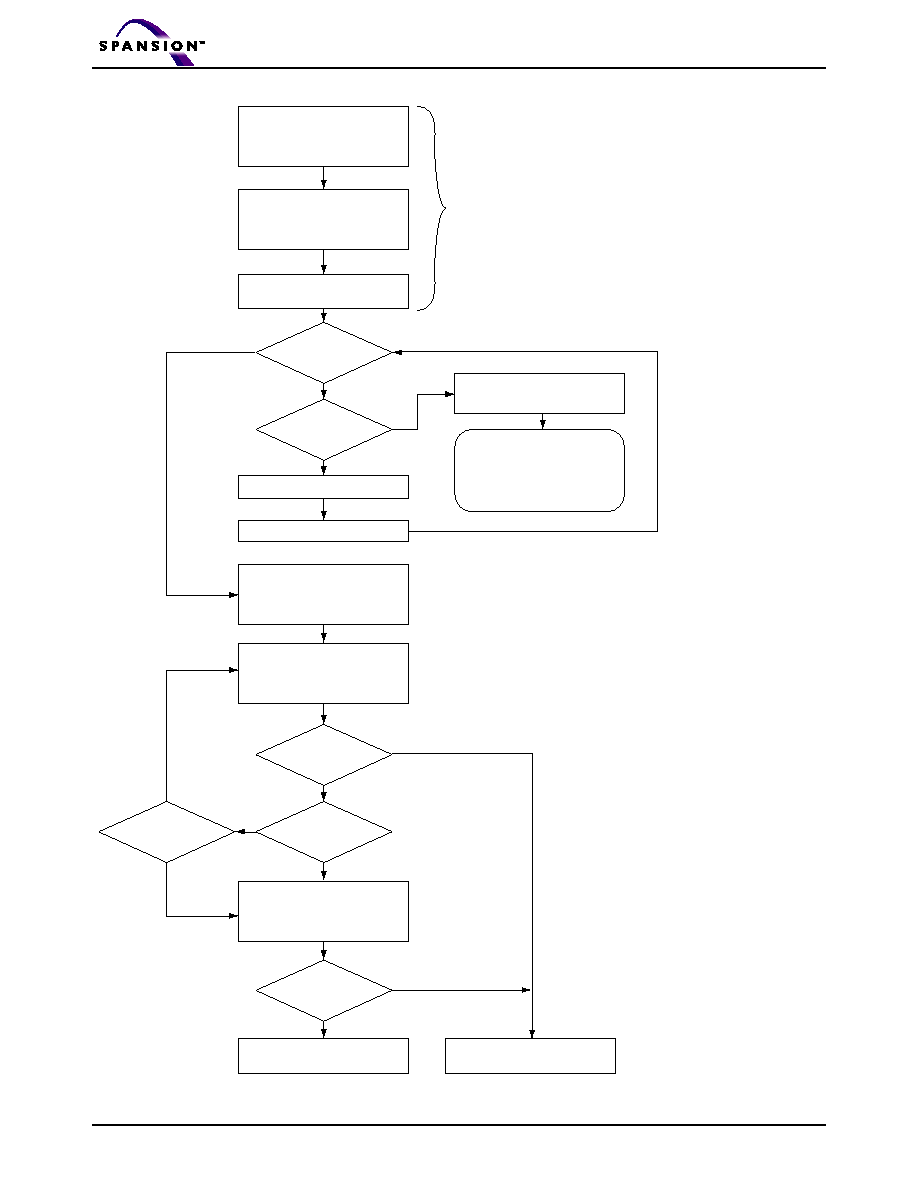
30
S70GL256M00
September 8, 2004
P R E L I M I N A R Y
Figure 4.
Write Buffer Programming Operation
Write "Write to Buffer"
command and
Sector Address
Write number of addresses
to program minus 1(WC)
and Sector Address
Write program buffer to
flash sector address
Write first address/data
Write to a different
sector address
FAIL or ABORT
PASS
Read DQ7 - DQ0 at
Last Loaded Address
Read DQ7 - DQ0 with
address = Last Loaded
Address
Write next address/data pair
WC = WC - 1
WC = 0 ?
Part of "Write to Buffer"
Command Sequence
Yes
Yes
Yes
Yes
Yes
Yes
No
No
No
No
No
No
Abort Write to
Buffer Operation?
DQ7 = Data?
DQ7 = Data?
DQ5 = 1?
DQ1 = 1?
Write to buffer ABORTED.
Must write "Write-to-buffer
Abort Reset" command
sequence to return
to read mode.
Notes:
1.
When Sector Address is specified, any address in
the selected sector is acceptable. However, when
loading Write-Buffer address locations with data, all
addresses must fall within the selected Write-Buffer
Page.
2.
DQ7 and DQ15 may change simultaneously with
DQ5 and DQ13. Therefore, DQ7 and DQ15
should be verified.
3.
If this flowchart location was reached because
DQ5 and DQ13 = "1", then the device FAILED. If
this flowchart location was reached because
DQ1= "1", then the Write to Buffer operation was
ABORTED. In either case, the proper reset
command must be written before the device can
begin another operation. If DQ1 and DQ9 =1,
write the Write-Buffer-Programming-Abort-Reset
command. if DQ5 and DQ13 =1, write the Reset
command.
4.
See Tables
10
and
11
for command sequences
required for write buffer programming.
(Note 3)
(Note 1)
(Note 2)
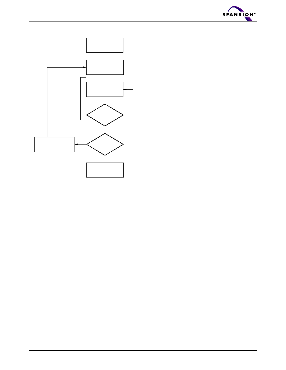
September 8, 2004
S70GL256M00
31
P R E L I M I N A R Y
Figure 5.
Program Operation
Program Suspend/Program Resume
Command Sequence
The Program Suspend command allows the system to
interrupt a programming operation or a Write to Buffer
programming operation so that data can be read from
any non-suspended sector. When the Program Sus-
pend command is written during a programming pro-
cess, the device halts the program operation within 15
µs max (5 µs typical) and updates the status bits. Ad-
dresses are not required when writing the Program
Suspend command.
After the programming operation has been sus-
pended, the system can read array data from any
non-suspended sector. The Program Suspend com-
mand may also be issued during a programming oper-
ation while an erase is suspended. In this case, data
may be read from any addresses not in Erase Sus-
pend or Program Suspend. If a read is needed from
the SecSi Sector area (One-time Program area), then
user must use the proper command sequences to
enter and exit this region.
The system may also write the autoselect command
sequence when the device is in the Program Suspend
mode. The system can read as many autoselect codes
as required. When the device exits the autoselect
mode, the device reverts to the Program Suspend
mode, and is ready for another valid operation. See
Autoselect Command Sequence for more information.
After the Program Resume command is written, the
device reverts to programming. The system can deter-
mine the status of the program operation using the
DQ7 and DQ15 or DQ6 and DQ14 status bits, just as
in the standard program operation. See Write Opera-
tion Status for more information.
The system must write the Program Resume com-
mand (address bits are don't care) to exit the Program
Suspend mode and continue the programming opera-
tion. Further writes of the Resume command are ig-
nored. Another Program Suspend command can be
written after the device has resume programming.
START
Write Program
Command Sequence
Data Poll
from System
Verify Data?
No
Yes
Last Address?
No
Yes
Programming
Completed
Increment Address
Embedded
Program
algorithm
in progress
Note: See Tables
10
and
11
for program command
sequence.
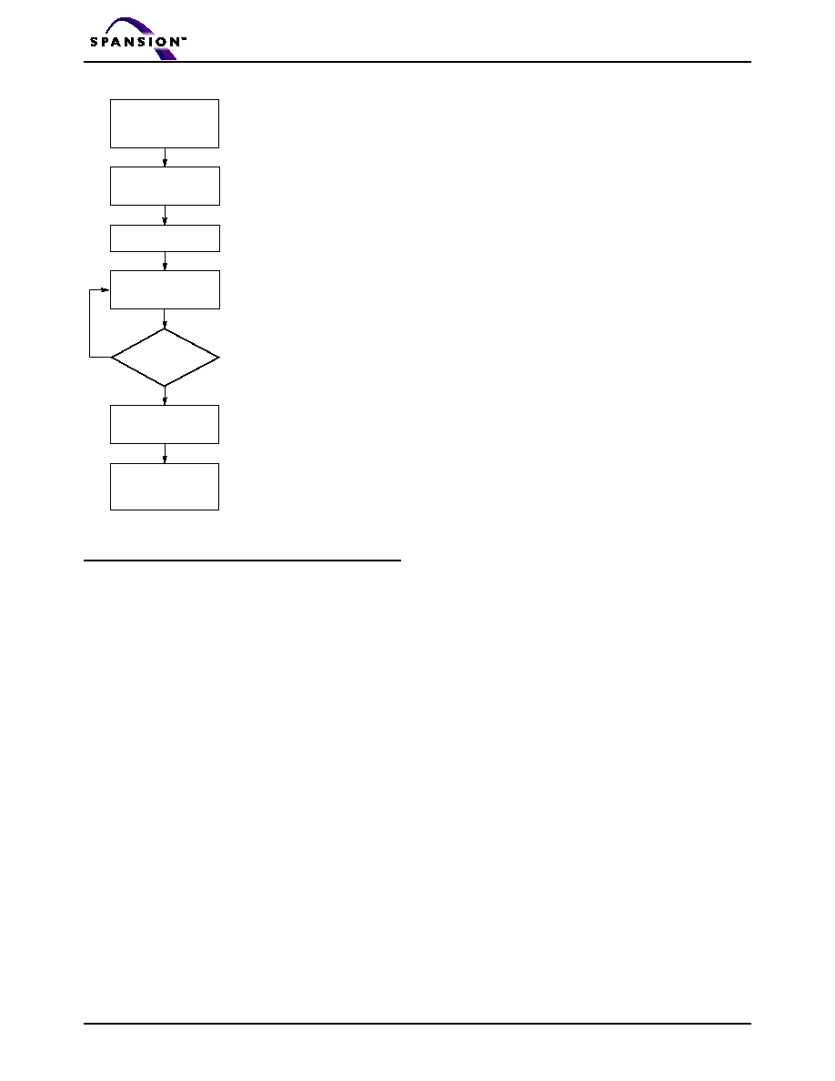
32
S70GL256M00
September 8, 2004
P R E L I M I N A R Y
Figure 6.
Program Suspend/Program Resume
Chip Erase Command Sequence
Chip erase is a six bus cycle operation. The chip erase
command sequence is initiated by writing two unlock
cycles, followed by a set-up command. Two additional
unlock write cycles are then followed by the chip erase
command, which in turn invokes the Embedded Erase
algorithm. The device does
not require the system to
preprogram prior to erase. The Embedded Erase algo-
rithm automatically preprograms and verifies the entire
memory for an all zero data pattern prior to electrical
erase. The system is not required to provide any con-
trols or timings during these operations. Tables
10
and
11
show the address and data requirements for the
chip erase command sequence.
When the Embedded Erase algorithm is complete, the
device returns to the read mode and addresses are no
longer latched. The system can determine the status
of the erase operation by using DQ7 and DQ15, DQ6
and DQ14, or DQ2 and DQ10. Refer to the Write Op-
eration Status section for information on these status
bits.
Any commands written during the chip erase operation
are ignored. However, note that a hardware reset im-
mediately terminates the erase operation. If that oc-
curs, the chip erase command sequence should be
reinitiated once the device has returned to reading
array data, to ensure data integrity.
Note that the
SecSi Sector, autoselect, and CFI functions are un-
available when an program operation is in progress.
Figure 7 illustrates the algorithm for the erase opera-
tion. Refer to the Erase and Program Operations ta-
bles in the AC Characteristics section for parameters,
and Figure 19 section for timing diagrams.
Sector Erase Command Sequence
Sector erase is a six bus cycle operation. The sector
erase command sequence is initiated by writing two
unlock cycles, followed by a set-up command. Two ad-
ditional unlock cycles are written, and are then fol-
lowed by the address of the sector to be erased, and
the sector erase command. Table 11 shows the ad-
dress and data requirements for the sector erase com-
mand sequence.
The device does
not require the system to preprogram
prior to erase. The Embedded Erase algorithm auto-
matically programs and verifies the entire memory for
an all zero data pattern prior to electrical erase. The
system is not required to provide any controls or tim-
ings during these operations.
After the command sequence is written, a sector erase
time-out of 50 µs occurs. During the time-out period,
additional sector addresses and sector erase com-
mands may be written. Loading the sector erase buffer
may be done in any sequence, and the number of sec-
tors may be from one sector to all sectors. The time
between these additional cycles must be less than 50
µs, otherwise erasure may begin. Any sector erase ad-
dress and command following the exceeded time-out
may or may not be accepted. It is recommended that
processor interrupts be disabled during this time to en-
sure all commands are accepted. The interrupts can
be re-enabled after the last Sector Erase command is
written. Any command other than Sector Erase or
Erase Suspend during the time-out period resets
the device to the read mode. The system must re-
write the command sequence and any additional ad-
dresses and commands.
Note that the SecSi Sector,
autoselect, and CFI functions are unavailable when an
erase operation is in progress.
Program Operation
or Write-to-Buffer
Sequence in Progress
Write Program Suspend
Command Sequence
Command is also valid for
Erase-suspended-program
operations
Autoselect and SecSi Sector
read operations are also allowed
Data cannot be read from erase- or
program-suspended sectors
Write Program Resume
Command Sequence
Read data as
required
Done
reading?
No
Yes
Write address/data
XXXh/30h
Device reverts to
operation prior to
Program Suspend
Write address/data
XXXh/B0h
Wait 15 µs
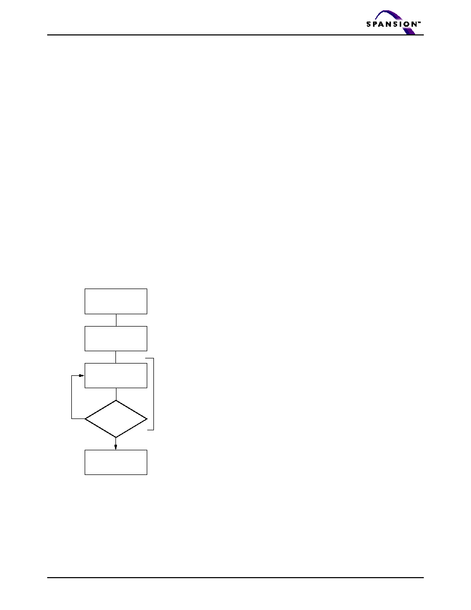
September 8, 2004
S70GL256M00
33
P R E L I M I N A R Y
The system can monitor DQ3 and DQ11 to determine
if the sector erase timer has timed out (See the section
on DQ3 and DQ11: Sector Erase Timer.). The time-out
begins from the rising edge of the final WE# pulse in
the command sequence.
When the Embedded Erase algorithm is complete, the
device returns to reading array data and addresses
are no longer latched. Note that while the Embedded
Erase operation is in progress, the system can read
data from the non-erasing sector. The system can de-
termine the status of the erase operation by reading
DQ7 and DQ15, DQ6 and DQ14, or DQ2 and DQ10 in
the erasing sector. Refer to the Write Operation Status
section for information on these status bits.
Once the sector erase operation has begun, only the
Erase Suspend command is valid. All other com-
mands are ignored. However, note that a hardware
reset immediately terminates the erase operation. If
that occurs, the sector erase command sequence
should be reinitiated once the device has returned to
reading array data, to ensure data integrity.
Figure 7 illustrates the algorithm for the erase opera-
tion. Refer to the Erase and Program Operations ta-
bles in the AC Characteristics section for parameters,
and Figure 19 section for timing diagrams.
Erase Suspend/Erase Resume
Commands
The Erase Suspend command, B0h, allows the sys-
tem to interrupt a sector erase operation and then read
data from, or program data to, any sector not selected
for erasure. This command is valid only during the sec-
tor erase operation, including the 50 µs time-out pe-
riod during the sector erase command sequence. The
Erase Suspend command is ignored if written during
the chip erase operation or Embedded Program
algorithm.
When the Erase Suspend command is written during
the sector erase operation, the device requires a typi-
cal of 5 µs (maximum of 20 µs) to suspend the erase
operation. However, when the Erase Suspend com-
mand is written during the sector erase time-out, the
device immediately terminates the time-out period and
suspends the erase operation.
After the erase operation has been suspended, the
device enters the erase-suspend-read mode. The sys-
tem can read data from or program data to any sector
not selected for erasure. (The device "erase sus-
pends" all sectors selected for erasure.) Reading at
any address within erase-suspended sectors pro-
duces status information on DQ15≠DQ0. The system
can use DQ7 and DQ15, or DQ6 and DQ14 and DQ2
and DQ10 together, to determine if a sector is actively
erasing or is erase-suspended. Refer to the Write Op-
eration Status section for information on these status
bits.
After an erase-suspended program operation is com-
plete, the device returns to the erase-suspend-read
mode. The system can determine the status of the
program operation using the DQ7 and DQ15 or DQ6
and DQ14 status bits, just as in the standard word pro-
gram operation. Refer to the Write Operation Status
section for more information.
In the erase-suspend-read mode, the system can also
issue the autoselect command sequence. Refer to the
Autoselect Mode and Autoselect Command Sequence
sections for details.
To resume the sector erase operation, the system
must write the Erase Resume command. Fur ther
writes of the Resume command are ignored. Another
Erase Suspend command can be written after the chip
has resumed erasing.
START
Write Erase
Command Sequence
(Notes 1, 2)
Data Poll to Erasing
Bank from System
Data = FFh?
No
Yes
Erasure Completed
Embedded
Erase
algorithm
in progress
Figure 7.
Erase Operation
Notes:
1. See Tables
10
and
11
for program command sequence.
2. See the section on DQ3 and DQ10 for information on
the sector erase timer.
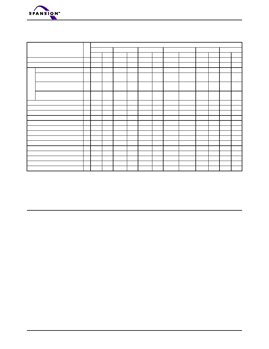
34
S70GL256M00
September 8, 2004
P R E L I M I N A R Y
Command Definitions
Table 10.
Command Definitions (x32 Mode, WORD# = V
IH
)
Legend:
X = Don't care
RA = Read Address of the memory location to be read.
RD = Read Data read from location RA during read operation.
PA = Program Address. Addresses latch on the falling edge of the WE#
or CE# pulse, whichever happens later.
PD = Program Data for location PA. Data latches on the rising edge of
WE# or CE# pulse, whichever happens first.
SA = Sector Address of sector to be verified (in autoselect mode) or
erased. Address bits A22≠A15 uniquely select any sector.
WBL = Write Buffer Location. Address must be within the same write
buffer page as PA.
DWC = Doubleword Count. Number of write buffer locations to load
minus 1.
Notes:
1.
See Table 1 for description of bus operations.
2.
All values are in hexadecimal.
3.
Except for the read cycle and the fourth cycle of the autoselect
command sequence, all bus cycles are write cycles.
4.
Data bits DQ31≠DQ16 are don't care in command sequences,
except for RD, PD and DWC.
5.
Unless otherwise noted, address bits A22≠A11 are don't cares.
6.
No unlock or command cycles required when device is in read
mode.
7.
The Reset command is required to return to the read mode (or to
the erase-suspend-read mode if previously in Erase Suspend)
when the device is in the autoselect mode, or if DQ5 and/or DQ13
goes high while the device is providing status information.
8.
The fourth cycle of the autoselect command sequence is a read
cycle. Data bits DQ31≠DQ16 are don't care. See the Autoselect
Command Sequence section for more information.
9.
The device ID must be read in three cycles.
10. If WP# protects the highest address sector, the data is 9898h for
factory locked and 1818h for not factory locked. If WP# protects
the lowest address sector, the data is 8888h for factory locked
and 0808h for not factor locked.
11. The total number of cycles in the command sequence is
determined by the number of doublewords written to the write
buffer. The maximum number of cycles in the command
sequence is 21.
12. The data is 0000h for an unprotected sector and 0101h for a
protected sector.
13. Command sequence resets device for next command after
aborted write-to-buffer operation.
14. The Unlock Bypass command is required prior to the Unlock
Bypass Program command.
15. The Unlock Bypass Reset command is required to return to the
read mode when the device is in the unlock bypass mode.
16. The system may read and program in non-erasing sectors, or
enter the autoselect mode, when in the Erase Suspend mode.
The Erase Suspend command is valid only during a sector erase
operation.
17. The Erase Resume command is valid only during the Erase
Suspend mode.
18. Command is valid when device is ready to read array data or when
device is in autoselect mode.
Command
Sequence
(Note 1)
Cy
c
l
e
s
Bus Cycles (Notes 2≠5)
First
Second Third
Fourth
Fifth Sixth
Addr
Data
Addr
Data
Addr
Data
Addr
Data
Addr
Data
Addr
Data
Read (Note 6)
1
RA
RD
Reset (Note 7)
1
XXX
F0F0
A
u
t
o
s
e
lec
t
(N
ot
e
8)
Manufacturer ID
4
555
AAAA
2AA
5555
555
9090
X00
00000101
Device ID (Note 9)
6
555
AAAA
2AA
5555
555
9090
X01
22227
E7E
X0E
22221
212
X0F
2222
0000
SecSi
TM
Sector Factory Protect
(Note 10)
4
555
AAAA
2AA
5555
555
9090
X03
(Note 10)
Sector Group Protect Verify
(Note 12)
4
555
AAAA
2AA
5555
555
9090
(SA)X02
0000/010
1
Enter SecSi Sector Region
3
555
AAAA
2AA
5555
555
8888
Exit SecSi Sector Region
4
555
AAAA
2AA
5555
555
9090
XXX
0000
Program
4
555
AAAA
2AA
5555
555
A0A0
PA
PD
Write to Buffer (Note 11)
3
555
AAAA
2AA
5555
SA
2525
SA
DWC
PA
PD
WBL
PD
Program Buffer to Flash
1
SA
2929
Write to Buffer Abort Reset (Note 13)
3
555
AAAA
2AA
5555
555
F0F0
Unlock Bypass
3
555
AAAA
2AA
5555
555
2020
Unlock Bypass Program (Note 14)
2
XXX
A0A0
PA
PD
Unlock Bypass Reset (Note 15)
2
XXX
9090
XXX
0000
Chip Erase
6
555
AAAA
2AA
5555
555
8080
555
AAAA
2AA
5555
555
1010
Sector Erase
6
555
AAAA
2AA
5555
555
8080
555
AAAA
2AA
5555
SA
3030
Program/Erase Suspend (Note 16)
1
XXX
B0B0
Program/Erase Resume (Note 17)
1
XXX
3030
CFI Query (Note 18)
1
55
9898
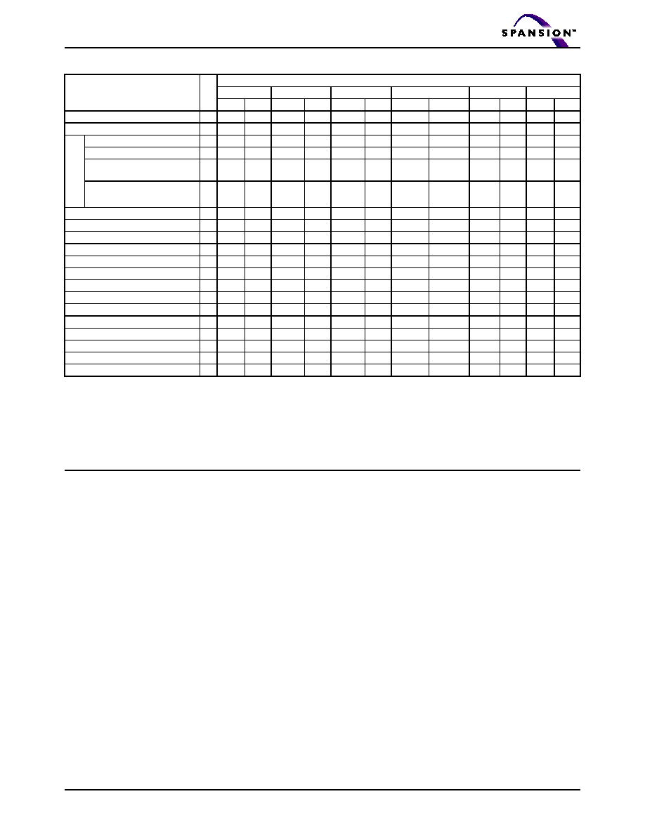
September 8, 2004
S70GL256M00
35
P R E L I M I N A R Y
Table 11.
Command Definitions (x16 Mode, WORD# = V
IL
)
Legend:
X = Don't care
RA = Read Address of the memory location to be read.
RD = Read Data read from location RA during read operation.
PA = Program Address. Addresses latch on the falling edge of the WE#
or CE# pulse, whichever happens later.
PD = Program Data for location PA. Data latches on the rising edge of
WE# or CE# pulse, whichever happens first.
SA = Sector Address of sector to be verified (in autoselect mode) or
erased. Address bits A22≠A15 uniquely select any sector.
WBL = Write Buffer Location. Address must be within the same write
buffer page as PA.
WC = Word Count. Number of write buffer locations to load minus 1.
Notes:
1.
See Table 1 for description of bus operations.
2.
All values are in hexadecimal.
3.
Except for the read cycle and the fourth cycle of the autoselect
command sequence, all bus cycles are write cycles.
4.
Data bits DQ31≠DQ15 are don't care in command sequences.
5.
Unless otherwise noted, address bits A22≠A11 are don't cares.
6.
No unlock or command cycles required when device is in read
mode.
7.
The Reset command is required to return to the read mode (or to
the erase-suspend-read mode if previously in Erase Suspend)
when the device is in the autoselect mode, or if DQ5 and/or
DQ13goes high while the device is providing status information.
8.
The fourth cycle of the autoselect command sequence is a read
cycle. Data bits DQ31≠DQ16 are don't care. See the Autoselect
Command Sequence section for more information.
9.
The device ID must be read in three cycles.
10. If WP# protects the highest address sector, the data is 9898h for
factory locked and 1818h for not factory locked. If WP# protects
the lowest address sector, the data is 8888h for factory locked
and 0808h for not factor locked.
11. The total number of cycles in the command sequence is
determined by the number of words written to the write buffer. The
maximum number of cycles in the command sequence is 37.
12. The data is 0000h for an unprotected sector group and 0101h for
a protected sector group.
13. Command sequence resets device for next command after
aborted write-to-buffer operation.
14. The Unlock Bypass command is required prior to the Unlock
Bypass Program command.
15. The Unlock Bypass Reset command is required to return to the
read mode when the device is in the unlock bypass mode.
16. The system may read and program in non-erasing sectors, or
enter the autoselect mode, when in the Erase Suspend mode.
The Erase Suspend command is valid only during a sector erase
operation.
17. The Erase Resume command is valid only during the Erase
Suspend mode.
18. Command is valid when device is ready to read array data or when
device is in autoselect mode.
Command
Sequence
(Note 1)
Cy
c
l
e
s
Bus Cycles (Notes 2≠5)
First
Second Third
Fourth
Fifth Sixth
Addr
Data
Addr
Data
Addr
Data
Addr
Data
Addr
Data
Addr
Data
Read (Note 6)
1
RA
RD
Reset (Note 7)
1
XXX
F0F0
A
u
t
o
s
e
lec
t
(N
ot
e
8
)
Manufacturer ID
4
AAA
AAAA
555
5555
AAA
9090
X00
0101
Device ID (Note 9)
6
AAA
AAAA
555
5555
AAA
9090
X02
7E7E
X1C
1212
X1E
0000
SecSi
TM
Sector Factory Protect
(Note 10)
4
AAA
AAAA
555
5555
AAA
9090
X06
(Note 10)
Sector Group Protect Verify
(Note 12)
4
AAA
AAAA
555
5555
AAA
9090
(SA)X04
0000/010
1
Enter SecSi Sector Region
3
AAA
AAAA
555
5555
AAA
8888
Exit SecSi Sector Region
4
AAA
AAAA
555
5555
AAA
9090
XXX
0000
Program
4
AAA
AAAA
555
5555
AAA
A0A0
PA
PD
Write to Buffer (Note 11)
3
AAA
AAAA
555
5555
SA
2525
SA
WC
PA
PD
WBL
PD
Program Buffer to Flash
1
SA
2929
Write to Buffer Abort Reset (Note 13)
3
AAA
AAAA
555
5555
AAA
F0F0
Unlock Bypass
3
AAA
AAAA
555
5555
AAA
2020
Unlock Bypass Program (Note 14)
2
XXX
A0A0
PA
PD
Unlock Bypass Reset (Note 15)
2
XXX
9090
XXX
0000
Chip Erase
6
AAA
AAAA
555
5555
AAA
8080
AAA
AAAA
555
5555
AAA
1010
Sector Erase
6
AAA
AAAA
555
5555
AAA
8080
AAA
AAAA
555
5555
SA
3030
Program/Erase Suspend (Note 16)
1
XXX
B0B0
Program/Erase Resume (Note 17)
1
XXX
3030
CFI Query (Note 18)
1
AA
9898
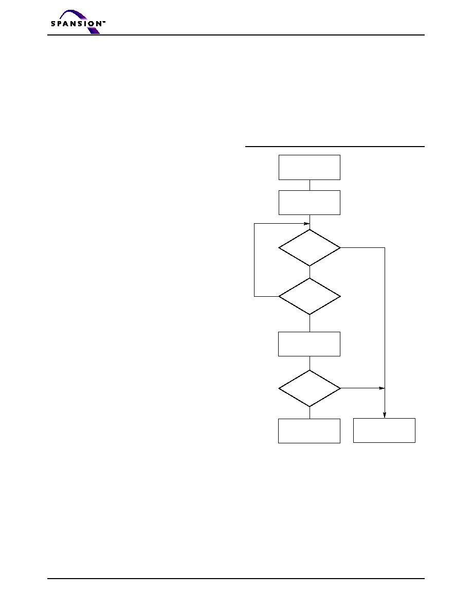
36
S70GL256M00
September 8, 2004
P R E L I M I N A R Y
WRITE OPERATION STATUS
The device provides several bits to determine the status of a
program or erase operation: DQ2 and DQ10, DQ3 and
DQ11, DQ5 and DQ13, DQ6 and DQ14, and DQ7 and
DQ15. Table 12 and the following subsections describe the
function of these bits. DQ7 and DQ15 and DQ6 and DQ14
each offer a method for determining whether a program or
erase operation is complete or in progress. The device
also provides a ha rdware-b ase d output sign al,
RY/BY#, to determine whether an Embedded Program
or Erase operation is in progress or has been com-
pleted.
DQ7 and DQ5: Data# Polling
The Data# Polling bit, DQ7 and DQ15, indicates to the host
system whether an Embedded Program or Erase algorithm
is in progress or completed, or whether the device is in
Erase Suspend. Data# Polling is valid after the rising edge
of the final WE# pulse in the command sequence.
During the Embedded Program algorithm, the device out-
puts on DQ7 and DQ15 the complement of the datum pro-
grammed to DQ7 and DQ15. This DQ7 and DQ15 status
also applies to programming during Erase Suspend. When
the Embedded Program algorithm is complete, the device
outputs the datum programmed to DQ7 and DQ15. The
system must provide the program address to read valid sta-
tus information on DQ7 and DQ15. If a program address
falls within a protected sector, Data# Polling on DQ7 and
DQ15 is active for approximately 1 µs, then the device re-
turns to the read mode.
During the Embedded Erase algorithm, Data# Polling
produces a "0" on DQ7 and DQ15. When the Embed-
ded Erase algorithm is complete, or if the device en-
ters the Erase Suspend mode, Data# Polling produces
a "1" on DQ7 and DQ15. The system must provide an
address within any of the sectors selected for erasure
to read valid status information on DQ7 and DQ15.
After an erase command sequence is written, if all
sectors selected for erasing are protected, Data# Poll-
ing on DQ7 and DQ15 is active for approximately 100
µs, then the device returns to the read mode. If not all
selected sectors are protected, the Embedded Erase
algorithm erases the unprotected sectors, and ignores
the selected sectors that are protected. However, if the
system reads DQ7 and DQ15 at an address within a
protected sector, the status may not be valid.
Just prior to the completion of an Embedded Program
or Erase operation, DQ7 and DQ15 may change asyn-
chronously with DQ6≠DQ0 and DQ14≠DQ8 while Out-
put Enable (OE#) is asserted low. That is, the device
may change from providing status information to valid
data on DQ7 and DQ15. Depending on when the sys-
tem samples the DQ7 and DQ15 output, it may read
the status or valid data. Even if the device has com-
pleted the program or erase operation and DQ7 has
val i d d at a, th e d a ta o u tpu ts o n D Q 6 ≠D Q 0 a n d
D Q 1 4 ≠ D Q 8 may b e s ti ll i nva lid . Va l id d a t a o n
DQ15≠DQ0 will appear on successive read cycles.
Table 12 shows the outputs for Data# Polling on DQ7
and DQ15. Figure 8 shows the Data# Polling algo-
rithm. Figure 20 in the AC Characteristics section
shows the Data# Polling timing diagram.
Figure 8.
Data# Polling Algorithm
DQ7 = Data?
Yes
No
No
DQ5 = 1?
No
Yes
Yes
FAIL
PASS
Read DQ7≠DQ0
Addr = VA
Read DQ7≠DQ0
Addr = VA
DQ7 = Data?
START
Notes:
1. VA = Valid address for programming. During a sector
erase operation, a valid address is any sector address
within the sector being erased. During chip erase, a
valid address is any non-protected sector address.
2. DQ7 and DQ15 should be rechecked even if DQ5
and/or DQ13 = "1" because DQ7 and DQ15 may
change simultaneously with DQ5 and DQ13.

September 8, 2004
S70GL256M00
37
P R E L I M I N A R Y
RY/BY#: Ready/Busy#
The RY/BY# is a dedicated, open-drain output pin
which indicates whether an Embedded Algorithm is in
progress or complete. The RY/BY# status is valid after
the rising edge of the final WE# pulse in the command
sequence. Since RY/BY# is an open-drain output, sev-
eral RY/BY# pins can be tied together in parallel with a
pull-up resistor to V
CC
.
If the output is low (Busy), the device is actively eras-
ing or programming. (This includes programming in
the Erase Suspend mode.) If the output is high
(Ready), the device is in the read mode, the standby
mode, or in the erase-suspend-read mode. Table 12
shows the outputs for RY/BY#.
DQ6 and DQ14: Toggle Bits I
Toggle Bit I on DQ6 and DQ14indicates whether an
Embedded Program or Erase algorithm is in progress
or complete, or whether the device has entered the
Erase Suspend mode. Toggle Bit I may be read at any
address, and is valid after the rising edge of the final
WE# pulse in the command sequence (prior to the
program or erase operation), and during the sector
erase time-out.
During an Embedded Program or Erase algorithm op-
eration, successive read cycles to any address cause
DQ6 and DQ14 to toggle. The system may use either
OE# or CE# to control the read cycles. When the oper-
ation is complete, DQ6 and DQ14 stops toggling.
After an erase command sequence is written, if all sectors
selected for erasing are protected, DQ6 and DQ14 toggles
for approximately 100 µs, then returns to reading array data.
If not all selected sectors are protected, the Embedded
Erase algorithm erases the unprotected sectors, and ig-
nores the selected sectors that are protected.
The system can use DQ6 and DQ14 and DQ2 and DQ10
together to determine whether a sector is actively erasing or
is erase-suspended. When the device is actively erasing
(that is, the Embedded Erase algorithm is in progress), DQ6
and DQ14 toggle. When the device enters the Erase Sus-
pend mode, DQ6 and DQ14 stop toggling. However, the
system must also use DQ2 and DQ10 to determine which
sectors are erasing or erase-suspended. Alternatively, the
system can use DQ7 and DQ15 (see the subsection on
DQ7 and DQ15: Data# Polling).
If a program address falls within a protected sector,
DQ6 and DQ14 toggle for approximately 1 µs after the
program command sequence is written, then returns
to reading array data.
DQ6 and DQ14 also toggle during the erase-sus-
pend-program mode, and stops toggling once the Em-
bedded Program algorithm is complete.
Table 12 shows the outputs for Toggle Bit I on DQ6
and DQ14. Figure 9 shows the toggle bit algorithm.
Figure 21 in the "AC Characteristics" section shows
the toggle bit timing diagrams. Figure 22 shows the dif-
ferences between DQ2 and DQ10 and DQ6 and DQ14
in graphical form. See also the subsection on DQ2 and
DQ10: Toggle Bits II.

38
S70GL256M00
September 8, 2004
P R E L I M I N A R Y
Figure 9.
Toggle Bit Algorithm
DQ2 and DQ10: Toggle Bits II
The "Toggle Bits II" on DQ2 and DQ10, when used
with DQ6 and DQ14, indicate whether a particular
sector is actively erasing (that is, the Embedded Erase
algorithm is in progress), or whether that sector is
erase-suspended. Toggle Bits II are valid after the ris-
ing edge of the final WE# pulse in the command se-
quence.
DQ2 and DQ10 toggle when the system reads at ad-
dresses within those sectors that have been selected
for erasure. (The system may use either OE# or CE#
to control the read cycles.) But DQ2 and DQ10 cannot
distinguish whether the sector is actively erasing or is
erase-suspended. DQ6 and DQ14, by comparison, in-
dicate whether the device is actively erasing, or is in
Erase Suspend, but cannot distinguish which sectors
are selected for erasure. Thus, both status bits are re-
quired for sector and mode information. Refer to Table
12 to compare outputs for DQ2 and DQ10 and DQ6
and DQ14.
Figure 9 shows the toggle bit algorithm in flowchart
form, and the section "DQ2 and DQ10: Toggle Bits II"
ex p l a i n s t h e a l g o r i t h m . S e e a l so t h e RY /B Y # :
Ready/Busy# subsection. Figure 21 shows the toggle
bit timing diagram. Figure 22 shows the differences
between DQ2 and DQ10 and DQ6 and DQ14 in
graphical form.
Reading Toggle Bits DQ6 and DQ14/DQ2
and DQ10
Refer to Figure 9 for the following discussion. When-
ever the system initially begins reading toggle bits sta-
tus, it must read DQ15≠DQ0 at least twice in a row to
determine whether a toggle bit is toggling. Typically,
the system would note and store the value of the tog-
gle bit after the first read. After the second read, the
system would compare the new value of the toggle bit
with the first. If the toggle bits are not toggling, the de-
vice has completed the program or erase operation.
The system can read array data on DQ15≠DQ0 on the
following read cycle.
However, if after the initial two read cycles, the system
determines that one of the toggle bits are still toggling,
the system also should note whether the value of DQ5
and DQ13 is high (see the section on DQ5 and DQ13).
If it is, the system should then deter mine again
whether the toggle bit is toggling, since the toggle bit
may have stopped toggling just as DQ5 and/or DQ13
went high. If the toggle bits are no longer toggling, the
device has successfully completed the program or
erase operation. If it is still toggling, the device did not
completed the operation successfully, and the system
must write the reset command to return to reading
array data.
START
No
Yes
Yes
DQ5 = 1?
No
Yes
Toggle Bit
= Toggle?
No
Program/Erase
Operation Not
Complete, Write
Reset Command
Program/Erase
Operation Complete
Read DQ7≠DQ0
Toggle Bit
= Toggle?
Read DQ7≠DQ0
Twice
Read DQ7≠DQ0
Note: The system should recheck the toggle bit even if
DQ5 and DQ13= "1" because the toggle bit may stop
toggling as DQ5 and DQ13 changes to "1." See the
subsections on DQ6 and DQ14 and DQ2 and DQ10 for
more information.

September 8, 2004
S70GL256M00
39
P R E L I M I N A R Y
The remaining scenario is that the system initially de-
termines that the toggle bit is toggling and DQ5 and/or
DQ13 has not gone high. The system may continue to
monitor the toggle bits and DQ5 and DQ13 through
successive read cycles, determining the status as de-
scribed in the previous paragraph. Alternatively, it may
choose to perform other system tasks. In this case, the
system must start at the beginning of the algorithm
when it returns to determine the status of the opera-
tion (top of Figure 9).
DQ5 and DQ13: Exceeded Timing Limits
D Q 5 i nd ic ate s w he th er th e p ro gram , e ra se, o r
write-to-buffer time has exceeded a specified internal
pulse count limit. Under these conditions DQ5 and DQ13
produce a "1," indicating that the program or erase cycle
was not successfully completed.
The device may output a "1" on DQ5 and/or DQ13 if
the system tries to program a "1" to a location that was
previously programmed to "0." Only an erase opera-
tion can change a "0" back to a "1." Under this con-
dition, the device halts the operation, and when the
timing limit has been exceeded, DQ5 and/or DQ13
produces a "1."
In all these cases, the system must write the reset
command to return the device to the reading the array
(or to erase-suspend-read if the device was previously
in the erase-suspend-program mode).
DQ3 and DQ11: Sector Erase Timer
After writing a sector erase command sequence, the
system may rea d DQ3 and DQ 11 to de ter min e
whether or not erasure has begun. (The sector erase
timer does not apply to the chip erase command.) If
additional sectors are selected for erasure, the entire
time-out also applies after each additional sector
erase command. When the time-out period is com-
plete, DQ3 and DQ11 switch from a "0" to a "1." If the
time between additional sector erase commands from
the system can be assumed to be less than 50 µs, the
system need not monitor DQ3 and DQ11. See also the
Sector Erase Command Sequence section.
After the sector erase command is written, the system
should read the status of DQ7 and DQ15 (Data# Poll-
ing) or DQ6 and DQ14 (Toggle Bits I) to ensure that
the device has accepted the command sequence, and
then read DQ3 and DQ11. If DQ3 and DQ11 are "1,"
the Embedded Erase algorithm has begun; all further
commands (except Erase Suspend) are ignored until
the erase operation is complete. If DQ3 and DQ11 are
"0," the device will accept additional sector erase com-
mands. To ensure the command has been accepted,
the system software should check the status of DQ3
and DQ11 prior to and following each subsequent sec-
tor erase command. If DQ3 and DQ11 are high on the
second status check, the last command might not
have been accepted.
Table 12 shows the status of DQ3 and DQ11 relative
to the other status bits.

40
S70GL256M00
September 8, 2004
P R E L I M I N A R Y
DQ1: Write-to-Buffer Abort
DQ1 indicates whether a Write-to-Buffer operation
was aborted. Under these conditions DQ1 and DQ9
p r o d u c e a " 1 " . T h e s y s t e m m u s t i s s u e t h e
Write-to-Buffer-Abort-Reset command sequence to re-
turn the device to reading array data. See Write Buffer
Programming section for more details.
Table 12.
Write Operation Status
Notes:
1. DQ5 and DQ13 switch to `1' when an Embedded Program, Embedded Erase, or Write-to-Buffer operation has exceeded the
maximum timing limits. Refer to the section on DQ5 and DQ13 for more information.
2. DQ7 and DQ15 and DQ2 and DQ10 require a valid address when reading status information. Refer to the appropriate subsection
for further details.
3. The Data# Polling algorithm should be used to monitor the last loaded write-buffer address location.
4. DQ1 and DQ9 switch to `1' when the device has aborted the write-to-buffer operation.
Status
DQ7/DQ15
(Note 2)
DQ6/DQ14
DQ5/
DA13
(Note 1)
DQ3/
DQ11
DQ2/DQ10
(Note 2)
DQ1/
DQ9
RY/BY#
Standard
Mode
Embedded Program Algorithm
DQ7/DA15#
Toggle
0
N/A
No toggle
0
0
Embedded Erase Algorithm
0
Toggle
0
1
Toggle
N/A
0
Program
Suspend
Mode
Program-
Suspend
Read
Program-Suspended
Sector
Invalid (not allowed)
1
Non-Program
Suspended Sector
Data
1
Erase
Suspend
Mode
Erase-
Suspend
Read
Erase-Suspended
Sector
1
No toggle
0
N/A
Toggle
N/A
1
Non-Erase
Suspended Sector
Data
1
Erase-Suspend-Program
(Embedded Program)
DQ7/DQ15#
Toggle
0
N/A
N/A
N/A
0
Write-to-
Buffer
Busy (Note 3)
DQ7/DQ15#
Toggle
0
N/A
N/A
0
0
Abort (Note 4)
DQ7/DQ15#
Toggle
0
N/A
N/A
1
0
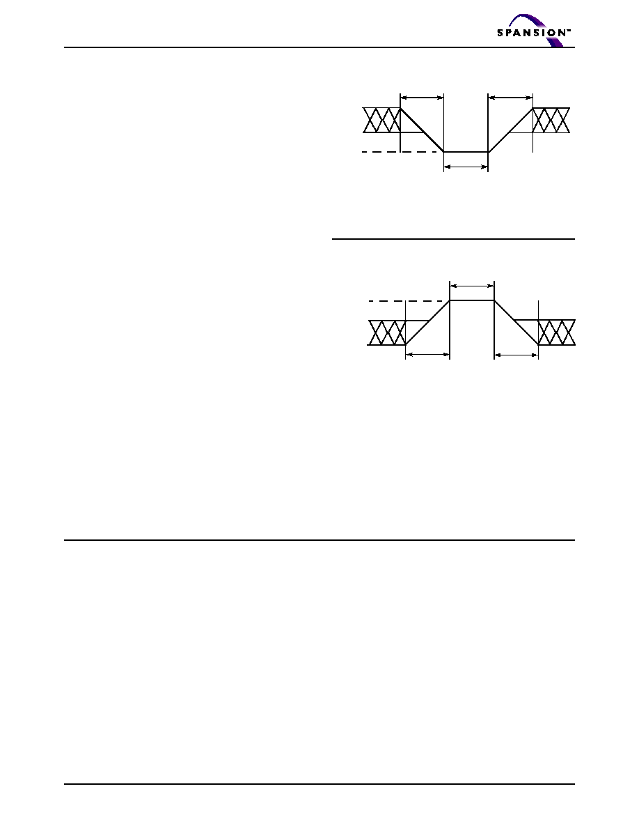
September 8, 2004
S70GL256M00
41
P R E L I M I N A R Y
ABSOLUTE MAXIMUM RATINGS
Storage Temperature
Plastic Packages . . . . . . . . . . . . . . . ≠65∞C to +150∞C
Ambient Temperature
with Power Applied. . . . . . . . . . . . . . ≠65∞C to +125∞C
Voltage with Respect to Ground
V
CC
(Note 1) . . . . . . . . . . . . . . . . . ≠0.5 V to +4.0 V
A9, OE#, WP#/ACC, and RESET#
(Note 2) . . . . . . . . . . . . . . . . . . . . ≠0.5 V to +12.5 V
All other pins (Note 1) . . . . . . ≠0.5 V to V
CC
+0.5 V
Output Short Circuit Current (Note 3) . . . . . . 200 mA
Notes:
1. Minimum DC voltage on input or I/O pins is ≠0.5 V.
Dur in g vo ltage tran sitions, inpu t or I/O pins may
overshoot V
SS
to ≠2.0 V for periods of up to 20 ns.
Maximum DC voltage on input or I/O pins is V
CC
+0.5 V.
See Figure 10. During voltage transitions, input or I/O
pins may overshoot to V
CC
+2.0 V for periods up to 20 ns.
See Figure 11.
2. Minimum DC input voltage on pins A9, OE#, ACC, and
RESET# is ≠0.5 V. During voltage transitions, A9, OE#,
WP#/ACC, and RESET# may overshoot V
SS
to ≠2.0 V for
periods of up to 20 ns. See Figure 10. Maximum DC
input voltage on pin A9, OE#, WP#/ACC, and RESET# is
+12.5 V which may overshoot to +14.0 V for periods up
to 20 ns.
3. No more than one output may be shorted to ground at a
time. Duration of the short circuit should not be greater
than one second.
Stresses above those listed under "Absolute Maximum
Ratings" may cause permanent damage to the device. This
is a stress rating only; functional operation of the device at
these or any other conditions above those indicated in the
operational sections of this data sheet is not implied.
Ex posure of the d evice to absolute m aximum rating
conditions for extended periods may affect device reliability.
OPERATING RANGES
Industrial (I) Devices
Ambient Temperature (T
A
) . . . . . . . . . ≠40∞C to +85∞C
Supply Voltages
V
CC
. . . . . . . . . . . . . . . . . . . . . . . . . . . . . . . 3.0≠3.6 V
V
IO
(Note 5)
. . . . . . . . . . . . . . . . . . . . . . . . . 1.65≠3.6 V
4. Operating ranges define those limits between which the
functionality of the device is guaranteed.
5. See ordering information for valid V
CC
/V
IO
combinations.
The I/Os will not operate at 3 V when V
IO
= 1.8 V
20 ns
20 ns
+0.8 V
≠0.5 V
20 ns
≠2.0 V
Figure 10.
Maximum Negative
Overshoot Waveform
20 ns
20 ns
V
CC
+2.0 V
V
CC
+0.5 V
20 ns
2.0 V
Figure 11.
Maximum Positive
Overshoot Waveform
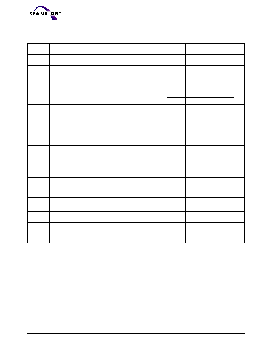
42
S70GL256M00
September 8, 2004
P R E L I M I N A R Y
DC CHARACTERISTICS
CMOS Compatible
Notes:
1.
On the WP#/ACC pin only, the maximum input load current when
WP# = V
IL
is ± 5.0 µA.
2.
The I
CC
current listed is typically less than 2 mA/MHz, with OE# at
V
IH
.
3.
Maximum I
CC
specifications are tested with V
CC
= V
CC
max.
4.
I
CC
active while Embedded Erase or Embedded Program is in
progress.
5.
Automatic sleep mode enables the low power mode when
addresses remain stable for t
ACC
+ 30 ns.
6.
If V
IO
< V
CC
, maximum V
IL
for CE# and DQ I/Os is 0.3 V
IO
.
Maximum V
IH
for these connections is V
IO
+ 0.3 V
7.
V
CC
voltage requirements.
8.
V
IO
voltage requirements.
9.
Not 100% tested.
Parameter
Symbol
Parameter Description
(Notes)
Test Conditions
Min
Typ
Max
Unit
I
LI
Input Load Current (1)
V
IN
= V
SS
to V
CC
,
V
CC
= V
CC
max
±2.0
µA
I
LIT
A9, ACC Input Load Current
V
CC
= V
CC max
; A9 = 12.5 V
70
µA
I
LR
Reset Leakage Current
V
CC
= V
CC max
; RESET# = 12.5 V
35
µA
I
LO
Output Leakage Current
V
OUT
= V
SS
to V
CC
,
V
CC
= V
CC max
±2.0
µA
I
CC1
V
CC
Active Read Current (2, 3)
CE# = V
IL,
OE# = V
IH
,
1 MHz
6
68
mA
5 MHz
26
86
I
CC2
V
CC
Initial Page Read Current (2, 3)
CE# = V
IL,
OE# = V
IH
1 MHz
8
100
10 MHz
80
160
mA
I
CC3
V
CC
Intra-Page Read Current (2, 3)
CE# = V
IL,
OE# = V
IH
10 MHz
6
40
33 MHz
12
80
mA
I
CC4
V
CC
Active Write Current (3, 4)
CE# = V
IL,
OE# = V
IH
100
120
mA
I
CC5
V
CC
Standby Current (3)
CE#, RESET# = V
CC
± 0.3 V, WP# = V
IH
2
10
µA
I
CC6
V
CC
Reset Current (3)
RESET# = V
SS
± 0.3 V, WP# = V
IH
2
10
µA
I
CC7
Automatic Sleep Mode (3, 5)
V
IH
= V
CC
± 0.3 V; V
IL
= V
SS
± 0.3 V,
WP# = V
IH
2
10
µA
I
ACC
ACC Accelerated Program Current (3)
CE# = V
IL
, OE# = V
IH
ACC pin
20
40
mA
V
CC
pin
60
120
mA
V
IL1
Input Low Voltage 1 (6, 7)
≠0.5
0.8
V
V
IH1
Input High Voltage 1 (6, 7)
1.9
V
CC
+ 0.5
V
V
IL2
Input Low Voltage 2 (6, 8)
≠0.5
0.3 x V
IO
V
V
IH2
Input High Voltage 2 (6, 8)
1.9
V
IO
+ 0.5
V
V
HH
Voltage for ACC Program Acceleration
V
CC
= 2.7 ≠3.6 V
11.5
12.5
V
V
ID
Voltage for Autoselect and Temporary
Sector Unprotect
V
CC
= 2.7 ≠3.6 V
11.5
12.5
V
V
OH1
Output High Voltage
I
OH
= ≠2.0 mA, V
CC
= V
CC min
= V
IO
0.85 V
IO
V
V
OH2
I
OH
= ≠100 µA, V
CC
= V
CC min
= V
IO
V
IO
≠0.4
V
V
LKO
Low V
CC
Lock-Out Voltage (6)
2.3
2.5
V
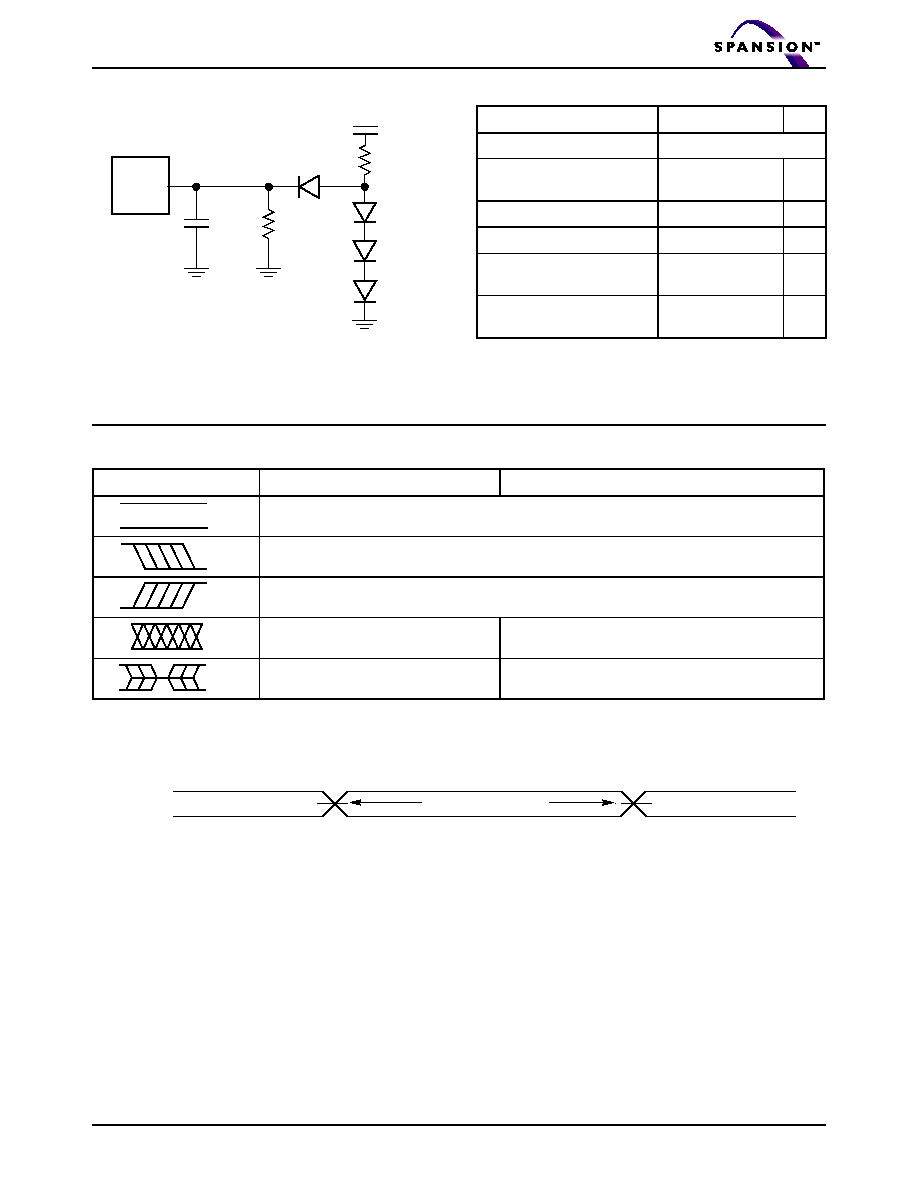
September 8, 2004
S70GL256M00
43
P R E L I M I N A R Y
TEST CONDITIONS
Table 13.
Test Specifications
KEY TO SWITCHING WAVEFORMS
2.7 k
C
L
6.2 k
3.3 V
Device
Under
Test
Note:
Diodes are IN3064 or equivalent.
Figure 12.
Test Setup
Test Condition
All Speeds
Unit
Output Load
1 TTL gate
Output Load Capacitance, C
L
(including jig capacitance)
30
pF
Input Rise and Fall Times
5
ns
Input Pulse Levels
0.0≠3.0
V
Input timing measurement
reference levels (See Note)
1.5 V
Output timing measurement
reference levels
0.5 V
IO
V
WAVEFORM
INPUTS
OUTPUTS
Steady
Changing from H to L
Changing from L to H
Don't Care, Any Change Permitted
Changing, State Unknown
Does Not Apply
Center Line is High Impedance State (High Z)
3.0 V
0.0 V
1.5 V
0.5 V
IO
V
Output
Measurement Level
Input
Figure 13.
Input Waveforms and
Measurement Levels
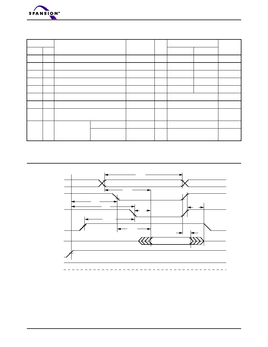
44
S70GL256M00
September 8, 2004
P R E L I M I N A R Y
AC CHARACTERISTICS
Read-Only Operations
Notes:
1. Not 100% tested.
2. See Figure 12 and Table 13 for test specifications
3. AC specifications listed are tested with V
IO
= V
CC
. Contact Spansion for information on AC operation when V
IO
V
CC
.
Parameter
Description
Test Setup
Speed Options
JEDEC
Std.
110R
120R
Unit
t
AVAV
t
RC
Read Cycle Time (Note 1)
Min
110
120
ns
t
AVQV
t
ACC
Address to Output Delay
CE#, OE# = V
IL
Max
110
120
ns
t
ELQV
t
CE
Chip Enable to Output Delay
OE# = V
IL
Max
110
120
ns
t
PACC
Page Access Time
Max
30
30
ns
t
GLQV
t
OE
Output Enable to Output Delay
Max
30
30
ns
t
EHQZ
t
DF
Chip Enable to Output High Z (Note 1)
Max
25
ns
t
GHQZ
t
DF
Output Enable to Output High Z (Note 1)
Max
25
ns
t
AXQX
t
OH
Output Hold Time From Addresses, CE#
or OE#, Whichever Occurs First
Min
0
ns
t
OEH
Output Enable Hold
Time (Note 1)
Read
Min
0
ns
Toggle and
Data# Polling
Min
10
ns
t
OH
t
CE
Outputs
WE#
Addresses
CE#
OE#
HIGH Z
Output Valid
HIGH Z
Addresses Stable
t
RC
t
ACC
t
OEH
t
RH
t
OE
t
RH
0 V
RY/BY#
RESET#
t
DF
Figure 14.
Read Operation Timings
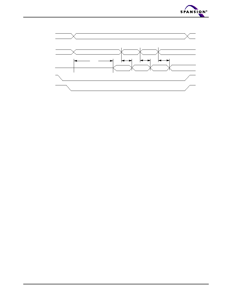
September 8, 2004
S70GL256M00
45
P R E L I M I N A R Y
AC CHARACTERISTICS
* Figure shows doubleword mode. Addresses are A1≠A-1 for word mode.
Figure 15.
Page Read Timings
A20-A2
CE#
OE#
A1-A0*
Data Bus
Same Page
Aa
Ab
Ac
Ad
Qa
Qb
Qc
Qd
t
ACC
t
PACC
t
PACC
t
PACC
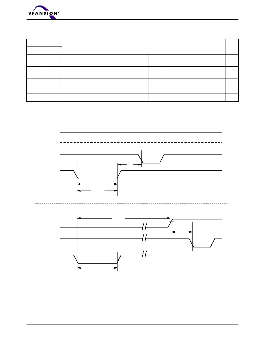
46
S70GL256M00
September 8, 2004
P R E L I M I N A R Y
AC CHARACTERISTICS
Hardware Reset (RESET#)
Note:
1. Not 100% tested.
2. AC specifications listed are tested with V
IO
= V
CC
. Contact Spansion for information on AC operation when V
IO
V
CC
.
Parameter
Description
All Speed Options
Unit
JEDEC
Std.
t
Ready
RESET# Pin Low (During Embedded Algorithms)
to Read Mode (See Note)
Max
20
µs
t
Ready
RESET# Pin Low (NOT During Embedded
Algorithms) to Read Mode (See Note)
Max
500
ns
t
RP
RESET# Pulse Width
Min
500
ns
t
RH
Reset High Time Before Read (See Note)
Min
50
ns
t
RPD
RESET# Low to Standby Mode
Min
20
µs
RESET#
RY/BY#
RY/BY#
t
RP
t
Ready
Reset Timings NOT during Embedded Algorithms
t
Ready
CE#, OE#
t
RH
CE#, OE#
Reset Timings during Embedded Algorithms
RESET#
t
RP
t
RB
Figure 16.
Reset Timings
September 8, 2004
S70GL256M00
47
P R E L I M I N A R Y
AC CHARACTERISTICS
Erase and Program Operations
Notes:
1. Not 100% tested.
2. See the "Erase And Programming Performance" section for more information.
3. For 1≠16 doublewords/1≠32 words programmed.
4. Effective write buffer specification is based upon a 16-doubleword/32-word write buffer operation.
5. AC specifications listed are tested with V
IO
= V
CC
. Contact Spansion for information on AC operation when V
IO
V
CC.
Parameter
Speed Options
JEDEC
Std.
Description
110R
120R
Unit
t
AVAV
t
WC
Write Cycle Time (Note 1)
Min
110
120
ns
t
AVWL
t
AS
Address Setup Time
Min
0
ns
t
ASO
Address Setup Time to OE# low during toggle bit polling
Min
15
ns
t
WLAX
t
AH
Address Hold Time
Min
45
ns
t
AHT
Address Hold Time From CE# or OE# high
during toggle bit polling
Min
0
ns
t
DVWH
t
DS
Data Setup Time
Min
45
ns
t
WHDX
t
DH
Data Hold Time
Min
0
ns
t
OEPH
Output Enable High during toggle bit polling
Min
20
ns
t
GHWL
t
GHWL
Read Recovery Time Before Write
(OE# High to WE# Low)
Min
0
ns
t
ELWL
t
CS
CE# Setup Time
Min
0
ns
t
WHEH
t
CH
CE# Hold Time
Min
0
ns
t
WLWH
t
WP
Write Pulse Width
Min
35
ns
t
WHDL
t
WPH
Write Pulse Width High
Min
30
ns
t
WHWH1
t
WHWH1
Write Buffer Program Operation (Notes 2, 3)
Typ
240
µs
Effective Write Buffer Program Operation
(Notes 2, 4)
Per Word
Typ
7.5
µs
Per Doubleword
Typ
15
µs
Accelerated Effective Write Buffer Program
Operation (Notes 2, 4)
Per Word
Typ
6.25
µs
Per Doubleword
Typ
12.5
µs
Single Doubleword/Word Program Operation
(Note 2)
Word
Typ
60
µs
Doubleword
Typ
60
µs
Accelerated Single Doubleword/Word
Programming Operation (Note 2)
Word
Typ
54
µs
Doubleword
Typ
54
µs
t
WHWH2
t
WHWH2
Sector Erase Operation (Note 2)
Typ
0.5
sec
t
VHH
V
HH
Rise and Fall Time (Note 1)
Min
250
ns
t
VCS
V
CC
Setup Time (Note 1)
Min
50
µs

48
S70GL256M00
September 8, 2004
P R E L I M I N A R Y
AC CHARACTERISTICS
OE#
WE#
CE#
V
CC
Data
Addresses
t
DS
t
AH
t
DH
t
WP
PD
t
WHWH1
t
WC
t
AS
t
WPH
t
VCS
555h
PA
PA
Read Status Data (last two cycles)
A0h
t
CS
Status
D
OUT
Program Command Sequence (last two cycles)
RY/BY#
t
RB
t
BUSY
t
CH
PA
Notes:
1. PA = program address, PD = program data, D
OUT
is the true data at the program address.
2. Illustration shows device in word mode.
Figure 17.
Program Operation Timings
ACC
t
VHH
V
HH
V
IL
or V
IH
V
IL
or V
IH
t
VHH
Figure 18.
Accelerated Program Timing Diagram
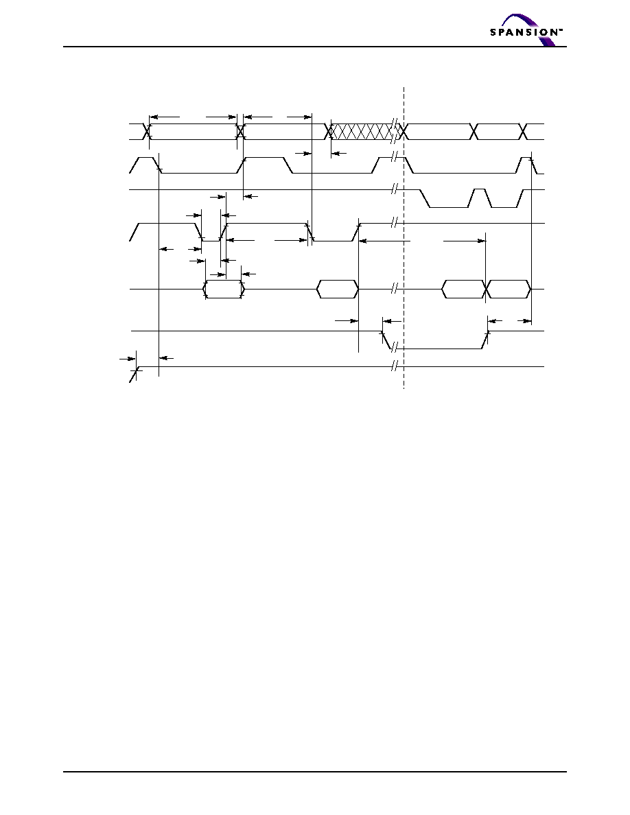
September 8, 2004
S70GL256M00
49
P R E L I M I N A R Y
AC CHARACTERISTICS
OE#
CE#
Addresses
V
CC
WE#
Data
2AAh
SA
t
AH
t
WP
t
WC
t
AS
t
WPH
555h for chip erase
10 for Chip Erase
30h
t
DS
t
VCS
t
CS
t
DH
55h
t
CH
In
Progress
Complete
t
WHWH2
VA
VA
Erase Command Sequence (last two cycles)
Read Status Data
RY/BY#
t
RB
t
BUSY
Notes:
1. SA = sector address (for Sector Erase), VA = Valid Address for reading status data (see "Write Operation Status").
2. These waveforms are for the doubleword mode.
Figure 19.
Chip/Sector Erase Operation Timings
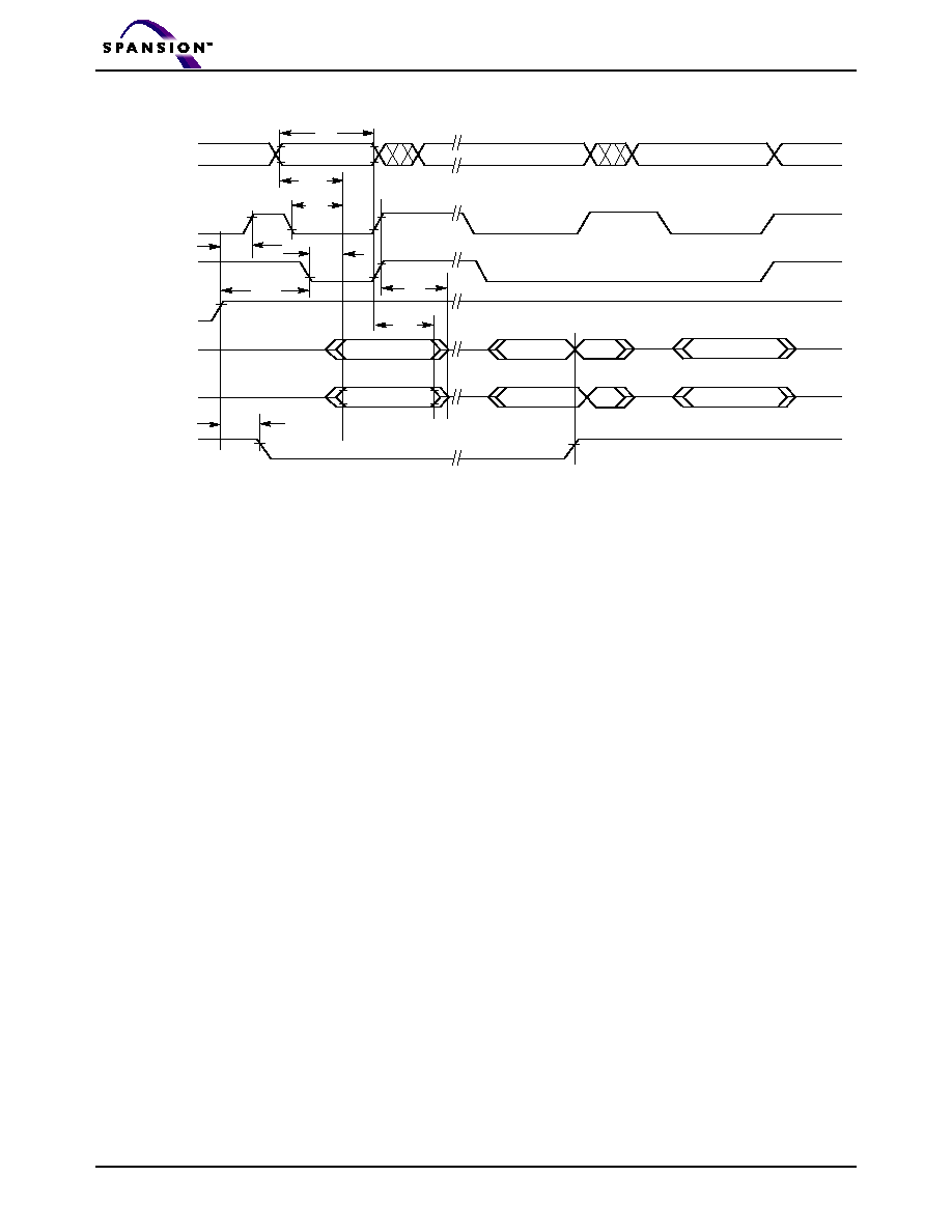
50
S70GL256M00
September 8, 2004
P R E L I M I N A R Y
AC CHARACTERISTICS
WE#
CE#
OE#
High Z
t
OE
High Z
DQ7
DQ0≠DQ6
RY/BY#
t
BUSY
Complement
True
Addresses
VA
t
OEH
t
CE
t
CH
t
OH
t
DF
VA
VA
Status Data
Complement
Status Data
True
Valid Data
Valid Data
t
ACC
t
RC
Note: VA = Valid address. Illustration shows first status cycle after command sequence, last status read cycle, and array data
read cycle.
Figure 20.
Data# Polling Timings (During Embedded Algorithms)
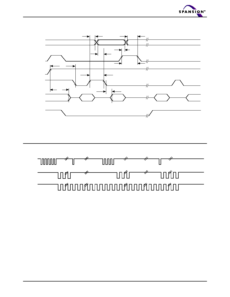
September 8, 2004
S70GL256M00
51
P R E L I M I N A R Y
AC CHARACTERISTICS
OE#
CE#
WE#
Addresses
t
OEH
t
DH
t
AHT
t
ASO
t
OEPH
t
OE
Valid Data
(first read)
(second read)
(stops toggling)
t
CEPH
t
AHT
t
AS
DQ6/DQ2
Valid Data
Valid
Status
Valid
Status
Valid
Status
RY/BY#
Note: VA = Valid address; not required for DQ6 and DQ14. Illustration shows first two status cycle after command sequence,
last status read cycle, and array data read cycle
Figure 21.
Toggle Bit Timings (During Embedded Algorithms)
Note: DQ2 and DQ10 toggle only when read at an address within an erase-suspended sector. The system may use OE# or
CE# to toggle DQ2 and DQ1- and DQ6 and DQ14.
Figure 22.
DQ2 vs. DQ6
Enter
Erase
Erase
Erase
Enter Erase
Suspend Program
Erase Suspend
Read
Erase Suspend
Read
Erase
WE#
DQ2,
Erase
Complete
Erase
Suspend
Suspend
Program
Resume
Embedded
Erasing
DQ6,
DQ14
DQ10
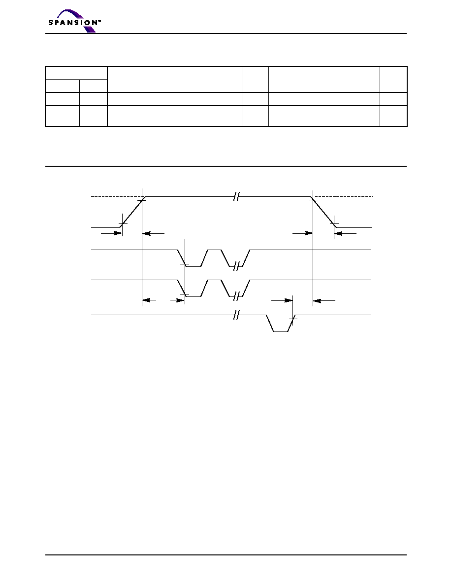
52
S70GL256M00
September 8, 2004
P R E L I M I N A R Y
AC CHARACTERISTICS
Temporary Sector Unprotect
Note:
1. Not 100% tested.
2. AC specifications listed are tested with V
IO
= V
CC
. Contact Spansion for information on AC operation when V
IO
V
CC
Parameter
All Speed Options
JEDEC
Std
Description
Unit
t
VIDR
V
ID
Rise and Fall Time (See Note)
Min
500
ns
t
RSP
RESET# Setup Time for Temporary Sector
Unprotect
Min
4
µs
RESET#
t
VIDR
V
ID
V
SS
, V
IL
,
or V
IH
V
ID
V
SS
, V
IL
,
or V
IH
CE#
WE#
RY/BY#
t
VIDR
t
RSP
Program or Erase Command Sequence
t
RRB
Figure 23.
Temporary Sector Group Unprotect Timing Diagram
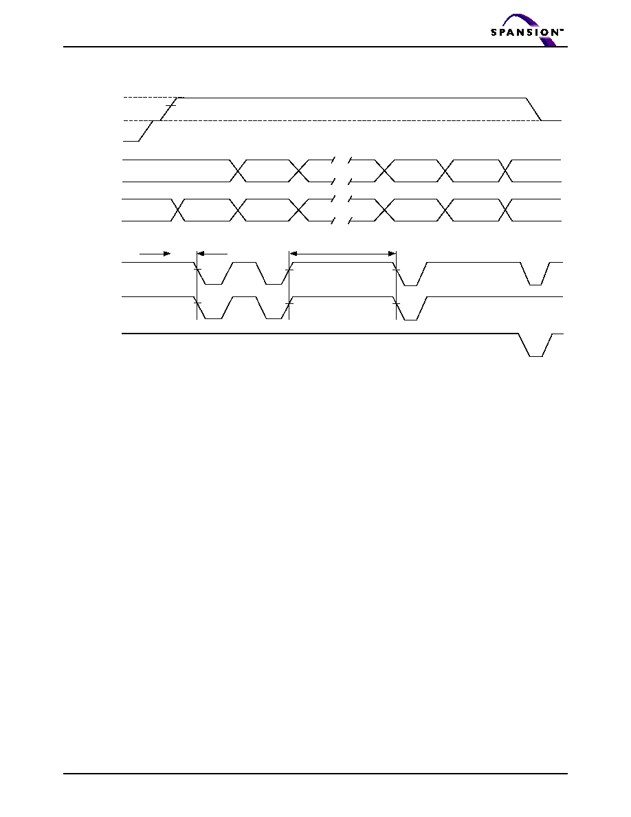
September 8, 2004
S70GL256M00
53
P R E L I M I N A R Y
AC CHARACTERISTICS
Sector Group Protect: 150 µs,
Sector Group Unprotect: 15 ms
1 µs
RESET#
SA, A6,
A1, A0
Data
CE#
WE#
OE#
60h
60h
40h
Valid*
Valid*
Valid*
Status
Sector Group Protect or Unprotect
Verify
V
ID
V
IH
* For sector group protect, A6 = 0, A1 = 1, A0 = 0. For sector group unprotect, A6 = 1, A1 = 1, A0 = 0.
Figure 24.
Sector Group Protect and Unprotect Timing Diagram
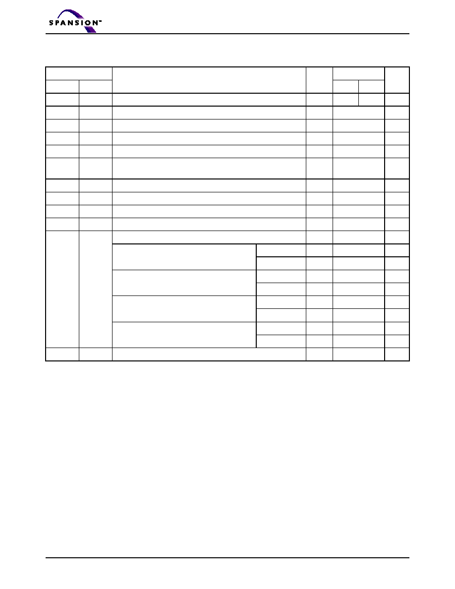
54
S70GL256M00
September 8, 2004
P R E L I M I N A R Y
AC CHARACTERISTICS
Alternate CE# Controlled Erase and Program Operations
Notes:
1. Not 100% tested.
2. See the "Erase And Programming Performance" section for more information.
3. For 1≠16 doublewords/1≠32 words programmed.
4. Effective write buffer specification is based upon a 16-doubleword/32-word write buffer operation.
5. AC specifications listed are tested with V
IO
= V
CC
. Contact Spansion for information on AC operation when V
IO
V
CC
Parameter
Speed Options
JEDEC
Std.
Description
110R
120R
Unit
t
AVAV
t
WC
Write Cycle Time (Note 1)
Min
110
120
ns
t
AVWL
t
AS
Address Setup Time
Min
0
ns
t
ELAX
t
AH
Address Hold Time
Min
45
ns
t
DVEH
t
DS
Data Setup Time
Min
45
ns
t
EHDX
t
DH
Data Hold Time
Min
0
ns
t
GHEL
t
GHEL
Read Recovery Time Before Write
(OE# High to WE# Low)
Min
0
ns
t
WLEL
t
WS
WE# Setup Time
Min
0
ns
t
EHWH
t
WH
WE# Hold Time
Min
0
ns
t
ELEH
t
CP
CE# Pulse Width
Min
45
ns
t
EHEL
t
CPH
CE# Pulse Width High
Min
30
ns
t
WHWH1
t
WHWH1
Write Buffer Program Operation (Notes 2, 3)
Typ
240
µs
Effective Write Buffer Program Operation (Notes
2, 4)
Per Word
Typ
7.5
µs
Per Doubleword
Typ
15
µs
Effective Accelerated Write Buffer Program
Operation (Notes 2, 4)
Per Word
Typ
6.25
µs
Per Doubleword
Typ
12.5
µs
Single Doubleword/Word Program Operation
(Note 2)
Word
Typ
60
µs
Doubleword
Typ
60
µs
Accelerated Single Doubleword/Word
Programming Operation (Note 2)
Word
Typ
54
µs
Doubleword
Typ
54
µs
t
WHWH2
t
WHWH2
Sector Erase Operation (Note 2)
Typ
0.5
sec
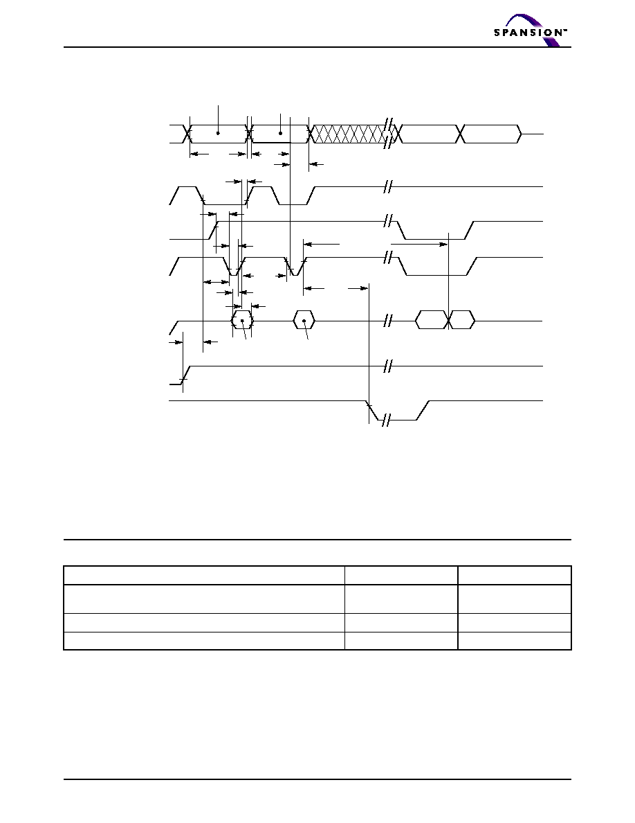
September 8, 2004
S70GL256M00
55
P R E L I M I N A R Y
AC CHARACTERISTICS
LATCHUP CHARACTERISTICS
Note: Includes all pins except V
CC
. Test conditions: V
CC
= 3.0 V, one pin at a time.
Description
Min
Max
Input voltage with respect to V
SS
on all pins except I/O pins
(including A9, OE#, and RESET#)
≠1.0 V
12.5 V
Input voltage with respect to V
SS
on all I/O pins
≠1.0 V
V
CC
+ 1.0 V
V
CC
Current
≠100 mA
+100 mA
t
GHEL
t
WS
OE#
CE#
WE#
RESET#
t
DS
Data
t
AH
Addresses
t
DH
t
CP
DQ7#
D
OUT
t
WC
t
AS
t
CPH
PA
Data# Polling
A0 for program
55 for erase
t
RH
t
WHWH1 or 2
RY/BY#
t
WH
PD for program
30 for sector erase
10 for chip erase
555 for program
2AA for erase
PA for program
SA for sector erase
555 for chip erase
t
BUSY
Notes:
1. Figure indicates last two bus cycles of a program or erase operation.
2. PA = program address, SA = sector address, PD = program data.
3. DQ7# and DQ15# are the complement of the data written to the device. D
OUT
is the data written to the device.
4. Waveforms are for the word mode.
Figure 25.
Alternate CE# Controlled Write (Erase/Program)
Operation Timings
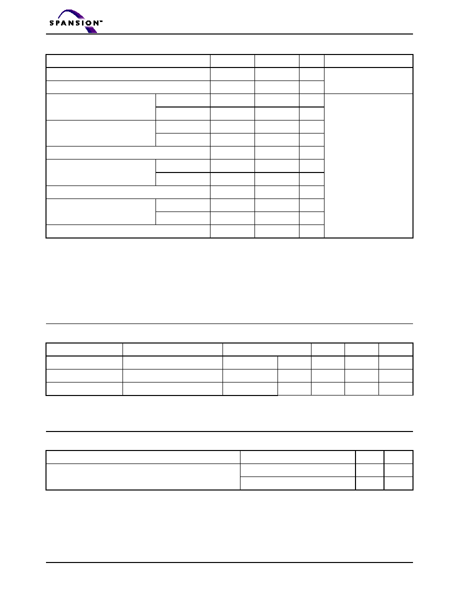
56
S70GL256M00
September 8, 2004
P R E L I M I N A R Y
ERASE AND PROGRAMMING PERFORMANCE
Notes:
1. Typical program and erase times assume the following conditions: 25∞C, 3.0 V V
CC
, 10,000 cycles. Additionally,
programming typicals assume checkerboard pattern.
2. Under worst case conditions of 90∞C, V
CC
= 3.0 V, 100,000 cycles.
3. Effective write buffer specification is based upon a 16-doubleword/32-word write buffer operation.
4. For 1≠16 doublewords or 1-32 words programmed in a single write buffer programming operation.
5. In the pre-programming step of the Embedded Erase algorithm, all bits are programmed to 00h before erasure.
6. System-level overhead is the time required to execute the two- or four-bus-cycle sequence for the program command. See Tables
10 and 11 for further information on command definitions.
TSOP PIN AND BGA PACKAGE CAPACITANCE
Notes:
1. Sampled, not 100% tested.
2. Test conditions T
A
= 25∞C, f = 1.0 MHz.
DATA RETENTION
Parameter
Typ (Note 1)
Max (Note 2)
Unit
Comments
Sector Erase Time
0.5
3.5
sec
Excludes 00h programming
prior to erasure (Note 5)
Chip Erase Time
128
256
sec
Single Doubleword/Word Program
Time (Note 3)
Word
60
600
µs
Excludes system level
overhead (Note 6)
Doubleword
60
600
µs
Accelerated Single Doubleword/
Word Program Time
Word
54
540
µs
Doubleword
54
540
µs
Total Write Buffer Program Time (Note 4)
240
1200
µs
Effective Write Buffer Program
Time (Note 3)
Per Word
7.5
38
µs
Per Doubleword
15
75
µs
Total Accelerated Write Buffer Program Time (Note 4)
200
1040
µs
Effective Write Buffer Accelerated
Program Time (Note 3)
Per Word
6.25
33
µs
Per Doubleword
12.5
65
µs
Chip Program Time
126
292
sec
Parameter Symbol
Parameter Description
Test Setup
Typ
Max
Unit
C
IN
Input Capacitance
V
IN
= 0
BGA
TBD
TBD
pF
C
OUT
Output Capacitance
V
OUT
= 0
BGA
TBD
TBD
pF
C
IN2
Control Pin Capacitance
V
IN
= 0
BGA
TBD
TBD
pF
Parameter Description
Test Conditions
Min
Unit
Minimum Pattern Data Retention Time
150∞C
10
Years
125∞C
20
Years
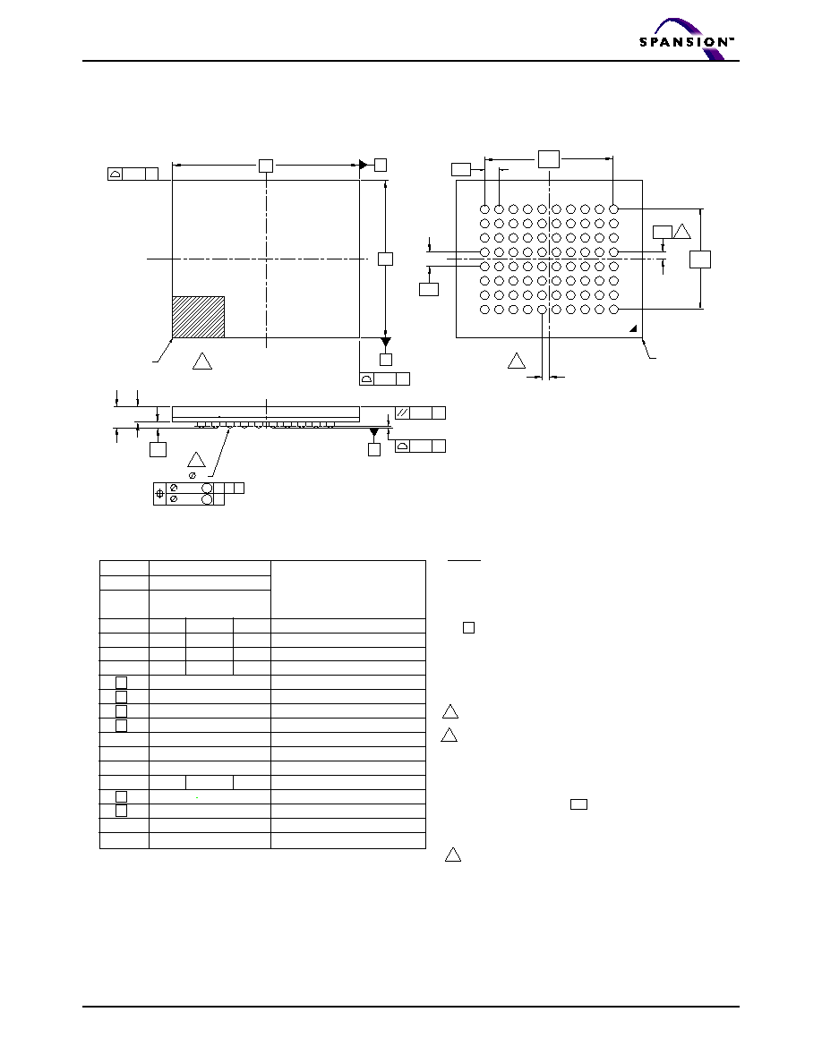
September 8, 2004
S70GL256M00
57
P R E L I M I N A R Y
PHYSICAL DIMENSIONS
LSB080≠80-Ball Fortified Ball Grid Array (Fortified BGA)
13 x 11 mm Package
3265 \ 16-038.15a
PACKAGE
LSB 080
JEDEC
N/A
D x E
13.00 mm x 11.00 mm
PACKAGE
SYMBOL
MIN
NOM
MAX
NOTE
A
---
---
1.60
PROFILE
A1
0.40
---
---
BALL HEIGHT
A2
1.00
---
1.11
BODY THICKNESS
D
13.00 BSC.
BODY SIZE
E
11.00 BSC.
BODY SIZE
D1
9.00 BSC.
MATRIX FOOTPRINT
E1
7.00 BSC.
MATRIX FOOTPRINT
MD
10
MATRIX SIZE D DIRECTION
ME
8
MATRIX SIZE E DIRECTION
n
80
BALL COUNT
b
0.50
0.60
0.70
BALL DIAMETER
eE
1.00 BSC.
BALL PITCH
eD
1.00 BSC
BALL PITCH
SD / SE
0.50 BSC.
SOLDER BALL PLACEMENT
DEPOPULATED SOLDER BALLS
NOTES:
1.
DIMENSIONING AND TOLERANCING METHODS PER
ASME Y14.5M-1994.
2.
ALL DIMENSIONS ARE IN MILLIMETERS.
3.
BALL POSITION DESIGNATION PER JESD 95-1, SPP-010.
4.
e REPRESENTS THE SOLDER BALL GRID PITCH.
5.
SYMBOL "MD" IS THE BALL MATRIX SIZE IN THE "D"
DIRECTION.
SYMBOL "ME" IS THE BALL MATRIX SIZE IN THE
"E" DIRECTION.
n IS THE NUMBER OF POPULTED SOLDER BALL POSITIONS
FOR MATRIX SIZE MD X ME.
6
DIMENSION "b" IS MEASURED AT THE MAXIMUM BALL
DIAMETER IN A PLANE PARALLEL TO DATUM C.
7
SD AND SE ARE MEASURED WITH RESPECT TO DATUMS A
AND B AND DEFINE THE POSITION OF THE CENTER SOLDER
BALL IN THE OUTER ROW.
WHEN THERE IS AN ODD NUMBER OF SOLDER BALLS IN THE
OUTER ROW SD OR SE = 0.000.
WHEN THERE IS AN EVEN NUMBER OF SOLDER BALLS IN THE
OUTER ROW, SD OR SE = e/2
8.
"+" INDICATES THE THEORETICAL CENTER OF DEPOPULATED
BALLS.
9.
N/A
10 A1 CORNER TO BE IDENTIFIED BY CHAMFER, LASER OR INK
MARK, METALLIZED MARK INDENTATION OR OTHER MEANS.
80X
C
0.20
(2X)
(2X)
C
0.20
B
A
6
b
0.25 C
C
0.25 M C
M C
A B
0.10
D
E
C
TOP VIEW
SIDE VIEW
A2
A1
A
0.20
10
INDEX MARK
CORNER
PIN A1
BOTTOM VIEW
K
J
eD
CORNER
E1
7
SE
D1
A
B
D
C
E
F
H
G
8
7
5
6
4
2
3
1
eE
SD
PIN A1
7

58
S70GL256M00
September 8, 2004
P R E L I M I N A R Y
REVISION SUMMARY
Revision A (September 8, 2004)
Initial release.
Colophon
The products described in this document are designed, developed and manufactured as contemplated for general use, including without limita-
tion, ordinary industrial use, general office use, personal use, and household use, but are not designed, developed and manufactured as con-
templated (1) for any use that includes fatal risks or dangers that, unless extremely high safety is secured, could have a serious effect to the
public, and could lead directly to death, personal injury, severe physical damage or other loss (i.e., nuclear reaction control in nuclear facility,
aircraft flight control, air traffic control, mass transport control, medical life support system, missile launch control in weapon system), or (2) for
any use where chance of failure is intolerable (i.e., submersible repeater and artificial satellite). Please note that Spansion will not be liable to
you and/or any third party for any claims or damages arising in connection with above-mentioned uses of the products. Any semiconductor de-
vices have an inherent chance of failure. You must protect against injury, damage or loss from such failures by incorporating safety design mea-
sures into your facility and equipment such as redundancy, fire protection, and prevention of over-current levels and other abnormal operating
conditions. If any products described in this document represent goods or technologies subject to certain restrictions on export under the Foreign
Exchange and Foreign Trade Law of Japan, the US Export Administration Regulations or the applicable laws of any other country, the prior au-
thorization by the respective government entity will be required for export of those products.
Trademarks
Copyright © 2004 Spansion LLC. All rights reserved.
Spansion, the Spansion logo, and combinations thereof are registered trademarks of Spansion LLC.
ExpressFlash is a trademark of Spansion LLC.
Product names used in this publication are for identification purposes only and may be trademarks of their respective companies.