Document Outline
- S71JL128HC0/128HB0/064HB0/ 064HA0/064H80
- S29JL064H
- 16 Mb SRAM (supplier 1)
- 8 Mb pSRAM (supplier 2)
- 16 Mb pSRAM (supplier 2)
- 16 Mb pSRAM (supplier 4)
- 32 Mb pSRAM (Supplier 3)
- 64 Mb pSRAM (supplier 3)
- 8 Mb SRAM (supplier 1)
- Functional Description
- Absolute Maximum Ratings
- DC Characteristics
- AC Characteristics
- Read/Write Charcteristics (VCC=2.7-3.3V)
- Data Retention Characteristics
- Timing Diagrams
- Figure 60. Timing Waveform of Read Cycle(1) (address controlled, CD#1=OE#=VIL, CS2=WE#=VIH, UB# and/or LB#=VIL)
- Figure 61. Timing Waveform of Read Cycle(2) (WE#=VIH, if BYTE# is low, ignore UB#/LB# timing)
- Figure 62. Timing Waveform of Write Cycle(1) (WE# controlled, if BYTE# is low, ignore UB#/LB# timing)
- Figure 63. Timing Waveform of Write Cycle(2) (CE1# controlled, if BYTE# is low, ignore UB#/LB# timing)
- Figure 64. Timing Waveform of Write Cycle(3) (UB#, LB# controlled, BYTE# must be high)
- Data Retention Waveforms
- Revision Summary
Publication Number S29JLxxxHxx_00 Revision A Amendment 2 Issue Date February 26, 2004
PRELIMINARY
DISTINCTIVE CHARACTERISTICS
MCP Features
Operating Voltage Range of 2.7 to 3.3 V
High Performance
-- Access time as fast as 55 ns
Packages
-- 73-ball FBGA--8 x 11.6 mm
-- 88-ball FBGA--8 x 11.6 mm
Operating Temperatures
-- Wireless: ≠25∞C to +85∞C
-- Industrial: ≠40∞C to +85∞C
GENERAL DESCRIPTION
The S71JLxxxH Series is a product line of stacked Multi-Chip
Products (MCP) and consists of
One or more S29JL064H Flash devices
SRAM or pSRAM options
-- 8Mb x 8/x 16 SRAM
-- 16Mb x 16-only SRAM
-- pSRAM x 16 only:
8Mb pSRAM
16Mb pSRAM
32Mb pSRAM
64Mb pSRAM
The products covered by this document are listed below. For
details about their specifications, please refer to the individual
constituent data sheets for further details.
MCP
Number of S29JL064H
Total Flash Density
SRAM/pSRAM Density
S71JL064H80
1
64Mb
8Mb
S71JL064HA0
1
64Mb
16Mb
S71JL064HB0
1
64Mb
32Mb
S71JL128HB0
2
128Mb
32Mb
S71JL128HC0
2
128Mb
64Mb
Notes:
1. This MCP is only guaranteed to operate @ 2.7 - 3.3 V regardless of component operating ranges.
2. BYTE# operation is only supported on the S71JL064H80xx0x.
S71JL128HC0/128HB0/064HB0/
064HA0/064H80
Stacked Multi-Chip Product (MCP) Flash Memory
and pSRAM CMOS 3.0 Volt-only,
Simultaneous Operation Flash Memories and
Static RAM/Pseudo-static RAM
2
S71JL128HC0/128HB0/064HB0/064HA0/064H80
S29JLxxxHxx_00A2 February 26, 2004
P r e l i m i n a r y
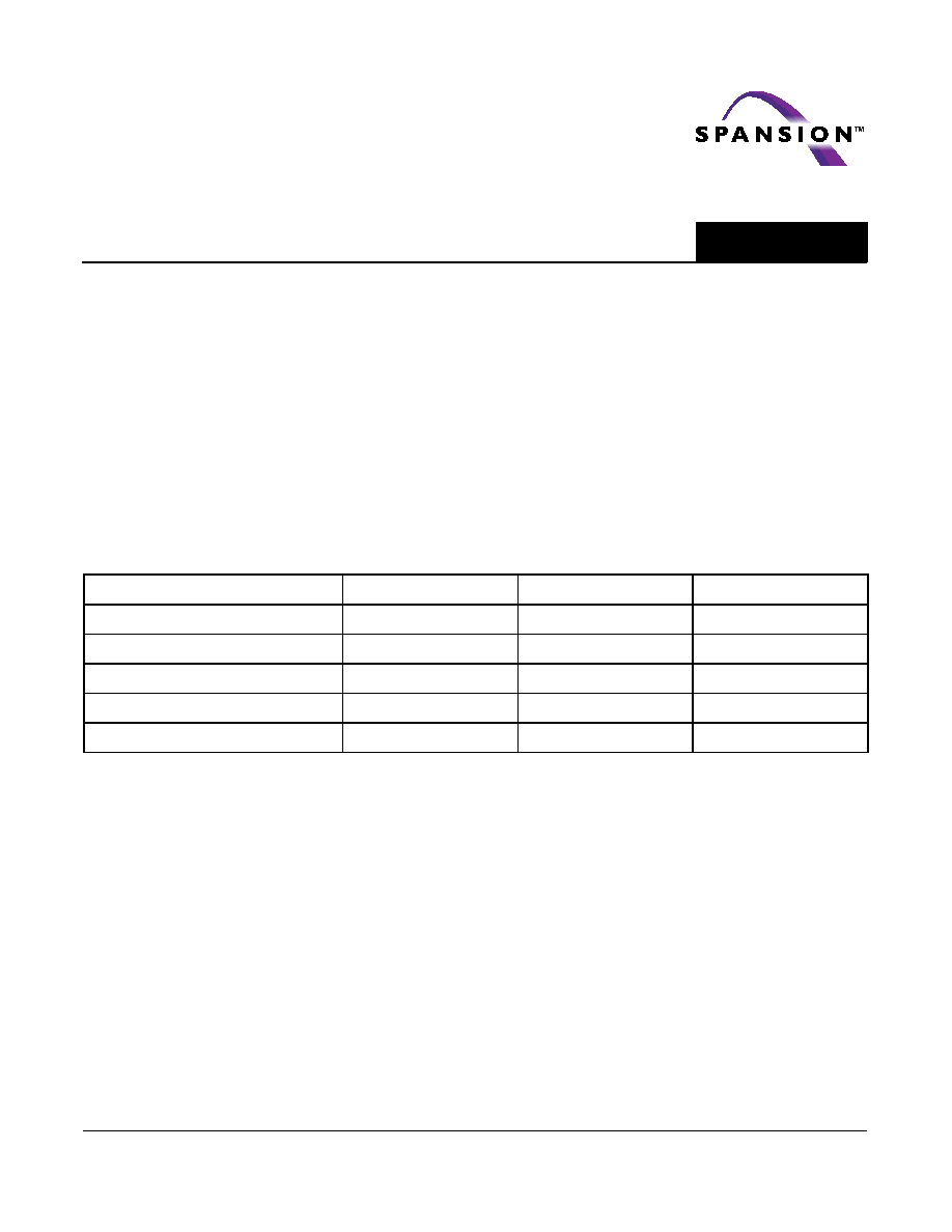
Product Selector Guide
Device-Model #
SRAM/pSRAM Density
SRAM/pSRAM Type
Supplier
Flash Access
Time (ns)
RAM Access
Time (ns)
Packages
S71JL064H80Bxx01
8Mb
SRAM - x8/x16
Supplier 1
70
70
FLB073
S71JL064H80Bxx02
8Mb
SRAM - x8/x16
Supplier 1
85
85
FLB073
S71JL064H80Bxx10
8Mb
pSRAM - x16
Supplier 2
55
55
FLJ073
S71JL064H80Bxx11
8Mb
pSRAM - x16
Supplier 2
70
70
FLJ073
S71JL064H80Bxx12
8Mb
pSRAM - x16
Supplier 2
85
85
FLJ073
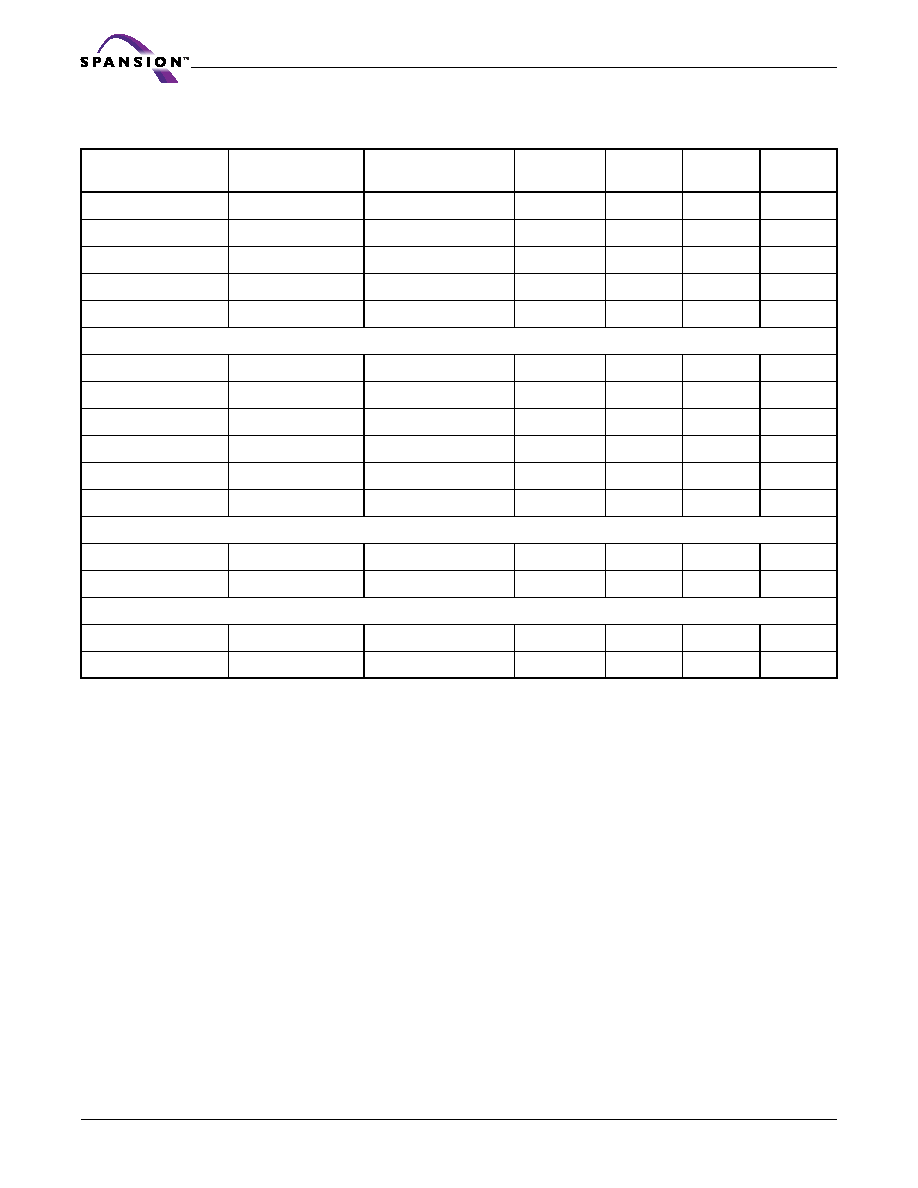
S71JL064HA0Bxx01
16Mb
SRAM - x16
Supplier 1
70
70
FLB073
S71JL064HA0Bxx02
16Mb
SRAM - x16
Supplier 1
85
85
FLB073
S71JL064HA0Bxx10
16Mb
pSRAM - x16
Supplier 2
55
55
FLJ073
S71JL064HA0Bxx11
16Mb
pSRAM - x16
Supplier 2
70
70
FLJ073
S71JL064HA0Bxx12
16Mb
pSRAM - x16
Supplier 2
85
85
FLJ073
S71JL064HA0Bxx62
16Mb
pSRAM - x16
Supplier 4
70
70
FLJ073
S71JL128HB0Bxx01
32Mb
pSRAM - x16
Supplier 3
70
70
FTA073
S71JL128HB0Bxx02
32Mb
pSRAM - x16
Supplier 3
85
85
FTA073
S71JL128HC0Bxx01
64Mb
pSRAM - x16
Supplier 3
70
70
FTA088
S71JL128HC0Bxx02
64Mb
pSRAM - x16
Supplier 3
85
85
FTA088

February 24, 2004 S71JLxxxHxx_00A0
3
A d v a n c e I n f o r m a t i o n
TABLE OF CONTENTS
S71JL128HC0/128HB0/064HB0/064HA0/064H80
Distinctive Characteristics . . . . . . . . . . . . . . . . . . . . 1
General Description . . . . . . . . . . . . . . . . . . . . . . . . . 1
Product Selector Guide . . . . . . . . . . . . . . . . . . . . . .2
Block Diagrams . . . . . . . . . . . . . . . . . . . . . . . . . . . . 6
MCP Block Diagram of S71JL064H80, Model Numbers 01/02 ................6
MCP Block Diagram of S71JL064H80, Model Numbers 10/11/12 ..............6
MCP Block Diagram of S71JL064HA0, Model Numbers 01/02 ................7
MCP Block Diagram of S71JL064HA0, Model Numbers 10/11/12/61 ........7
MCP Block Diagram of S71JL064HB0, Model Numbers 00/01/02 ..........8
MCP Block Diagram of S71JL128HB0, Model Numbers 00/01/02 ...........9
MCP Block Diagram of S71JL128HC0, Model Numbers 00/01/02 ........ 10
Connection Diagrams . . . . . . . . . . . . . . . . . . . . . . 11
Connection Diagram of S71JL064H80, Model Numbers 01/02 .............. 11
Special Package Handling Instructions ...................................................... 12
Pin Description ................................................................................................ 12
Logic Symbol .....................................................................................................13
Connection Diagram of S71JL064H80, Model Numbers 10/11/12 ........... 14
Pin Description .................................................................................................15
Logic Symbol .....................................................................................................15
Connection Diagram of S71JL064HA0, Model Numbers 01/02 ............. 16
Pin Description .................................................................................................17
Logic Symbol .................................................................................................... 18
Connection Diagram of S71JL064HA0, Model Numbers 10/11/12/61 ..... 19
Pin Description ............................................................................................... 20
Logic Symbol ................................................................................................... 20
Connection Diagram of S71JL064HB0, Model Numbers 00/01/02 ....... 21
Pin Description ............................................................................................... 22
Logic Symbol ................................................................................................... 22
Connection Diagram of S71JL128HB0, Model Numbers 00/01/02 ........23
Pin Description ............................................................................................... 24
Logic Symbol ................................................................................................... 24
Connection Diagram of S71JL128HC0, Model Numbers 00/01/02 .......25
Special Package Handling Instructions ......................................................25
Pin Description ............................................................................................... 26
Logic Symbol ................................................................................................... 26
Look-ahead Connection Diagram ..................................................................27
Ordering Information . . . . . . . . . . . . . . . . . . . . . . .29
Physical Dimensions . . . . . . . . . . . . . . . . . . . . . . . 33
FLB073 ....................................................................................................................33
FLJ073 ......................................................................................................................34
FTA073 ...................................................................................................................35
FTA088 ..................................................................................................................36
S29JL064H
General Description 38
Simultaneous Read/Write Operations with Zero Latency ....................38
S71JLxxxHxx_00 Features ................................................................................38
Product Selector Guide . . . . . . . . . . . . . . . . . . . . .40
Block Diagram . . . . . . . . . . . . . . . . . . . . . . . . . . . 40
Pin Description . . . . . . . . . . . . . . . . . . . . . . . . . . . . 41
Logic Symbol . . . . . . . . . . . . . . . . . . . . . . . . . . . . . . 41
Device Bus Operations . . . . . . . . . . . . . . . . . . . . . .42
Table 1. S71JLxxxHxx_00 Device Bus Operations .................. 42
Word/Byte Configuration ................................................................................43
Requirements for Reading Array Data ........................................................ 43
Writing Commands/Command Sequences ................................................ 43
Accelerated Program Operation ...............................................................44
Autoselect Functions .....................................................................................44
Simultaneous Read/Write Operations with Zero Latency ...................44
Standby Mode ......................................................................................................44
Automatic Sleep Mode .....................................................................................44
RESET#: Hardware Reset Pin ......................................................................... 45
Output Disable Mode ....................................................................................... 45
Table 2. S29JL064H Sector Architecture ............................... 46
Table 3. Bank Address ........................................................ 49
Table 4. SecSiTM Sector Addresses ...................................... 49
Autoselect Mode ................................................................................................49
Sector/Sector Block Protection and Unprotection .................................50
Table 5. S71JLxxxHxx_00 Boot Sector/Sector Block Addresses for
Protection/Unprotection ...................................................... 50
Write Protect (WP#) ........................................................................................ 51
Table 6. WP#/ACC Modes ................................................... 52
Temporary Sector Unprotect ........................................................................ 52
Figure 1. Temporary Sector Unprotect Operation ................... 52
Figure 2. In-System Sector Protect/Unprotect Algorithms ....... 53
SecSiTM (Secured Silicon) Sector Flash Memory Region .......................... 53
Factory Locked: SecSi Sector Programmed and Protected At the
Factory ............................................................................................................... 54
Customer Lockable: SecSi Sector NOT Programmed or Protected At
the Factory .......................................................................................................54
Figure 3. SecSi Sector Protect Verify .................................... 55
Hardware Data Protection ............................................................................. 55
Low VCC Write Inhibit ................................................................................ 55
Write Pulse "Glitch" Protection ............................................................... 55
Logical Inhibit ................................................................................................... 56
Power-Up Write Inhibit ............................................................................... 56
Common Flash Memory Interface (CFI) . . . . . . 56
Table 7. CFI Query Identification String ................................ 56
Table 8. System Interface String ......................................... 57
Table 9. Device Geometry Definition .................................... 57
Table 10. Primary Vendor-Specific Extended Query ................ 58
Command Definitions . . . . . . . . . . . . . . . . . . . . . . 59
Reading Array Data ........................................................................................... 59
Reset Command ................................................................................................. 59
Autoselect Command Sequence ....................................................................60
Enter SecSiTM Sector/Exit SecSi Sector Command Sequence ................60
Byte/Word Program Command Sequence .................................................60
Unlock Bypass Command Sequence .........................................................61
Figure 4. Program Operation ............................................... 62
Chip Erase Command Sequence ...................................................................62
Sector Erase Command Sequence ................................................................ 63
Figure 5. Erase Operation ................................................... 64
Erase Suspend/Erase Resume Commands ..................................................64
Table 11. S29JL064H Command Definitions .......................... 65
Write Operation Status . . . . . . . . . . . . . . . . . . . . 66
DQ7: Data# Polling ............................................................................................66
Figure 6. Data# Polling Algorithm ........................................ 68
RY/BY#: Ready/Busy# .......................................................................................68
DQ6: Toggle Bit I ...............................................................................................69
Figure 7. Toggle Bit Algorithm ............................................. 70
DQ2: Toggle Bit II ..............................................................................................70
Reading Toggle Bits DQ6/DQ2 ...................................................................... 71
DQ5: Exceeded Timing Limits ......................................................................... 71

4
S71JLxxxHxx_00A0 February 24, 2004
A d v a n c e I n f o r m a t i o n
DQ3: Sector Erase Timer ..................................................................................71
Table 12. Write Operation Status ......................................... 72
Absolute Maximum Ratings . . . . . . . . . . . . . . . . . . 73
Figure 8. Maximum Negative Overshoot Waveform................. 73
Figure 9. Maximum Positive Overshoot Waveform .................. 73
Operating Ranges . . . . . . . . . . . . . . . . . . . . . . . . . .73
Wireless (W) Devices ...................................................................................73
Industrial (I) Devices ......................................................................................73
V
CC
Supply Voltages ......................................................................................73
DC Characteristics . . . . . . . . . . . . . . . . . . . . . . . . 74
Table 13. CMOS Compatible ................................................ 74
Zero-Power Flash ...............................................................................................75
Figure 10. I
CC1
Current vs. Time (Showing Active and Automatic
Sleep Currents).................................................................. 75
Figure 11. Typical ICC1 vs. Frequency................................... 75
Test Conditions ...................................................................................................76
Figure 12. Test Setup ........................................................ 76
Table 14. Test Specifications ............................................... 76
Switching Waveforms ........................................................................................76
Table 15. Key To Switching Waveforms ................................ 76
Figure 13. Input Waveforms and Measurement Levels............. 76
AC Characteristics . . . . . . . . . . . . . . . . . . . . . . . . 77
Read-Only Operations ......................................................................................77
Figure 14. Read Operation Timings ....................................... 77
Hardware Reset (RESET#) .............................................................................. 78
Figure 15. Reset Timings..................................................... 78
Word/Byte Configuration (BYTE#) ............................................................. 78
Figure 16. BYTE# Timings for Read Operations ...................... 79
Figure 17. BYTE# Timings for Write Operations ...................... 79
Erase and Program Operations .....................................................................80
Figure 18. Program Operation Timings .................................. 81
Figure 19. Accelerated Program Timing Diagram .................... 81
Figure 20. Chip/Sector Erase Operation Timings ..................... 82
Figure 21. Back-to-back Read/Write Cycle Timings ................. 82
Figure 22. Data# Polling Timings (During Embedded Algorithms) .
83
Figure 23. Toggle Bit Timings (During Embedded Algorithms) .. 83
Figure 24. DQ2 vs. DQ6 ...................................................... 84
Temporary Sector Unprotect ........................................................................ 84
Figure 25. Temporary Sector Unprotect Timing Diagram.......... 84
Figure 26. Sector/Sector Block Protect and Unprotect Timing
Diagram............................................................................ 85
Alternate CE# Controlled Erase and Program Operations ................. 86
Figure 27. Alternate CE# Controlled Write (Erase/Program)
Operation Timings .............................................................. 87
Erase And Programming Performance . . . . . . . .88
Latchup Characteristics . . . . . . . . . . . . . . . . . . . . 88
8 Mb SRAM (supplier 1)
Functional Description . . . . . . . . . . . . . . . . . . . . . 89
Table 16. Word Mode ......................................................... 89
Table 17. Byte Mode .......................................................... 89
Absolute Maximum Ratings . . . . . . . . . . . . . . . . . 90
DC Characteristics . . . . . . . . . . . . . . . . . . . . . . . . 90
Recommended DC Operating Conditions ................................................ 90
Capacitance (f=1MHz, T
A
=25
∞C) ...................................................................90
DC and Operating Characteristics ................................................................ 91
AC Characteristics . . . . . . . . . . . . . . . . . . . . . . . . .92
Read/Write Charcteristics (V
CC
=2.7-3.3V) ................................................ 92
Data Retention Characteristics ..................................................................... 92
Timing Diagrams ..................................................................................................93
Figure 28. Timing Waveform of Read Cycle(1) (address controlled,
CD#1=OE#=V
IL
, CS2=WE#=V
IH
, UB# and/or LB#=V
IL
)........ 93
Figure 29. Timing Waveform of Read Cycle(2) (WE#=V
IH
, if BYTE#
is low, ignore UB#/LB# timing) ........................................... 93
Figure 30. Timing Waveform of Write Cycle(1) (WE# controlled, if
BYTE# is low, ignore UB#/LB# timing)................................. 93
Figure 31. Timing Waveform of Write Cycle(2) (CE1# controlled, if
BYTE# is low, ignore UB#/LB# timing)................................. 94
Figure 32. Timing Waveform of Write Cycle(3) (UB#, LB#
controlled, BYTE# must be high) ......................................... 94
Data Retention Waveforms ............................................................................ 95
Figure 33. CE1# Controlled................................................. 95
Figure 34. CS2 Controlled................................................... 95
16 Mb SRAM (supplier 1)
Functional Description . . . . . . . . . . . . . . . . . . . . . 96
Absolute Maximum Ratings . . . . . . . . . . . . . . . . 96
DC Characteristics . . . . . . . . . . . . . . . . . . . . . . . . 97
Recommended DC Operating Conditions (Note 1) ...............................97
Capacitance (f=1MHz, T
A
=25
∞C) ...................................................................97
DC Operating Characteristics ....................................................................... 97
AC Characteristics . . . . . . . . . . . . . . . . . . . . . . . . .98
Read/Write Charcteristics (V
CC
=2.7-3.3V) ................................................98
Data Retention Characteristics .....................................................................98
Timing Diagrams .................................................................................................99
Figure 35. Timing Waveform of Read Cycle(1) (address controlled,
CD#1=OE#=V
IL
, CS2=WE#=V
IH
, UB# and/or LB#=V
IL
)........ 99
Figure 36. Timing Waveform of Read Cycle(2) (WE#=V
IH
) ...... 99
Figure 37. Timing Waveform of Write Cycle(1) (WE# controlled)...
100
Figure 38. Timing Waveform of Write Cycle(2) (CS# controlled) ...
100
Figure 39. Timing Waveform of Write Cycle(3) (UB#, LB#
controlled)...................................................................... 101
Figure 40. Data Retention Waveform.................................. 102
8 Mb pSRAM (supplier 2)
Features . . . . . . . . . . . . . . . . . . . . . . . . . . . . . . . . 103
General Description . . . . . . . . . . . . . . . . . . . . . . . 103
Block Diagram . . . . . . . . . . . . . . . . . . . . . . . . . . 104
Figure 41. Functional Block Diagram .................................. 104
Table 18. Functional Description ........................................ 104
Absolute Maximum Ratings (See Note) . . . . . . 104
DC Characteristics . . . . . . . . . . . . . . . . . . . . . . . 105
Operating Characteristics (Over Specified Temperature Range) ......105
AC Characteristics . . . . . . . . . . . . . . . . . . . . . . . 105
Table 19. Timing Test Conditions ....................................... 105
Table 20. Timings ............................................................ 106
Timing Diagrams ................................................................................................107
Figure 42. Timing of Read Cycle (CE1# = OE# = V
IL
, WE# = CE2
= V
IH
)............................................................................ 107
Figure 43. Timing Waveform of Read Cycle (WE# = V
IH
) ...... 107
Figure 44. Timing Waveform of Write Cycle (WE# Control) ... 108
Figure 45. Timing Waveform of Write Cycle (CE1# Control)... 108
16 Mb pSRAM (supplier 2)
Features . . . . . . . . . . . . . . . . . . . . . . . . . . . . . . . 109
General Description . . . . . . . . . . . . . . . . . . . . . . 109
Block Diagram . . . . . . . . . . . . . . . . . . . . . . . . . . . 110
Figure 46. Functional Block Diagram .................................. 110

February 24, 2004 S71JLxxxHxx_00A0
5
A d v a n c e I n f o r m a t i o n
Table 21. Functional Description .........................................110
Absolute Maximum Ratings (See Note) . . . . . . . 111
DC Characteristics . . . . . . . . . . . . . . . . . . . . . . . . 111
Operating Characteristics (Over Specified Temperature Range) .......111
AC Characteristics . . . . . . . . . . . . . . . . . . . . . . . . 112
Timing Test Conditions ....................................................................................112
Timings .................................................................................................................. 112
Timings .................................................................................................................. 113
Figure 47. Timing of Read Cycle (CE1# = OE# = V
IL
, WE# = CE2
= V
IH
) ............................................................................ 113
Figure 48. Timing Waveform of Read Cycle (WE# = V
IH
)....... 113
Figure 49. Timing Waveform of Write Cycle (WE# Control) .... 114
Figure 50. Timing Waveform of Write Cycle (CE1# Control, CE2 =
High).............................................................................. 114
16 Mb pSRAM (supplier 4)
Features . . . . . . . . . . . . . . . . . . . . . . . . . . . . . . . . . 115
Description . . . . . . . . . . . . . . . . . . . . . . . . . . . . . . 115
Pin Description . . . . . . . . . . . . . . . . . . . . . . . . . . . 115
Operation Mode . . . . . . . . . . . . . . . . . . . . . . . . . . 116
Absolute Maxumum Ratings (see Note) . . . . . . 116
DC Characteristics . . . . . . . . . . . . . . . . . . . . . . . . 116
Table 22. DC Recommended Operating Conditions ................116
Table 23. DC Characteristics (T
A
= -25∞C to 85∞C, VDD = 2.6 to
3.3V) ..............................................................................117
AC Characteristics . . . . . . . . . . . . . . . . . . . . . . . . 117
Table 24. AC Characteristics and Operating Conditions (T
A
= -25∞C
to 85∞C, V
DD
= 2.6 to 3.3V) ...............................................117
Table 25. AC Test Conditions .............................................118
Figure 51. AC Test Loads................................................... 118
Figure 52. State Diagram .................................................. 119
Table 26. Standby Mode Characteristics ..............................119
Timing Diagrams . . . . . . . . . . . . . . . . . . . . . . . . . 119
Figure 53. Read Cycle 1--Addressed Controlled .................... 119
Figure 54. Read Cycle 2--CS1# Controlled .......................... 120
Figure 55. Write Cycle 1--WE# Controlled ........................... 120
Figure 56. Write Cycle 2--CS1# Controlled .......................... 121
Figure 57. Write Cycle3--UB#, LB# Controlled ..................... 121
Figure 58. Deep Power-down Mode..................................... 122
Figure 59. Power-up Mode................................................. 122
Figure 60. Abnormal Timing............................................... 122
32 Mb pSRAM (Supplier 3)
Features . . . . . . . . . . . . . . . . . . . . . . . . . . . . . . . . 123
Description . . . . . . . . . . . . . . . . . . . . . . . . . . . . . 123
Pin Description . . . . . . . . . . . . . . . . . . . . . . . . . . 123
Operation Mode . . . . . . . . . . . . . . . . . . . . . . . . . 124
Absolute Maxumum Ratings . . . . . . . . . . . . . . . . 124
DC Characteristics . . . . . . . . . . . . . . . . . . . . . . . . 124
Table 27. DC Recommended Operating Conditions (T
A
= -40∞C to
85∞C) ............................................................................. 124
Table 28. DC Characteristics (T
A
= -40∞C to 85∞C, VDD = 2.6 to
3.3V) ............................................................................. 125
Table 29. Capacitance (T
A
= 25∞C, f = 1 MHz) ..................... 125
AC Characteristics . . . . . . . . . . . . . . . . . . . . . . . . 125
Table 30. AC Characteristics and Operating Conditions (T
A
= -40∞C
to 85∞C, V
DD
= 2.6 to 3.3V) .............................................. 125
Table 31. AC Test Conditions ............................................. 126
Timing Diagrams . . . . . . . . . . . . . . . . . . . . . . . . . 127
Figure 61. Read Cycle ...................................................... 127
Figure 62. Page Read Cycle (8 words access) ...................... 128
Figure 63. Write Cycle 1 (WE# controlled) .......................... 129
Figure 64. Write Cycle 2 (CE# controlled) ........................... 130
Figure 65. Deep Power-down Timing .................................. 130
Figure 66. Power-on Timing .............................................. 130
Figure 67. Read Address Skew Provisions ........................... 131
Figure 68. Write Address Skew Provisions........................... 131
64 Mb pSRAM (supplier 3)
Features . . . . . . . . . . . . . . . . . . . . . . . . . . . . . . . . 132
Description . . . . . . . . . . . . . . . . . . . . . . . . . . . . . . 132
Pin Description . . . . . . . . . . . . . . . . . . . . . . . . . . . 132
Operation Mode . . . . . . . . . . . . . . . . . . . . . . . . . . 133
Absolute Maxumum Ratings . . . . . . . . . . . . . . . . 133
DC Characteristics . . . . . . . . . . . . . . . . . . . . . . . . 133
Table 32. DC Recommended Operating Conditions (T
A
= -25∞C to
85∞C) ............................................................................. 133
Table 33. DC Characteristics (T
A
= -25∞C to 85∞C, VDD = 2.6 to
3.3V) ............................................................................. 134
Table 34. Capacitance (T
A
= 25∞C, f = 1 MHz) ..................... 134
AC Characteristics . . . . . . . . . . . . . . . . . . . . . . . . 134
Table 35. AC Characteristics and Operating Conditions (T
A
= -25∞C
to 85∞C, V
DD
= 2.6 to 3.3V) .............................................. 134
Table 36. AC Test Conditions ............................................. 135
Timing Diagrams . . . . . . . . . . . . . . . . . . . . . . . . . 136
Figure 69. Read Cycle ...................................................... 136
Figure 70. Page Read Cycle (8 words access) ...................... 137
Figure 71. Write Cycle 1 (WE# controlled) .......................... 138
Figure 72. Write Cycle 2 (CE# controlled) ........................... 139
Figure 73. Deep Power-down Timing .................................. 139
Figure 74. Power-on Timing .............................................. 139
Figure 75. Read Address Skew Provisions ........................... 140
Figure 76. Write Address Skew Provisions........................... 140
Revision Summary