
Publication Number S71PL127/129JB0_00 Revision A Amendment 0 Issue Date April 15, 2004
ADVANCE
Distinctive Characteristics
MCP Features
Power supply voltage of 2.7 to 3.1 volt
High performance
-- 70 ns maximum access time (Flash)
-- 30 ns maximum page access time (Flash)
-- 70 ns maximum access time (PSRAM)
-- 30 ns maximum page access time (PSRAM)
Package
-- 64-Ball FBGA
Operating Temperature
-- �25�C to +85�C
Flash Memory Features
ARCHITECTURAL ADVANTAGES
128 Mbit Page Mode device
-- Page size of 8 words: Fast page read access from
random locations within the page
Single power supply operation
-- Full Voltage range: 2.7 to 3.1 volt read, erase, and
program operations for battery-powered applications
Dual Chip Enable inputs (PL129J)
-- Two CE# inputs control selection of each half of the
memory space
Simultaneous Read/Write Operation
-- Data can be continuously read from one bank while
executing erase/program functions in another bank
-- Zero latency switching from write to read operations
FlexBank Architecture
-- 4 separate banks, with up to two simultaneous
operations per device
-- Bank A:
16Mbit (4Kw x 8 and 32Kw x 31)
-- Bank B:
48Mbit ( 32Kw x 96)
-- Bank C:
48 Mbit (32Kw x 96)
-- Bank D:
16Mbit (4Kw x 8 and 32Kw x 31)
SecSi
TM
(Secured Silicon) Sector region
-- Up to 128 words accessible through a command
sequence
-- Up to 64 factory-locked words
-- Up to 64 customer-lockable words
Both top and bottom boot blocks in one device
Manufactured on 0.11 �m process technology
Data retention: 20 years typical
Cycling Endurance: 1 million cycles per sector
typical
SOFTWARE FEATURES
Software command-set compatible with JEDEC
42.4 standard
-- Backward compatible with Am29F and Am29LV
families
CFI (Common Flash Interface) compliant
-- Provides device-specific information to the system,
allowing host software to easily reconfigure for
different Flash devices
Erase Suspend / Erase Resume
-- Suspends an erase operation to allow read or program
operations in other sectors of same bank
Unlock Bypass Program command
-- Reduces overall programming time when issuing
multiple program command sequences
HARDWARE FEATURES
Ready/Busy# pin (RY/BY#)
-- Provides a hardware method of detecting program or
erase cycle completion
Hardware reset pin (RESET#)
-- Hardware method to reset the device to reading array
data
WP#/ ACC (Write Protect/Acceleration) input
-- At V
IL
, hardware level protection for the first and last
two 4K word sectors.
-- At V
HH
, provides accelerated programming in a
factory setting
Persistent Sector Protection
-- A command sector protection method to lock
combinations of individual sectors and sector groups
S71PL127/129JB0
Stacked Multi-Chip Package (MCP) Flash Memory and
pSRAM
128 Megabit (8M x 16-Bit) CMOS 3.0 Volt-only
Simultaneous Operation Flash Memory and 32 Megabit
(2M x 16-Bit) CMOS Pseudo Static RAM with Page Mode
2
S71PL127/129JB0
S71PL127/129JB0_00A0 April 15, 2004
P r e l i m i n a r y
to prevent program or erase operations within that
sector
-- Sectors can be locked and unlocked in-system at V
CC
level
Password Sector Protection
-- A sophisticated sector protection method to lock
combinations of individual sectors and sector groups
to prevent program or erase operations within that
sector using a user-defined 64-bit password
PSRAM Features
Power dissipation
-- Operating: 40 mA maximum
-- Standby: 135 �A maximum
CE1#r and CE2r Chip Select
Power down features using CE1#r and CE2r
Data retention supply voltage: 1.5 to 3.1 volt
Byte data control: LB# (DQ0�DQ7), UB#(DQ8�
DQ15)
Product Selector Guide
Note:Both VCCf and VCCr must be the same level when
either part is being accessed.
Part Number
S71PL127JB0BAW9Z#
S71PL127JB0BAW9U#
S71PL127JB0BAW9P#
S71PL127JB0BFW9Z#
S71PL127JB0BFW9U#
S71PL127JB0BFW9P#
S71PL129JB0BAW9Z#
S71PL129JB0BAW9U#
S71PL129JB0BAW9P#
S71PL129JB0BFW9Z#
S71PL129JB0BFW9U#
S71PL129JB0BFW9P#
Supply Voltage
V
CC
= 2.7�3.1 V
V
CC
= 2.7�3.1 V
Supply Voltage
Flash
PSRAM
Max Access Time, ns
70
70
Max CE# Access, ns
70
70
Max Page Access, ns
30
30
Max OE# Access, ns
30
40

April 15, 2004 S71PL127/129JB0_00A0
3
A d v a n c e I n f o r m a t i o n
S71PL127/129JB0
Distinctive Characteristics . . . . . . . . . . . . . . . . . . . 1
MCP Features ........................................................................................................ 1
Flash Memory Features ...................................................................................... 1
PSRAM Features ....................................................................................................2
Product Selector Guide . . . . . . . . . . . 2
Connection Diagram (S71PL127JB0) . . . . . . . . . . . .5
Special Handling Instructions For FBGA Package ...................................5
Input/Output Descriptions (S71PL127JB0) . . . . 6
Absolute Maximum Ratings . . . . . . . . . 10
Figure 1. Maximum Negative Overshoot Waveform................. 10
Figure 2. Maximum Positive
Overshoot Waveform.......................................................... 10
Operating Ranges . . . . . . . . . . . . . 10
BGA Pin Capacitance .......................................................................................... 11
TLA064--64-ball Fine-Pitch Ball Grid Array (FBGA)
8 x 11.6 mm Package ........................................................................................... 12
32Mb pSRAM (Supplier 1)
pSRAM Block Diagram . . . . . . . . . . . . . . . . . . . . 14
Function Truth Table . . . . . . . . . . . . . . . . . . . . . . 15
Power Down . . . . . . . . . . . . . . . . . . . . . . . . . . . . . 15
Power Down .....................................................................................................15
Power Down Program Sequence ...............................................................15
Address Key ..................................................................................................... 16
Recommended Operating Conditions . . . . . . . . 16
pSRAM DC Characteristics . . . . . . . . . . . . . . . . . 17
pSRAM AC Characteristics . . . . . . . . . . . . . . . . . 17
Read Operation ....................................................................................................17
PSRAM AC Characteristics . . . . . . . . . . . . . . . . . 19
Write Operation ................................................................................................. 19
AC Characteristics . . . . . . . . . . . . . . . . . . . . . . . . 20
Power Down Parameters ................................................................................ 20
Other Timing Parameters ............................................................................... 20
AC Characteristics . . . . . . . . . . . . . . . . . . . . . . . . 20
AC Test Conditions .......................................................................................... 20
Figure 3. AC Measurement Output Load Circuit...................... 20
Timing Diagrams . . . . . . . . . . . . . . . . . . . . . . . . . . 21
Figure 4. Read TIming #1 (Basic Timing).............................. 21
Figure 5. Read Timing #2 (OE# and Address Access) ............. 22
Timing Diagrams . . . . . . . . . . . . . . . . . . . . . . . . . 23
Figure 6. Read Timing #3 (LB#/UB# Byte Access) ................. 23
Figure 7. Read Timing #4 (Page Access after CE1# Control Access)
24
Timing Diagrams . . . . . . . . . . . . . . . . . . . . . . . . . 25
Figure 8. Read Timing #5 (Random and Page Address Access) 25
Timing Diagrams . . . . . . . . . . . . . . . . . . . . . . . . . 26
Figure 9. Write Timing #1 (Basic Timing).............................. 26
Figure 10. Write Timing #2 (WE# Control)............................ 27
Timing Diagrams . . . . . . . . . . . . . . . . . . . . . . . . . 28
Figure 11. Write Timing #3-1 (WE#/LB#/UB# Byte Write Control)
28
Figure 12. Write Timing #3-2 (WE#/LB#/UB# Byte Write Control)
29
Timing Diagrams . . . . . . . . . . . . . . . . . . . . . . . . . 30
Figure 13. Write Timing #3-3 (WE#/LB#/UB# Byte Write Control)
30
Figure 14. Write Timing #3-4 (WE#/LB#/UB# Byte Write Control)
31
Timing Diagrams . . . . . . . . . . . . . . . . . . . . . . . . . 32
Figure 15. Read/Write Timing #1-1 (CE1# Control) ............... 32
Figure 16. Read/Write Timing #1-2 (CE1#/WE#/OE# Control) 33
Timing Diagrams . . . . . . . . . . . . . . . . . . . . . . . . . 34
Figure 17. Read/Write Timing #2 (OE#, WE# Control) ........... 34
Figure 18. Read/Write Timing #3 (OE#, WE#, LB#, UB# Control)
35
Timing Diagrams . . . . . . . . . . . . . . . . . . . . . . . . . 35
Figure 19. Power-up Timing #1 ........................................... 35
Figure 20. Power-up Timing #2 ........................................... 36
Timing Diagrams . . . . . . . . . . . . . . . . . . . . . . . . . 36
Figure 21. Power-down Entry and Exit Timing........................ 36
Figure 22. Standby Entry Timing after Read or Write.............. 36
Timing Diagrams . . . . . . . . . . . . . . . . . . . . . . . . . 37
Revision Summary
5
S71PL127/129JB0_00A0 April 15, 2004
A d v a n c e I n f o r m a t i o n
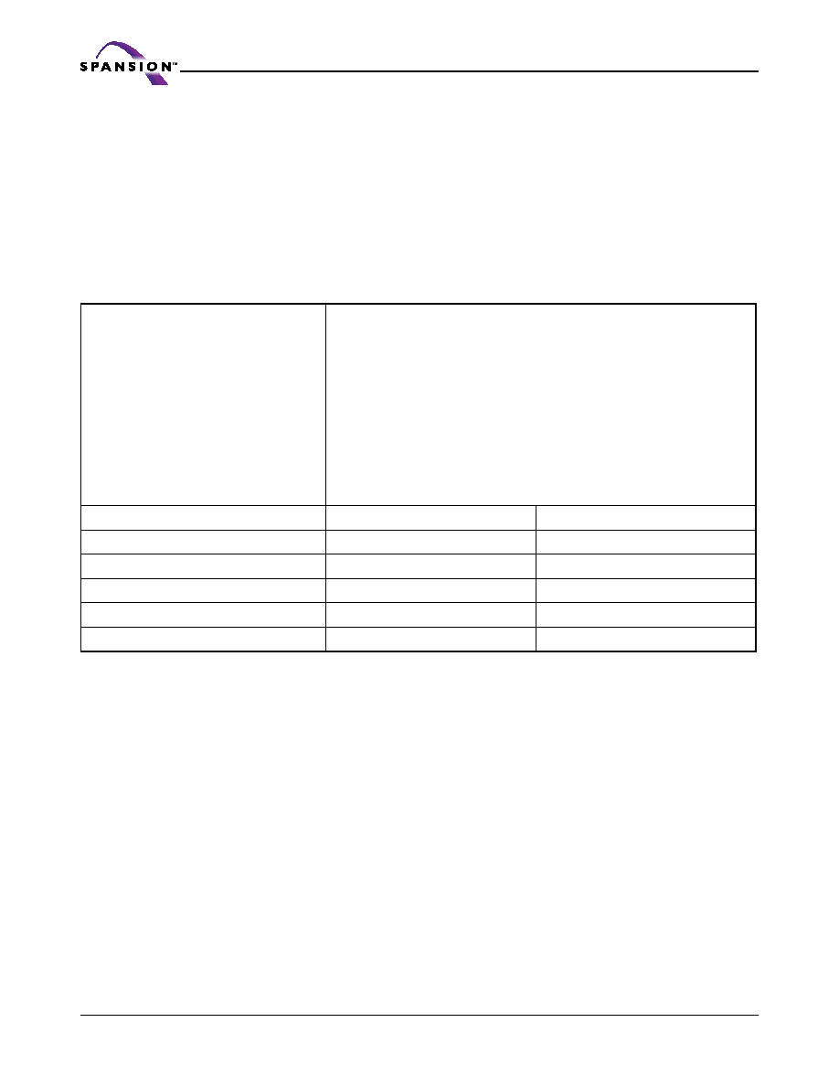
Connection Diagram
(S71PL127JB0)
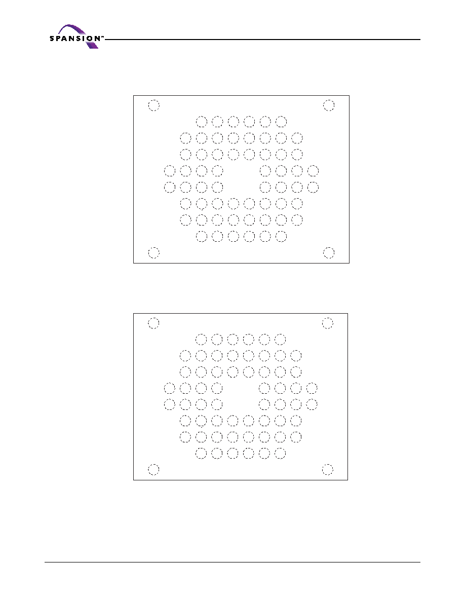
Connection Diagram (S71PL129JB0)
Special Handling Instructions For FBGA Package
Special handling is required for Flash Memory products in FBGA packages.
Flash memory devices in FBGA packages may be damaged if exposed to ultra-
sonic cleaning methods. The package and/or data integrity may be compromised
if the package body is exposed to temperatures above 150�C for prolonged peri-
ods of time.
E7
A13
E6
A9
E5
A20
E4
RY/BY#
E3
A18
E2
A5
A2
E8
A21
G7
N.C.
DQ6
G3
DQ1
G2
VSS
A0
G8
A16
H7
DQ15
H6
DQ13
H5
DQ4
H4
DQ3
H3
DQ9
H2
OE#
CE#f
H8
N. C.
F7
A14
A10
F3
A17
F2
A4
A1
F8
A22
J7
DQ7
J6
DQ12
J5
VCCr
J4
VCCf
J3
DQ10
J2
DQ0
CE1#r
J8
VSS
K7
DQ14
K6
DQ5
K5
N.C.
K4
DQ11
K3
DQ2
DQ8
D7
A12
D6
A19
D5
CE2r
D4
RESET#
D3
UB#
D2
A6
A7
A3
D8
A15
C7
A11
C6
A8
C5
WE#
C4
WP#/ACC
C3
LB#
G4
F4
C8
N.C.
N.C.
K8
E9
G9
H9
F9
J9
D9
N.C.
N.C.
B6
B5
A10
M1
N.C.
M10
N.C.
N.C.
N.C.
A1
L6
L5
64-ball Fine-Pitch Ball Grid Array
(Top View, Balls Facing Down)
E7
A13
E6
A9
E5
A20
E4
RY/BY#
E3
A18
E2
A5
A2
E8
A21
G7
N.C.
DQ6
G3
DQ1
G2
VSS
A0
G8
A16
H7
DQ15
H6
DQ13
H5
DQ4
H4
DQ3
H3
DQ9
H2
OE#
CE0#f
H8
N. C.
F7
A14
A10
F3
A17
F2
A4
A1
F8
CE1#f
J7
DQ7
J6
DQ12
J5
VCCr
J4
VCCf
J3
DQ10
J2
DQ0
CE1#r
J8
VSS
K7
DQ14
K6
DQ5
K5
N.C.
K4
DQ11
K3
DQ2
DQ8
D7
A12
D6
A19
D5
CE2r
D4
RESET#
D3
UB#
D2
A6
A7
A3
D8
A15
C7
A11
C6
A8
C5
WE#
C4
WP#/ACC
C3
LB#
G4
F4
C8
N.C.
N.C.
K8
E9
G9
H9
F9
J9
D9
N.C.
N.C.
B6
B5
A10
M1
N.C.
M10
N.C.
N.C.
N.C.
A1
L6
L5
64-ball Fine-Pitch Ball Grid Array
(Top View, Balls Facing Down)
