
AME, Inc.
1
AME5136
Integrated White LED Driver With
Organic LED Display Power Supply
The AME5136 is a dual Boost DC/DC converter, de-
signed to drive up to 4 white LEDs with a constant cur-
rent and to power an organic LED display with a constant
voltage. According to SEL pin status, the AME5136 can
either regulates output current flowing through series con-
nected LEDs or regulate output voltage applying to OLED.
A single external resistor is used to set the maximum
LED current. The LED current can be adjusted by apply-
ing a PWM signal to the EN pin. Pulling the EN pin to
GND disables the chip and reduces the supply current to
less than 1uA. Additional features include a low-side NFET
switch that can turn off the LED string with no DC current
path to ground. Other features include OVP, OCP, UVP
and OTP.
The AME5136 is available in a small DFN-10(
3mmx3mmx0.85mm) package.
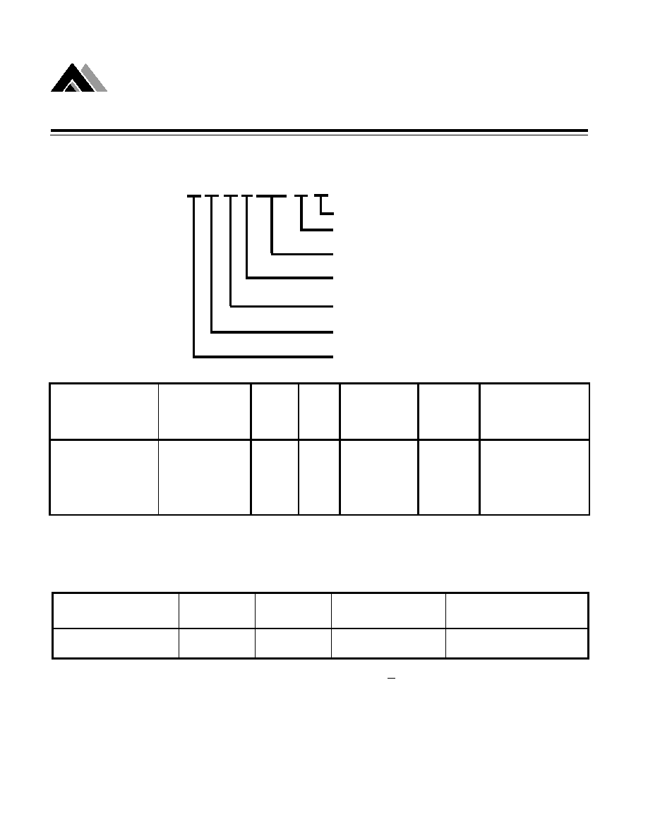
n
General Description
n
Features
n
Applications
l
Integrated OLED and White-LED Driver
l
Wide Input Voltage Range: 2.7V to 5.5V
l
Adjustable output voltage up to 20V
l
Complete Protection: OVP, OTP, UVP
l
PWM Dimming Control
l
Small External Components
l
Cycle-By-Cycle Current Limit
l
All AME's Lead Free Products Meet RoHS
Standards
l
White LED Back-Lighting
l
Hand-held Devices
l
Digital Cameras
l
Flip-phones / Clam-shell Cellular Phones
l
High-fashion cellular phones
Figure 2. 4 LEDs for Main Panel and 3 LEDs for SUB
Panel
Figure 1. Main LEDs Display and OLED SUB Display
n
Typical Application
23
.
1
1
2
1
�
+
=
SUB
SUB
SUB
R
R
V
FB1
SW
GND
L
D
V
IN
AME5136
OVP
R
SUB1
R
SUB2
FB2
CH2
SEL
CH1
10
�
H
Main Display
OLED
SUB
Display
0V
>1.5V
V
IN
2.7V~4.2V
C
IN
4.7
�
F
EN
C
OUT1
1
�
F
V
FB1
R
FB1
ILED1=
0.21
R
FB1
ILED1
V
SUB
Main
47P
FB1
SW
GND
L
D
V
IN
AME5136
OVP
FB2
CH2
SEL
CH1
10
�
H
Main Display
C
OUT2
1
�
F
V
SUB
R
FB2
0V
>1.5V
R
FB1
C
OUT1
1
�
F
C
IN
4.7
�
F
V
IN
2.7V~4.2V
EN
V
FB1
V
FB2
ILED2
ILED1=
0.21
R
FB1
ILED1
ILED2=
1.23
R
FB2
V
SUB
Main

AME, Inc.
2
Integrated White LED Driver With
Organic LED Display Power Supply
AME5136
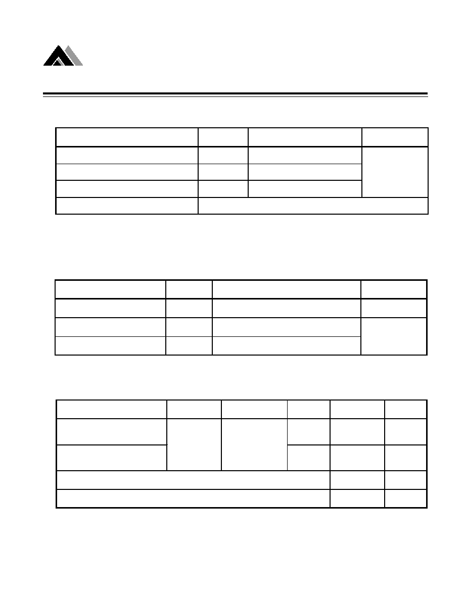
n
Function Block Diagram
Figure 3. AME5136 Function Block Diagram
L
Main Display
R
FB1
FB1
GND
Enable
Current
sensing
SW
CL
COMP
-
UVP
COMP
Logic
N1
CH1
N2
ref1
ref2
Driver
Driver
CH2
FB2
OVP
COMP
OVP
REF
V
IN
C
IN
CP
7
6
400ns
one shut
CL
Adjust
1
V
IN
Select Logic
EN
2
SEL
3
Organic
LED
C1
OVP 9
D
P1
XEnable
Vref
UVP
REF
OTP
5
4
8
10

AME, Inc.
3
AME5136
Integrated White LED Driver With
Organic LED Display Power Supply
Pin Number
Pin Name
Pin Description
1
V
IN
Input Voltage.
2
EN
Shutdown control input, active low.
The shutdown pin is an active low control. Tie this pin above 1.5V to enable
the device. Tie this pin below 0.4V to turn off the device.
3
SEL
Selection Pin. Internal MOSFET selection. Pull low to turn on the internal
CH1. Pull high to turn on CH2.
4
FB1
Main Display Feedback.
5
CH1
Main Display Return Voltage
6
GND
Ground.
7
FB2
SUB Display Feedback.
8
CH2
SUB Display Power Supply Voltage.
9
OVP
Over Voltage Protection.
10
SW
This is the switch pin and is connected to the drain of the internal NMOS
power switch N1.
23
.
1
1
2
1
�
+
=
SUB
SUB
SUB
R
R
V
AME5136AEVB
1. V
IN
2. EN
3. SEL
4. FB1
5. CH1
6. GND
7. FB2
8. CH2
9. OVP
10. SW
* Die Attach:
Conductive Epoxy
DFN-10
(3mmx3mmx0.85mm)
Top View
n
Pin Configuration
n
Pin Description
Note : The area enclosed by dashed line represents Exposed Pad and connect to GND.
9
8
7
1
2
3
4
AME5136
5
6
10
AME, Inc.
4
Integrated White LED Driver With
Organic LED Display Power Supply
AME5136
Operating Ambient Temperature Range
Number of Pins
Package Type
Pin Configuration
Special Feature1
AME5136 x x x
x
xxx
x- x
Output Voltage
n
Ordering Information
Special Feature2
n
Ordering Information
Note: ww represents the date code and pls refer to Date Code Rule page on Package Dimension.
* A line on top of the first letter represents lead free plating such as BDZ.
Please consult AME sales office or authorized Rep./Distributor for the availability of package type.
Part Number
Marking*
Output
Voltage
Package
Operating Ambient
Temperature Range
AME5136AEVBADJZ-3
BDZ
yyww
ADJ
DFN-10
(3mmx3mmx0.85mm)
-40
o
C to +85
o
C
A
1. V
IN
6. GND
E: -40
O
C to +85
O
C V: DFN
B: 10
ADJ: Adjustable Z: Lead free
3: 3x3x0.85(mm) (LxWxH)
(DFN-10)
2. EN
7. FB2
3. SEL 8. CH2
4. FB1 9. OVP
5. CH1 10. SW
Special Feature2
(For DFN package only)
Output Voltage
Special
Feature1
Pin
Configuration
Operating Ambient
Temperature
Range
Package
Type
Number
of
Pins
AME, Inc.
5
AME5136
Integrated White LED Driver With
Organic LED Display Power Supply
Parameter
Package
Die Attach
Symbol
Maximum
Unit
Thermal Resistance
(Junction to Ambient)
JA
48
o
C / W
Internal Power Dissipation
P
D
2
W
150
o
C
350
o
C
Maximum Junction Temperature
Solder Iron (10 Sec)**
DFN-10
(3x3x0.85)(mm)
Conductive Epoxy
n
Absolute Maximum Ratings
n
Recommended Operating Conditions
Parameter
Symbol
Rating
Unit
Input Supply Voltage
V
IN
2.7 to 5.5
V
Ambient Temperature Range
T
A
-40 to +85
Junction Temperature Range
T
J
-40 to +125
o
C
Caution: Stress above the listed absolute rating may cause permanent damage to the device.
* HBM A: 0V ~ 1999V
n
Thermal Information
* MIL-STD-202G 210F
Parameter
Symbol
Maximum
Unit
Input Supply Voltage
V
IN
6
EN, FB Voltages
V
EN
,V
FB
V
IN
SW Voltage
V
SW
30
ESD Classification
V
A*