AME, Inc.
1
AME8500 / 8501
µµ
µµ
µ
Processor Supervisory
l
Small packages: SOT-23, SOT-89
l
11 voltage threshold options
l
Tight voltage threshold tolerance ---
±
1.50%
l
5 reset interval options
l
4 output configuration options
l
Wide temperature range -------- -40
o
C to 85
o
C
l
Low temperature coefficient --- 100ppm/
o
C
(max)
l
Low quiescent current < 3.0
µ
A
l
Thermal shutdown option (AME8501)
The AME8500 family allows the user to customize the
CPU reset function without any external components.
The user has a large choice of reset voltage thresholds,
reset time intervals, and output driver configurations, all
of which are preset at the factory. Each wafer is trimmed
to the customer's specifications.
These circuits monitor the power supply voltage of
µ
P
based systems. When the power supply voltage drops
below the voltage threshold a reset is asserted immedi-
ately (within an interval T
D1
). The reset remains asserted
after the supply voltage rises above the voltage threshold
for a time interval, T
D2
. The reset output may be either
active high (RESET) or active low (RESETB). The reset
output may be configured as either push/pull or open
drain. The state of the reset output is guaranteed to be
correct for supply voltages greater than 1V.
The AME8501 includes all the above functionality plus
an overtemperature shutdown function. When the ambi-
ent temperature exceeds 80
o
C a reset is asserted and
remains asserted until the temperature falls below 60
o
C.
Space saving SOT23 packages and micropower qui-
escent current (<3.0
µ
A) make this family a natural for
portable battery powered equipment.
n
General Description
n
Features
n
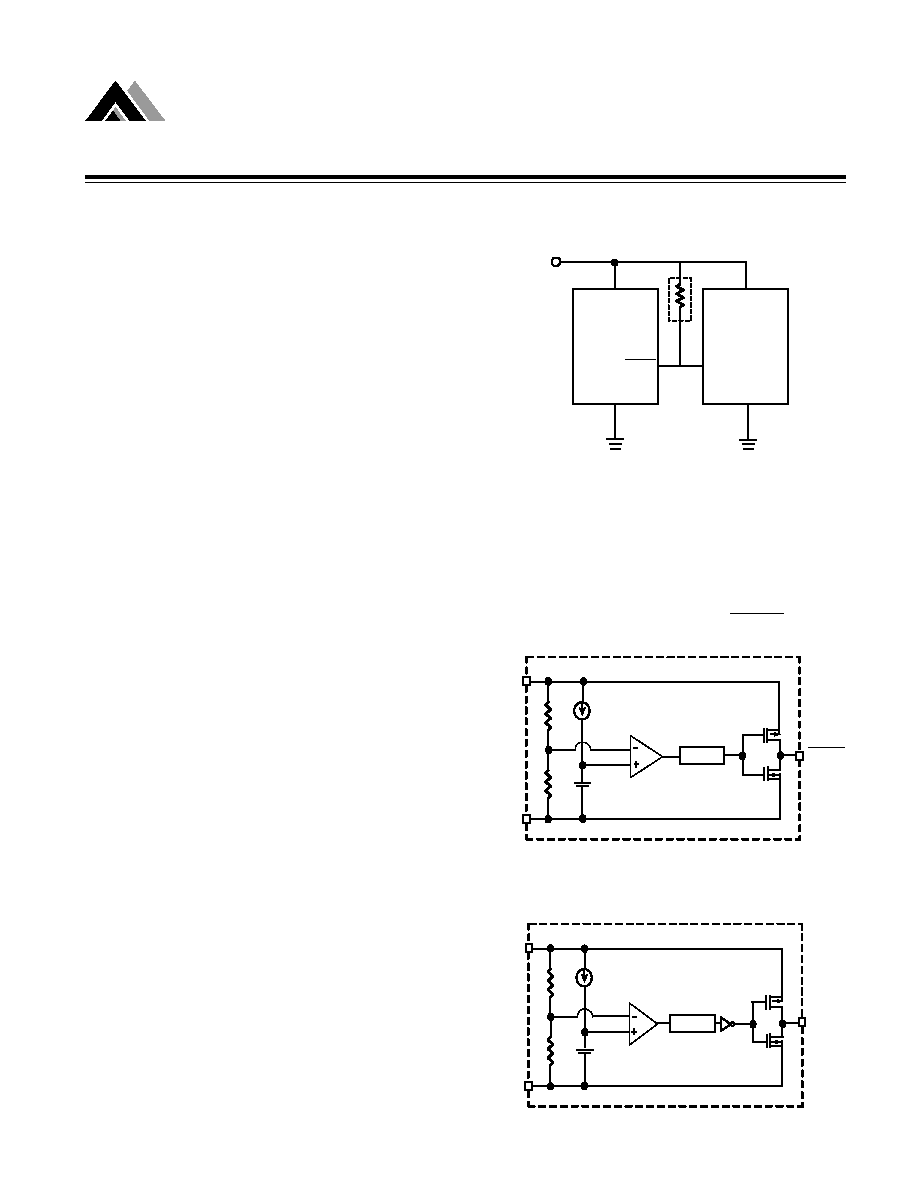
Typical Operating Circuit
Note: * External pull-up resistor is required if open-
drain output is used. 10 k
is recommended.
n
Block Diagram
l
Portable electronics
l
Power supplies
l
Computer peripherals
l
Data acquisition systems
l
Applications using CPUs
l
Consumer electronics
n
Applications
AME8500 with Push-Pull RESET
RESET
V
DD
GND
R1
R2
I1
V
REF
P1
N1
Delay
V
DD
GND
R1
R2
I1
V
REF
P1
N1
RESET
Delay
AME8500 with Push-Pull RESET
Processor
V
CC
GND
RESET
Input
AME8500
V
CC
GND
RESET / RESET
2
3
*
AME, Inc.
2
µµ
µµ
µ
Processor Supervisory
AME8500 / 8501
n
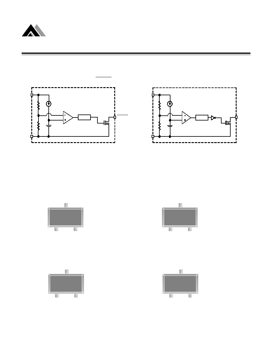
Block Diagram (contd.)
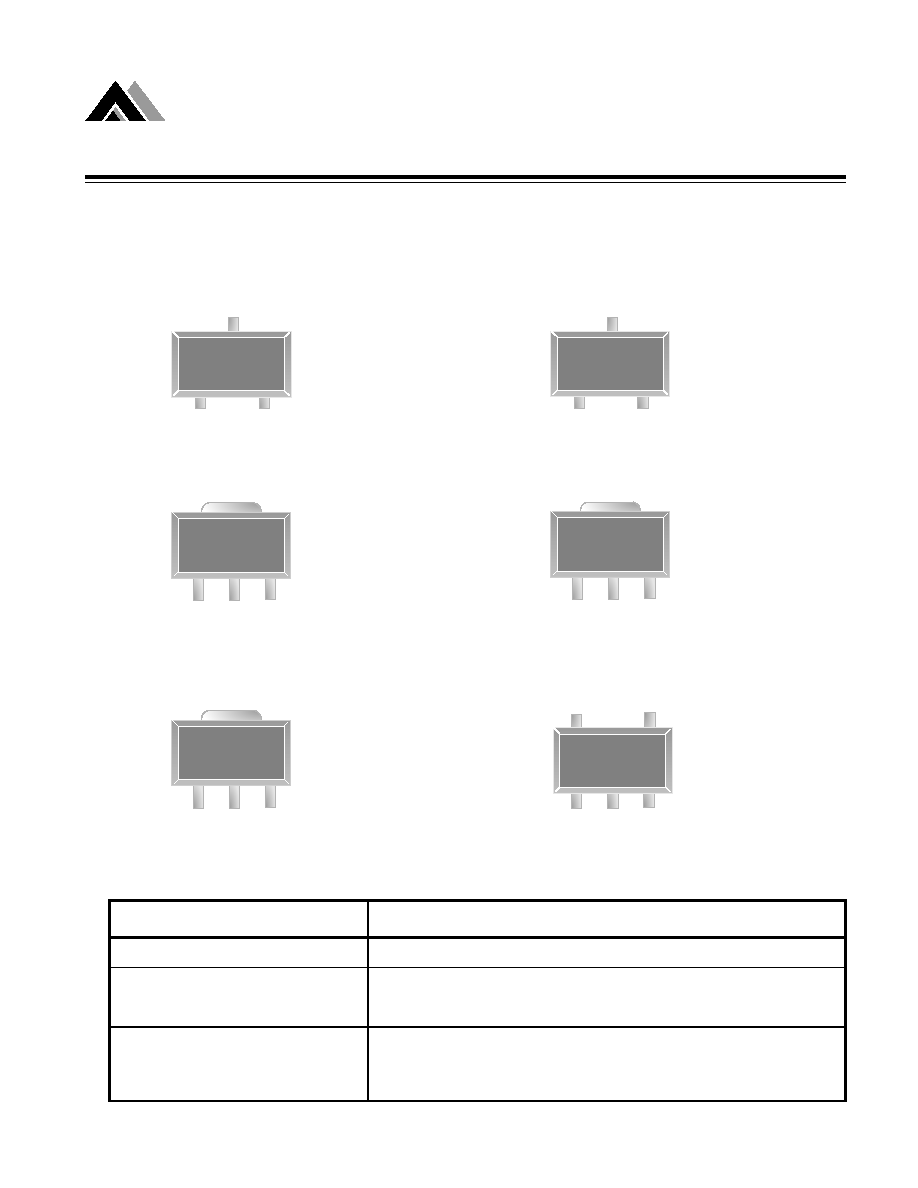
AME8500AEET
AME8501AEET
1. GND
2. Reset/ResetB
3. V
DD
SOT-23
Top View
1
2
3
AME8500
n
Pin Configuration
SOT-23
Top View
1
2
3
AME8500
SOT-23
Top View
AME8500CEET
AME8501CEET
1. Reset/ResetB
2. V
DD
3. GND
1
2
3
AME8500
AME8500BEET
AME8501BEET
1. Reset/ResetB
2. GND
3. V
DD
AME8500 with Open-Drain RESET
Delay
V
DD
GND
R1
R2
I1
V
REF
N1
RESET
AME8500 with Open-Drain RESET
RESET
Delay
V
DD
GND
R1
R2
I1
V
REF
N1
AME8500AEET
AME8501AEET
1. GND
2. Reset/ResetB
3. V
DD
SOT-23-L
Top View
1
2
3
AME8500
AME, Inc.
3
AME8500 / 8501
µµ
µµ
µ
Processor Supervisory
n
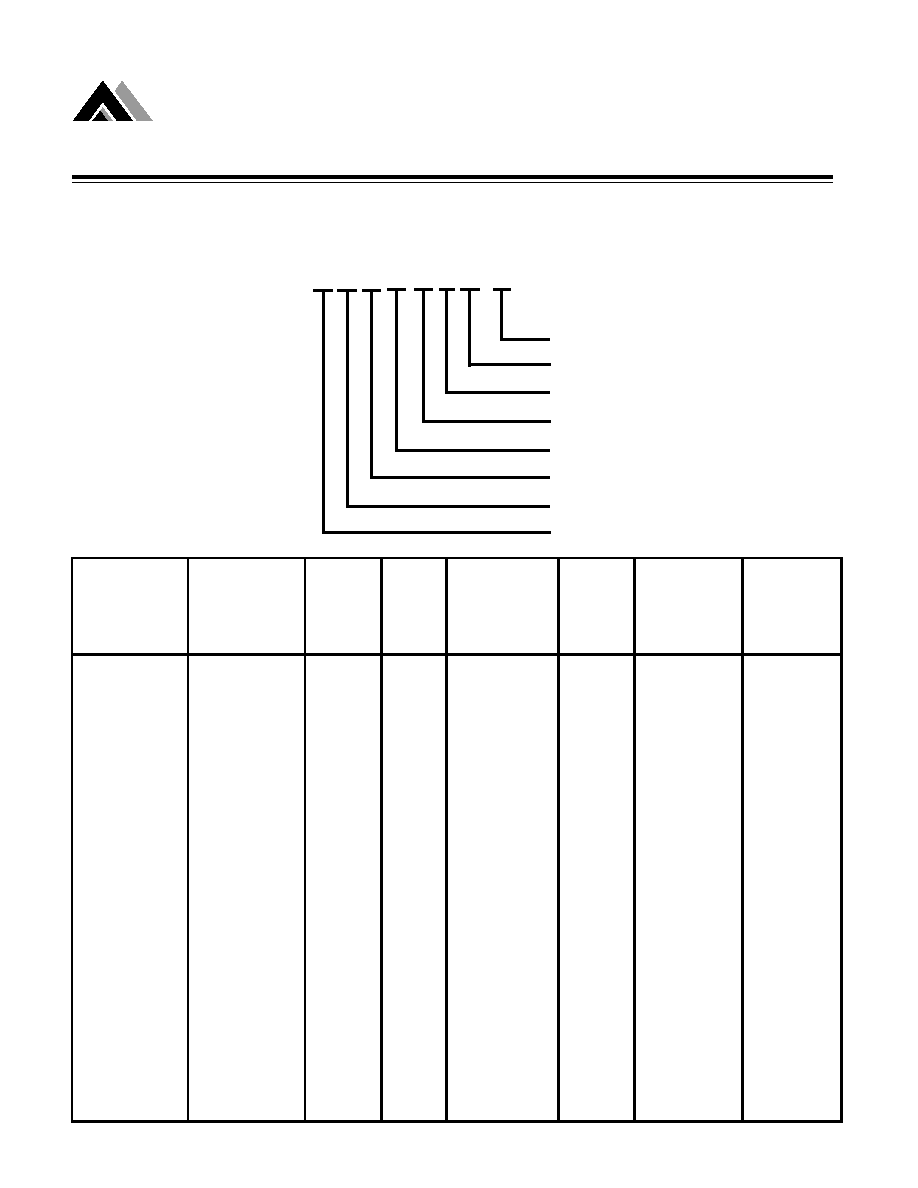
Pin Configuration (contd.)
SOT-89
Top View
SOT-89
Top View
SOT-89
Top View
AME8500AEFT
AME8501AEFT
1. GND
2. V
DD
3. Reset/ResetB
AME8500CEFT
AME8501CEFT
1. V
DD
2. GND
3. Reset/ResetB
AME8500BEFT
AME8501BEFT
1. Reset/ResetB
2. V
DD
3. GND
1
3
2
AME8500
1
3
2
AME8500
1
3
2
AME8500
n
Pin Description
Pin Name
Pin Description
GND
Ground
RESETB/RESET
This pin can be ordered as RESET or RESETB. RESET is active high.
RESETB is active low. It is also available with an open drain or pushpull
output.
V
DD
Positive power supply. A reset is asserted after this voltage drops below
a predetermined level. After V
DD
rises above that level the reset output
remains asserted until the end of the reset timeout period.
SOT-23-L
Top View
AME8500BEET
AME8501BEET
1. Reset/ResetB
2. GND
3. V
DD
1
2
3
AME8500
SOT-23-L
Top View
AME8500CEET
AME8501CEET
1. Reset/ResetB
2. V
DD
3. GND
1
2
3
AME8500
SOT-25
Top View
AME8500BEEV
AME8501BEEV
1. Reset/ResetB
2. V
DD
3. GND
4. N/C
5. N/C
1
3
2
5
4
AME8500
AME, Inc.
4
µµ
µµ
µ
Processor Supervisory
AME8500 / 8501
n
Ordering Information
Operating Temperature Range
Number of Pins
Package Type
Pin Configuration
Special Feature
AME8501 x x
x
x x x
x
x
Output Driver Option
Reset Time (T
D2NOM
)
VDD Threshold Voltage (V
TH
)
AME8500 x x
x
x x x
x
x
A
1. GND
E: -40
O
C to 85
O
C E: SOT-2X
T: 3
A: RESETB /PP A: 1.5 ms
15: VTH= 1.5V
L: Low profile
(SOT-23)
2. Reset/
F: SOT-89
V: 5
B: RESETB /OD D: 30 ms
16: VTH= 1.6V
Y:
ResetB
C: RESET/ PP
E: 150 ms 18: VTH= 1.8V
3. VDD
D: RESET/ OD
F: 210 ms 19: VTH= 1.9V
Z: Lead free
B
1. Reset/
20: VTH= 2.0V
(SOT-23)
ResetB
21: VTH= 2.1V
2. GND
22: VTH= 2.2V
3. VDD
23: VTH= 2.32V
C
1. Reset/
24: VTH= 2.4V
(SOT-23)
ResetB
26: VTH= 2.63V
2. VDD
27: VTH= 2.7V
3. GND
28: VTH= 2.8V
A
1. GND
29: VTH= 2.93V
(SOT-89)
2. VDD
31: VTH= 3.08V
3. Reset/
40: VTH= 4.0V
ResetB
42: VTH= 4.2V
B
1. Reset/
44: VTH= 4.38V
(SOT-89)
ResetB
46: VTH= 4.63V
2. VDD
3. GND
C
1. VDD
(SOT-89)
2. GND
3. Reset/
ResetB
Lead free &
Low profile
Output Driver
Option
Characteristic
of RESET or
RESETB pin
Special
Feature
Reset
Time
(T
D2NOM
)
VDD
Threshold
Voltage (V
TH
)
Package
Type
Number
of
Pins
Operating
Temperature
Range
Pin
Configuration
(PP = Push pull out)
(RESET = Active High)
(RESETB = Active Low)
(OD = Open drain output
polarity)
AME, Inc.
5
AME8500 / 8501
µµ
µµ
µ
Processor Supervisory
n
Ordering Information
Part Number
Marking
V
TH
Voltage
Package
Operating Temp. Range
AME8500AEETAA21
ASVww
2.10V
SOT-23
- 40
o
C to + 85
o
C
AME8500AEETAD20
ALXww
2.00V
SOT-23
- 40
o
C to + 85
o
C
AME8500AEETAE20
AUAww
2.00V
SOT-23
- 40
o
C to + 85
o
C
AME8500AEETAE21
AVGww
2.10V
SOT-23
- 40
o
C to + 85
o
C
AME8500AEETAE26
ASJww
2.63V
SOT-23
- 40
o
C to + 85
o
C
AME8500AEETAE26L
ASJww
2.63V
SOT-23
- 40
o
C to + 85
o
C
AME8500AEETAE29
ALYww
2.93V
SOT-23
- 40
o
C to + 85
o
C
AME8500AEETAE31
AUBww
3.08V
SOT-23
- 40
o
C to + 85
o
C
AME8500AEETAE46
ATSww
4.63V
SOT-23
- 40
o
C to + 85
o
C
AME8500AEETAF15
ATDww
1.50V
SOT-23
- 40
o
C to + 85
o
C
AME8500AEETAF16
ATEww
1.60V
SOT-23
- 40
o
C to + 85
o
C
AME8500AEETAF21
ASKww
2.10V
SOT-23
- 40
o
C to + 85
o
C
AME8500AEETAF23
ATTww
2.32V
SOT-23
- 40
o
C to + 85
o
C
AME8500AEETAF26
AMPww
2.63V
SOT-23
- 40
o
C to + 85
o
C
AME8500AEETAF27
ATRww
2.70V
SOT-23
- 40
o
C to + 85
o
C
AME8500AEETAF29
AMOww
2.93V
SOT-23
- 40
o
C to + 85
o
C
AME8500AEETAF31
ASAww
3.08V
SOT-23
- 40
o
C to + 85
o
C
AME8500AEETAF40
ASBww
4.00V
SOT-23
- 40
o
C to + 85
o
C
AME8500AEETAF44
ARNww
4.38V
SOT-23
- 40
o
C to + 85
o
C
AME8500AEETAF46
ARKww
4.63V
SOT-23
- 40
o
C to + 85
o
C
AME8500AEETBF31
AUTww
3.08V
SOT-23
- 40
o
C to + 85
o
C
AME8500AEETBF46
AUUww
4.63V
SOT-23
- 40
o
C to + 85
o
C
AME8500AEETCA21
ASWww
2.10V
SOT-23
- 40
o
C to + 85
o
C
AME8500AEETCA27
AVBww
2.70V
SOT-23
- 40
o
C to + 85
o
C
AME8500AEETCA46
AVCww
4.63V
SOT-23
- 40
o
C to + 85
o
C
AME8500AEETCD20
ALZww
2.00V
SOT-23
- 40
o
C to + 85
o
C
AME8500AEETCF21
ATYww
2.10V
SOT-23
- 40
o
C to + 85
o
C
AME8500AEETCF29
ALVww
2.93V
SOT-23
- 40
o
C to + 85
o
C
AME8500AEETCF31
ASUww
3.08V
SOT-23
- 40
o
C to + 85
o
C
AME, Inc.
6
µµ
µµ
µ
Processor Supervisory
AME8500 / 8501
n
Ordering Information (contd.)
Part Number
Marking
V
TH
Voltage
Package
Operating Temp. Range
AME8500AEETCF46
ARJww
4.63V
SOT-23
- 40
o
C to + 85
o
C
AME8500AEETDF46
ARIww
4.63V
SOT-23
- 40
o
C to + 85
o
C
AME8500AEFTAA21
A8500A
AA21ww
2.10V
SOT-89
- 40
o
C to + 85
o
C
AME8500AEFTAF27
A8500A
AF27ww
2.70V
SOT-89
- 40
o
C to + 85
o
C
AME8500AEFTCA21
A8500A
CA21ww
2.10V
SOT-89
- 40
o
C to + 85
o
C
AME8500AEFTDA21
A8500A
DA21ww
2.10V
SOT-89
- 40
o
C to + 85
o
C
AME8500BEETAA21
ARTww
2.10V
SOT-23
- 40
o
C to + 85
o
C
AME8500BEETAA27
ARMww
2.70V
SOT-23
- 40
o
C to + 85
o
C
AME8500BEETAA28
ASRww
2.80V
SOT-23
- 40
o
C to + 85
o
C
AME8500BEETAA29
ARZww
2.93V
SOT-23
- 40
o
C to + 85
o
C
AME8500BEETAF27
AUCww
2.70V
SOT-23
- 40
o
C to + 85
o
C
AME8500BEETAF29
AUVww
2.93V
SOT-23
- 40
o
C to + 85
o
C
AME8500BEETAF31
ATOww
3.08V
SOT-23
- 40
o
C to + 85
o
C
AME8500BEETAF40
ATQww
4.00V
SOT-23
- 40
o
C to + 85
o
C
AME8500BEETBA21
AUWww
2.10V
SOT-23
- 40
o
C to + 85
o
C
AME8500BEETBA22
AVDww
2.20V
SOT-23
- 40
o
C to + 85
o
C
AME8500BEETBA24
AUXww
2.40V
SOT-23
- 40
o
C to + 85
o
C
AME8500BEETBA27
ASQww
2.70V
SOT-23
- 40
o
C to + 85
o
C
AME8500BEETBA28
ASSww
2.80V
SOT-23
- 40
o
C to + 85
o
C
AME8500BEETBA28L
ASSww
2.80V
SOT-23
- 40
o
C to + 85
o
C
AME8500BEETBA28Y
ASSww
2.80V
SOT-23
- 40
o
C to + 85
o
C
AME8500BEETBA29
ARLww
2.93V
SOT-23
- 40
o
C to + 85
o
C

AME, Inc.
7
AME8500 / 8501
µµ
µµ
µ
Processor Supervisory
n
Ordering Information (contd.)
Part Number
Marking
V
TH
Voltage
Package
Operating Temp. Range
AME8500BEETBA42
ASIww
4.20V
SOT-23
- 40
o
C to + 85
o
C
AME8500BEETCA21
ASXww
2.10V
SOT-23
- 40
o
C to + 85
o
C
AME8500BEEVAK27
AUFww
2.70V
SOT-25
- 40
o
C to + 85
o
C
AME8500BEFTAA21
A8500B
AA21ww
2.10V
SOT-89
- 40
o
C to + 85
o
C
AME8500BEFTAA27
A8500B
AA27ww
2.70V
SOT-89
- 40
o
C to + 85
o
C
AME8500BEFTAF27
A8500B
AF27ww
2.70V
SOT-89
- 40
o
C to + 85
o
C
AME8500BEFTAF40
A8500B
AF40ww
4.00V
SOT-89
- 40
o
C to + 85
o
C
AME8500BEFTBA23
A8500B
BA23ww
2.32V
SOT-89
- 40
o
C to + 85
o
C
AME8500CEETAA21
ASYww
2.10V
SOT-23
- 40
o
C to + 85
o
C
AME8500CEETAE26
ASHww
2.63V
SOT-23
- 40
o
C to + 85
o
C
AME8500CEETAE42
AUZww
4.20V
SOT-23
- 40
o
C to + 85
o
C
AME8500CEETAF29
ASLww
2.93V
SOT-23
- 40
o
C to + 85
o
C
AME8500CEETBE42
AVAww
4.20V
SOT-23
- 40
o
C to + 85
o
C
AME8500CEETBF31
AVYww
3.08V
SOT-23
- 40
o
C to + 85
o
C
AME8500CEETBF46
ARWww
4.63V
SOT-23
- 40
o
C to + 85
o
C
AME8500CEETCA21
ASZww
2.10V
SOT-23
- 40
o
C to + 85
o
C
AME8500CEFTBA27
A8500C
BA27ww
2.70V
SOT-89
- 40
o
C to + 85
o
C
AME8500CEFTBA29
A8500C
BA29ww
2.93V
SOT-89
- 40
o
C to + 85
o
C
AME8500CEFTBA42
A8500C
BA42ww
4.20V
SOT-89
- 40
o
C to + 85
o
C
AME8500CEFTCD28
A8500C
CD28ww
2.80V
SOT-89
- 40
o
C to + 85
o
C
AME8500CEFTCD46
A8500C
CD46ww
4.63V
SOT-89
- 40
o
C to + 85
o
C
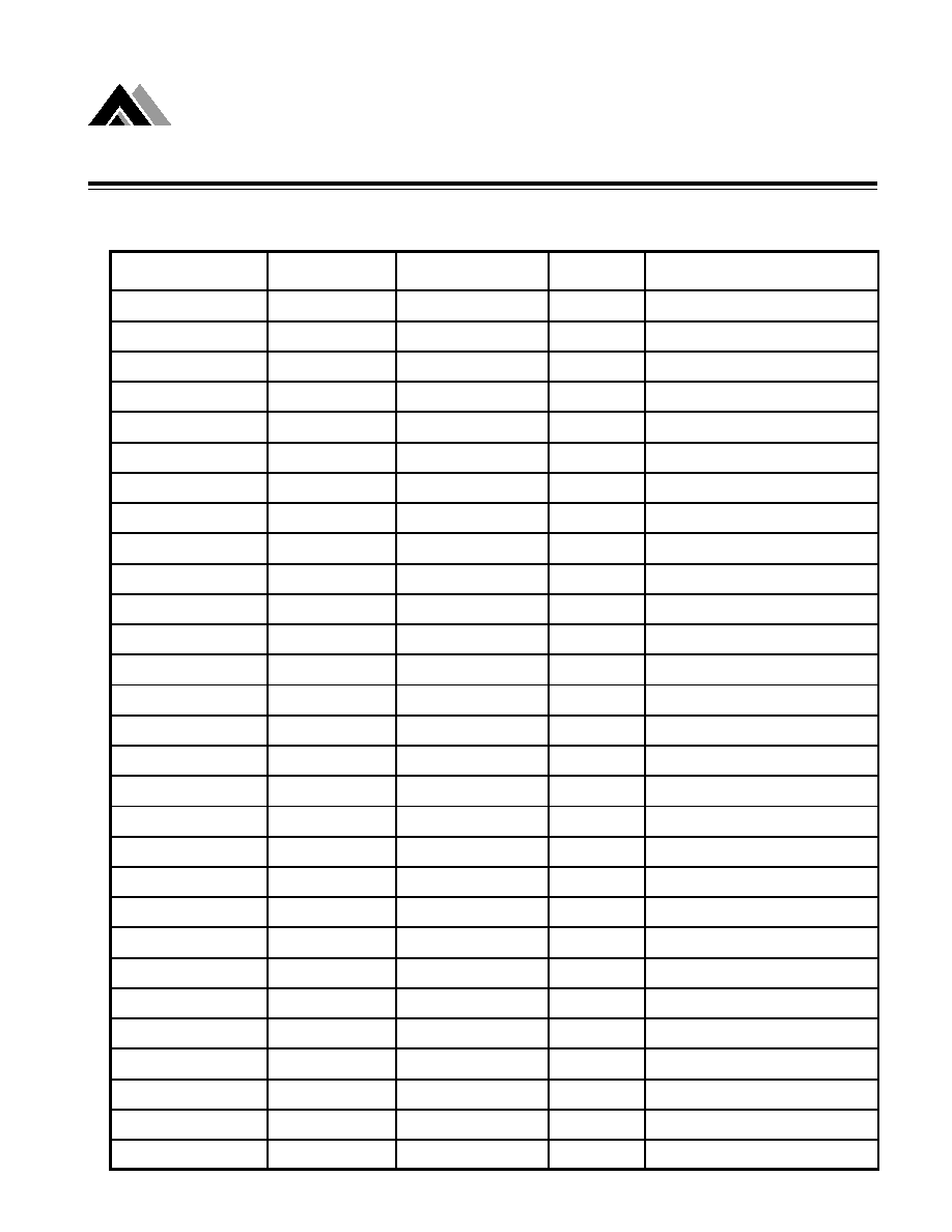
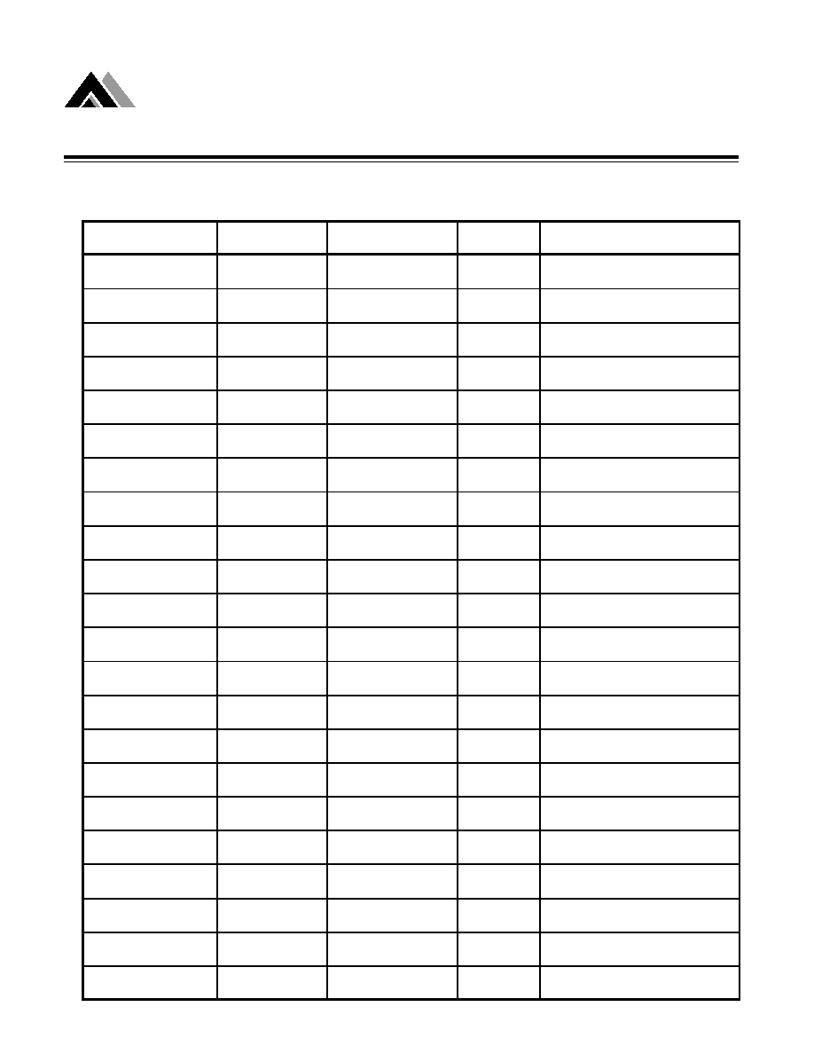
Please consult AME sales office or authorized Rep./Distributor for other voltage options.
AME, Inc.
8
µµ
µµ
µ
Processor Supervisory
AME8500 / 8501
Maximum
Unit
SOT-23
325
SOT-89
180
SOT-23
350
SOT-89
650
150
o
C
300
o
C
o
C / W
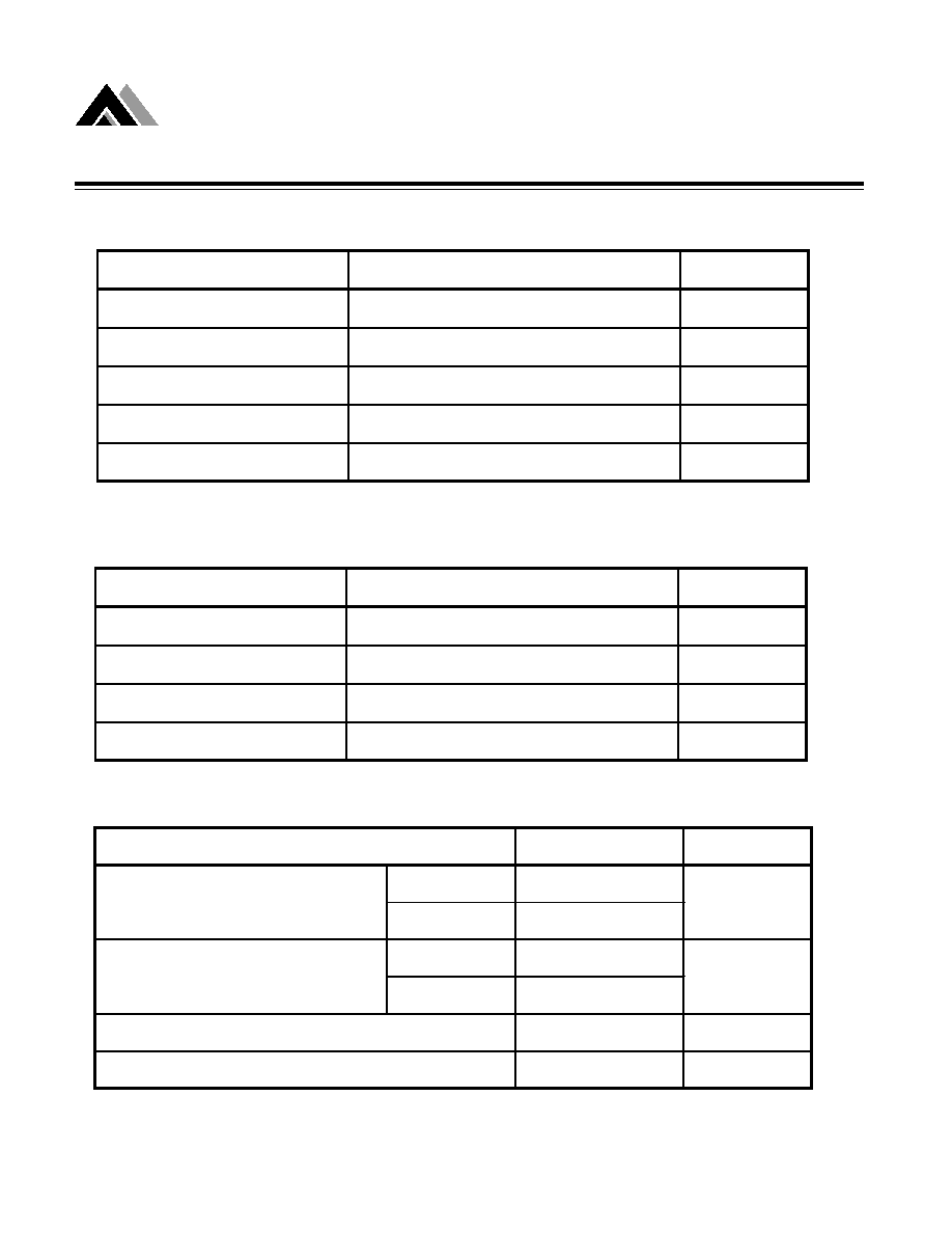
Parameter
Thermal Resistance
Maximum Junction Temperature
Maximum Lead Temperature (10 Sec)
Power Dissipation
mW
Parameter
Rating
Unit
Supply Voltage
1.6 - 5
V
Ambient Temperature Range
- 40 to + 85
o
C
Junction Temperature
- 40 to + 125
o
C
Storage Temperature
- 65 to 150
o
C
Parameter
Maximum
Unit
Supply Voltage
7
V
ESD Classification
B
Input Current, V
DD
20
mA
Output Current, RESET, ResetB
20
mA
Rate of Rise, V
DD
100
V/
µ
s
n
Absolute Maximum Ratings
n
Recommended Operating Conditions
n
Thermal Information
Caution: Stress above the listed absolute maximum rating may cause permanent damage to the device
AME, Inc.
9
AME8500 / 8501
µµ
µµ
µ
Processor Supervisory
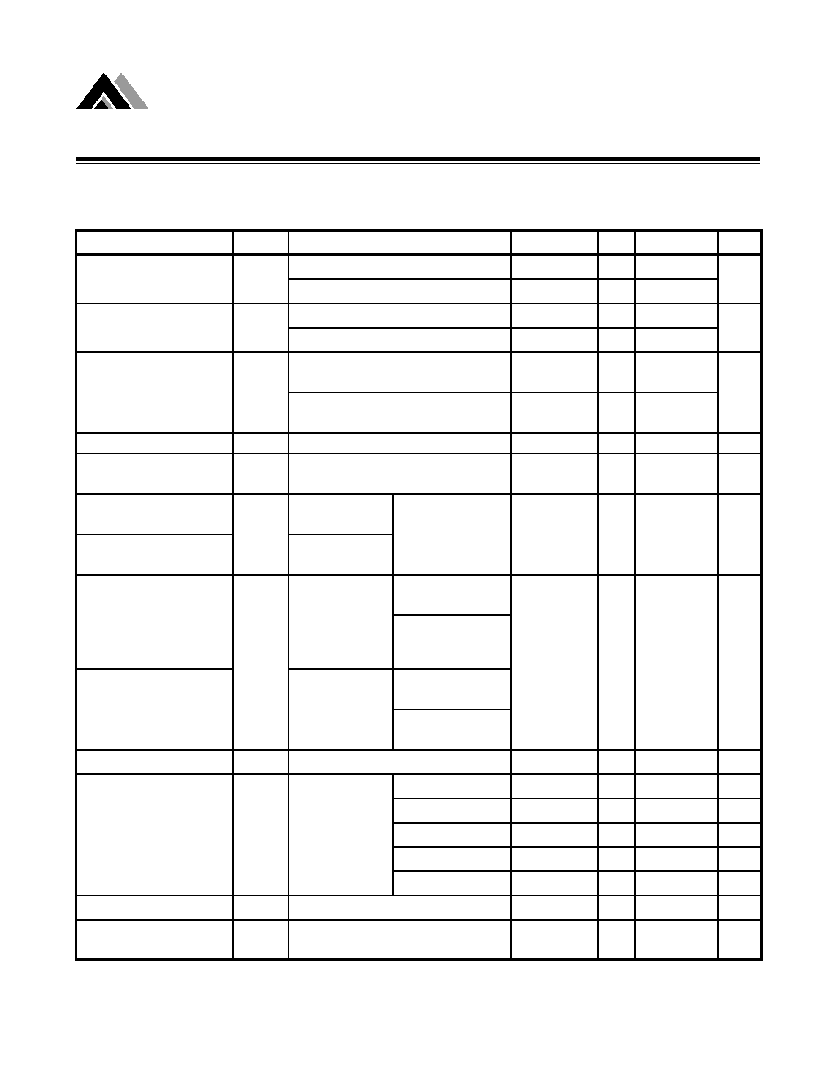
Parameter
Symbol
Min
Typ
Max
Units
1
5.5
1
5.5
3.0
5.0
V
THNOM
-
1.5%
V
THNOM
+
1.5%
V
THNOM
-
2.0%
V
THNOM
+
2.0%
Hysteresis Range
V
HY ST
20
mV
RESET Threshold
Tempco
30
ppm
RESETB Output
Voltage Low
V
DD
<V
TH (MIN)
RESET Output
Voltage Low
V
DD
>V
TH (MAX)
I
SOURCE
=0.5mA,
V
DD
>1.8V
I
SOURCE
=0.15mA,
1.8V>=V
DD
>1.0V
I
SOURCE
=0.5mA,
V
DD
>1.8V
I
SOURCE
=0.15mA,
1.8V>=V
DD
>1.0V
V
DD
to Reset Delay
T
D1
40
200
µ
S
Version A
0.5
1.5
5
mS
Version D
15
30
50
mS
Version E
80
150
230
mS
Version F
140
210
500
mS
Version K
300
440
600
mS
Temperature Shutdown
T
OFF
80
o
C
Temperature Shutdown
Hysteresis
T
HY S
20
o
C
V
V
OL
0.8V
DD
mV
I
SINK
=1.2mA,
TA= -40~85
o
C
0.5
V
V
Supply Current
I
DD
TA=-40~85
o
C
µ
A
V
DD
= V
TH
*1.10
V
DD
=
V
TH
*1.10, TA=-40~85
o
C
Test Condition
TA=-40~85
o
C
V
RELEASE
- V
TH
, note1
V
TH
Reset Threshold
V
DD
Range*
V
RANGE
AME8501 only
AME8501 only
V
DD
= V
TH
- 100mV, TA= -40 ~ 85
o
C
Reset Timeout Period*
T
D2
TA= -40 ~ 85
o
C
RESETB Output
Voltage High
V
DD
>V
TH (MAX)
RESET Output
Voltage High
V
OH
V
DD
<V
TH (MIN)
n
Electrical Specifications
TA = 25
O
C unless otherwise noted
Note1:The data based on V
TH
=2.7V part type.
AME, Inc.
10
µµ
µµ
µ
Processor Supervisory
AME8500 / 8501
n
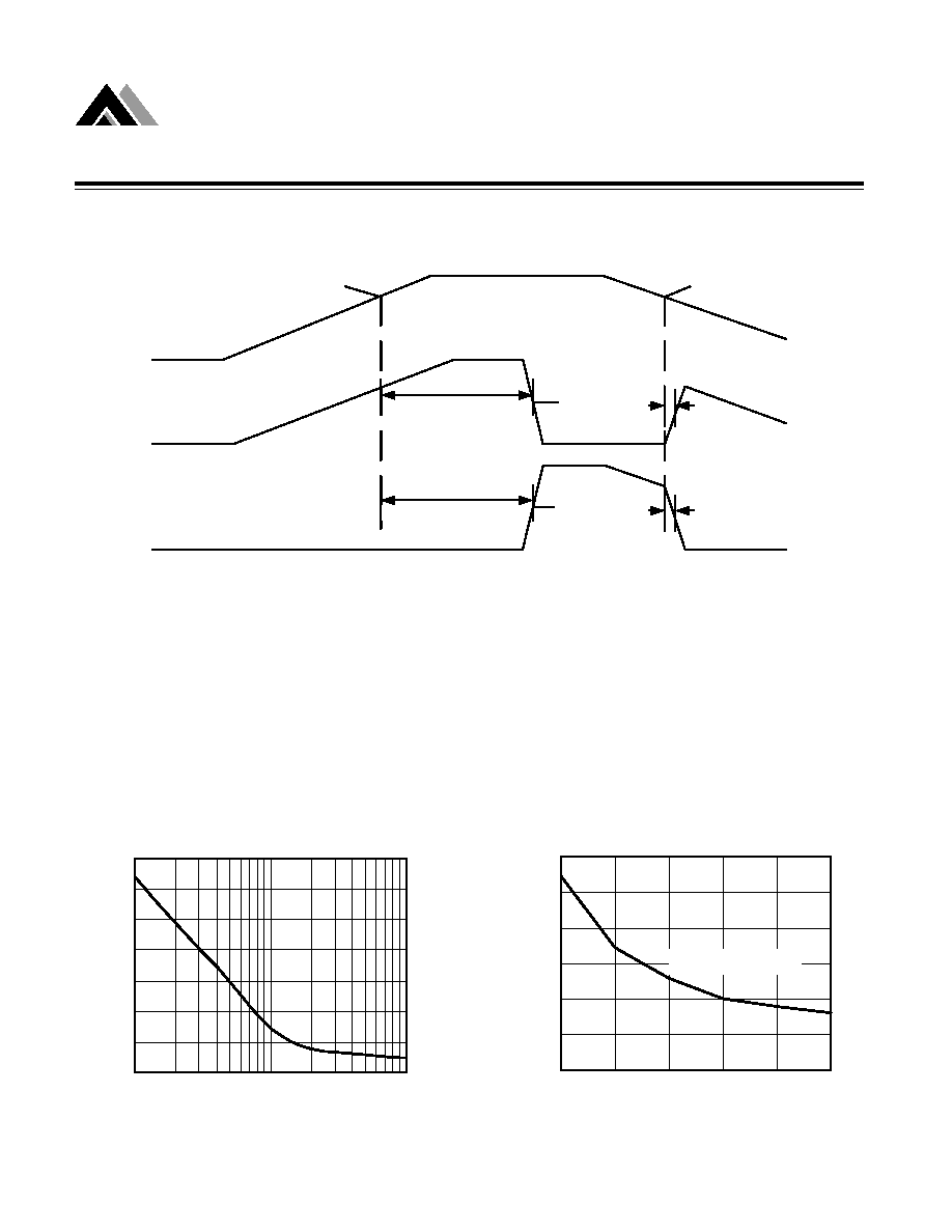
Timing Diagram
n
Applications Information
Supply Transients
These devices have a certain immunity to fast negative
going transients. In the following pages the graph titled
"Glitch Rejection" indicates the maximum allowable glitch
amplitude and duration to avoid triggering an unintended
reset. As shown in the graph shorter transients can have
larger amplitudes without triggering resets.
V
DD
RESETB
RESET
T
D2
V
Release
V
TH
T
D1
T
D2
T
D1
50%
50%
50%
50%
Glitch Rejection
Reset Time vs. Temperature
G
l
i
t
ch
Du
rati
on (
µ
µ
µ
µ
S)
Glitch Amplitude (V)
0
20
40
60
80
100
120
140
0.01
0.1
1
Re
set Ti
m
e
(
m
S
)
190
195
200
205
210
215
220
-45
-5
25
55
85
115
Temperature (
o
C)
AME8500AEETAF26

AME, Inc.
11
AME8500 / 8501
µµ
µµ
µ
Processor Supervisory
I
DD
vs. V
DD
Threshold Hysteresis vs. Temperature
T
D1
Delay vs. Temperature
I
DD
vs. Temperature
Reset V
TH
vs. Temperature
Reset VOL vs. Temperature
Suppl
y
C
u
r
r
en
t
@ 5V (u
A)
Temperature (
o
C)
2.10
2.15
2.20
2.25
2.30
2.35
-45
-5
25
55
85
115
AME8500AEETAF26
2.630
2.632
2.634
2.636
2.638
2.640
2.642
2.644
2.646
2.648
2.650
-45
-5
25
55
85
115
Re
set V
t
h (
V
)
Temperature (
o
C)
AME8500AEETAF26
I
DD
(uA
)
V
DD
(V)
0
0.4
0.8
1.2
1.6
2
0
1
2
3
4
5
85
O
C
-40
O
C
0
O
C
TD2
De
lay (
u
S
)
Temperature (
o
C)
37
38
39
40
41
42
43
-40
-20
0
20
40
60
80
100
Hy
stere
s
i
s (
%
o
f
V
TH
)
Temperature (
o
C)
0
0.1
0.2
0.3
0.4
0.5
-40
-20
0
20
40
60
80
100
0.220
0.225
0.230
0.235
0.240
0.245
0.250
0.255
0.260
0.265
-45
-5
25
55
85
115
Reset
VO
L
@ 0.8
m
A (
V
)
Temperature (
o
C)
AME8500AEETAF26
AME, Inc.
12
µµ
µµ
µ
Processor Supervisory
AME8500 / 8501
MIN
MAX
MIN
MAX
A+A
1
1.00
1.30
0.0394
0.0512
b
0.35
0.50
0.0138
0.0197
C
0.09
0.25
0.0035
0.0098
D
2.70
3.10
0.1063
0.1220
E
1.40
1.80
0.0551
0.0709
e
H
2.40
3.00
0.09449 0.11811
L
Ë1
0
o
10
o
0
o
10
o
1.90 BSC
0.0748 BSC
0.35BSC
0.0138BSC
SYMBOLS
MILLIMETERS
INCHES
n
Package Dimension
SOT-23
MIN
MAX
MIN
MAX
A
1.00
1.40
0.0394
0.0551
A
1
0.00
0.15
0.0000
0.0059
b
0.35
0.50
0.0138
0.0197
C
0.09
0.25
0.0035
0.0098
D
2.70
3.10
0.1063
0.1220
E
1.40
1.80
0.0551
0.0709
e
H
2.40
3.00
0.09449 0.11811
L
Ë1
0
o
10
o
0
o
10
o
SYMBOLS
MILLIMETERS
INCHES
1.90 BSC
0.0748 BSC
0.35BSC
0.0138BSC
b
£ c
1
C
D
H
E
e
L
A
A1
Top View
Side View
Front View
SOT-23-L
b
£ c
1
C
D
H
E
e
L
A
A1
Top View
Side View
Front View
AME, Inc.
13
AME8500 / 8501
µµ
µµ
µ
Processor Supervisory
n
Package Dimension
SOT-89
MIN
MAX
MIN
MAX
A
1.39
1.60
0.05472 0.06299
A
1
C
0.35
0.44
0.01378 0.01732
D
4.39
4.60
0.17283
0.1811
D
1
1.35
1.83
0.05315 0.07205
E
2.28
3.60
0.08976 0.14173
e
H
S1
3.00REF
0.70REF
1.50REF
0.1181REF
0.0276REF
0.0590REF
0.8REF
0.0315REF
SYMBOLS
MILLIMETERS
INCHES
A
H
A1
Top View
Side View
Front View
D
D1
E
e
C
POLISH
POLISH
MATTE FINISH
S1
SOT-25
MIN
MAX
MIN
MAX
A
A
1
0.00
0.15
0.0000
0.0059
b
0.30
0.55
0.0118
0.0217
D
2.70
3.10
0.1063
0.1220
E
1.40
1.80
0.0551
0.0709
e
H
2.60
3.00
0.10236 0.11811
L
Ë1
0
o
10
o
0
o
10
o
S
1
0.37BSC
0.0146BSC
0.95BSC
0.0374BSC
1.90 BSC
0.07480 BSC
SYMBOLS
MILLIMETERS
INCHES
1.20REF
0.0472REF
L
Top View
Side View
Front View
£ c
1
D
S1
e
E
H
A1
b
A

Life Support Policy:
These products of AME, Inc. are not authorized for use as critical components in life-support devices or
systems, without the express written approval of the president
of AME, Inc.
AME, Inc. reserves the right to make changes in the circuitry and specifications of its devices and
advises its customers to obtain the latest version of relevant information.
©
AME, Inc. , June 2003
Document: 2007-DS8500/8501-L
Corporate Headquarter
U.S.A. Subsidiary
AME, Inc. Analog Microelectronics, Inc.
2F, 189 Kang-Chien Road, Nei-Hu Dist. 3100 De La Cruz Blvd., Suite 201
Taipei 114 Taiwan, R.O.C. Santa Clara, CA. 95054-2046
Tel: 886 2 2627-8687 Tel : (408) 988-2388
Fax: 886 2 2659-2989
Fax: (408) 988-2489
www.ame.com.tw
E-Mail: sales@ame.com.tw