Windows is a registered trademark of Microsoft Corporation. American Microsystems, Inc. reserves the right to change the detail specifications as may be required to permit improvements in the
design of its products.
3.4.02
FS6011-02
FS6011-02
FS6011-02
FS6011-02
Digital Audio/Video Clock Generator IC
Digital Audio/Video Clock Generator IC
Digital Audio/Video Clock Generator IC
Digital Audio/Video Clock Generator IC
ISO9001
ISO9001
ISO9001
ISO9001
1.0 Features
�
Triple phase-locked loop (PLL) device provides exact
ratiometric derivation of Audio, Processor, and Utility
Clocks
�
On-chip tunable voltage-controlled crystal oscillator
(VCXO) allows precise system frequency tuning
�
Serial interface for Audio and Utility Clock frequency
selection
�
Board-programmable Processor Clock frequency
selection
�
Supports 32, 44.1, and 48kHz 256x oversampled
DACs as well as 384x at 44.1kHz and 512x at 48kHz
�
Tunable Audio Clock frequencies for undetectable
resynchronization of audio and video streams
�
Small circuit board footprint (16-pin 0.150
SOIC)
�
Custom frequency selections available - contact your
local AMI Sales Representative for more information
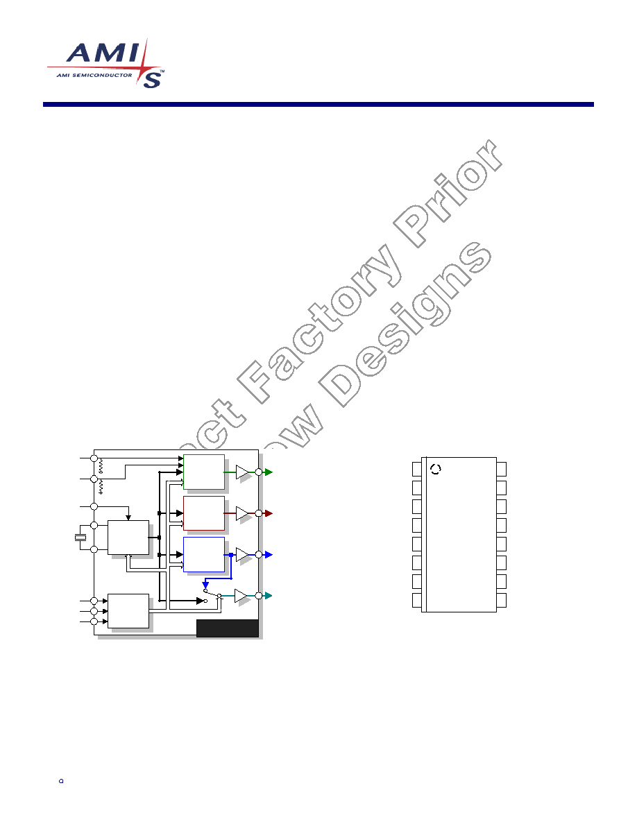
Figure 1: Block Diagram
VCXO
Serial
Interface
SDATA
SCLK
SLOAD
FS6011
UCLK
Processor
Clock PLL
Audio
Clock PLL
Utility
Clock PLL
XOUT
XIN
CLK_27
ACLK
PCLK
XTUNE
PSEL1
PSEL0
2.0 Description
The FS6011-02 is a monolithic CMOS clock generator IC
designed to minimize cost and component count in digital
video/audio systems.
At the core of the FS6011-02 is circuitry that implements
a voltage-controlled crystal oscillator when an external
resonator (nominally 27MHz) is attached. The VCXO al-
lows device frequencies to be precisely adjusted for use
in systems that have frequency matching requirements,
such as digital satellite receivers.
Three high-resolution phase-locked loops independently
generate three other selectable frequencies derived from
the VCXO frequency. These clock frequencies are re-
lated to the VCXO frequency and to each other by exact
ratios. The locking of all the output frequencies together
can eliminate unpredictable artifacts in video systems
and reduce electromagnetic interference (EMI) due to
frequency harmonic stacking.
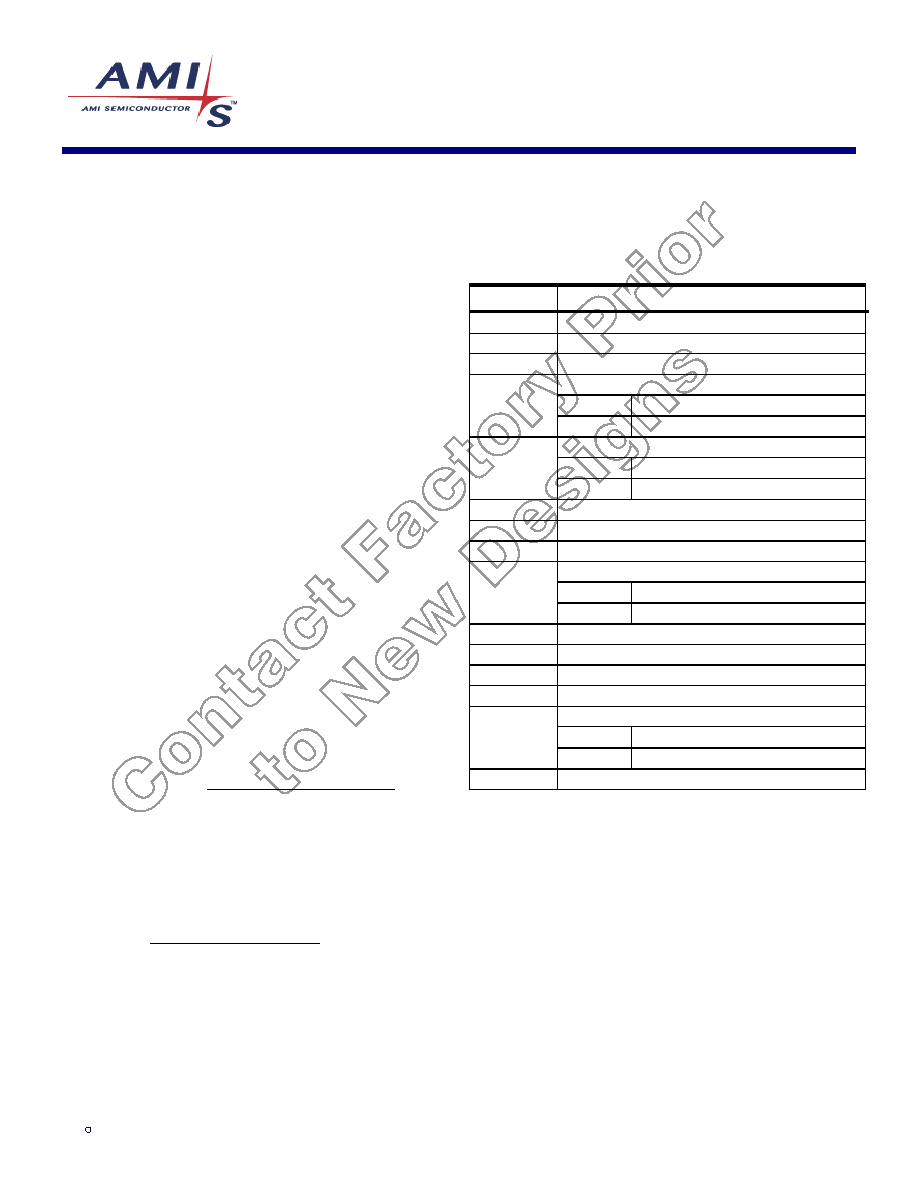
Figure 2: Pin Configuration
1
16
2
3
4
5
6
7
8
15
14
13
12
11
10
9
SCLK
SDATA
SLOAD
VSS
XIN
XOUT
XTUNE
VDD
PSEL1
PSEL0
VSS
PCLK
UCLK
VDD
ACLK
CLK27
FS6011
16-pin (0.150
) SOIC

2
3.4.02
FS6011-02
FS6011-02
FS6011-02
FS6011-02
Digital Audio/Video Clock Generator IC
Digital Audio/Video Clock Generator IC
Digital Audio/Video Clock Generator IC
Digital Audio/Video Clock Generator IC
ISO9001
ISO9001
ISO9001
ISO9001
Table 1: Pin Descriptions
Key: AI = Analog Input; AO = Analog Output; DI = Digital Input; DI
U
= Input with Internal Pull-Up; DI
D
= Input with Internal Pull-Down; DIO = Digital Input/Output; DI-3 = Three-Level Digital Input,
DO = Digital Output; P = Power/Ground; # = Active Low pin
PIN
TYPE
NAME
DESCRIPTION
1
DI
SCLK
Serial Data Clock
2
DI
SDATA
Serial Data Input
3
DI
SLOAD
Serial Port Load
4
P
VSS
Ground
5
AI
XIN
VCXO Feedback
6
AO
XOUT
VCXO Drive
7
AI
XTUNE
VCXO Tune
8
P
VDD
Power Supply (+5V)
9
DI
D
PSEL1
PCLK Select MSB
10
DI
D
PSEL0
PCLK Select LSB
11
P
VSS
Ground
12
DO
PCLK
Processor Clock Output
13
DO
UCLK
Utility Clock Output
14
P
VDD
Power Supply (+5V)
15
DO
ACLK
Audio Clock Output
16
DO
CLK27
Reference Clock Output
3.0 Functional Block Description
3.1 Phase-Locked
Loops
Each of the three on-chip PLLs in the FS6011 multiplies
the reference frequency to the desired frequency by a
ratio of integers. This frequency multiplication is exact.
3.2
Output Tristate Control
All four clock outputs of the FS6011 may be tristated to
facilitate circuit board testing. To place the outputs in
tristate mode, follow this sequence:
1. force XIN low (i.e. ground)
2. apply power to the device
3. wait until the internal power-on reset has deasserted
4. apply a negative-going transition to the PSEL0 pin
Outputs may be re-enabled by removing and reapplying
power to the FS6011. To re-enable outputs without re-
moving power, apply a rising edge transition to the XIN in
and follow it with a falling edge transition on the PSEL0
pin.
3.3 Digital
Interface
Digital data is placed on the SDATA pin and clocked into
the FS6011 internal shift register (D[0] first) with a rising
edge on the SCLK pin. The shift register data is trans-
ferred to the FS6011 control registers with a rising edge
on the SLOAD pin. Fifteen bits must be shifted into the
internal registers before the parallel load can be per-
formed. In addition to the normal control functions per-
formed by D[13:0], there is one reserved bit, D[14], that
should be set to zero.
All control registers are initialized to zero on power-up.
Figure 3: Communications Protocol
SCLK
SDATA
t
hd:DAT
t
LO
t
HI
SLOAD
t
su:DAT
t
R
t
F
t
LO
t
HI
t
su:LD
t
hd:LD
3
3.4.02
FS6011-02
FS6011-02
FS6011-02
FS6011-02
Digital Audio/Video Clock Generator IC
Digital Audio/Video Clock Generator IC
Digital Audio/Video Clock Generator IC
Digital Audio/Video Clock Generator IC
ISO9001
ISO9001
ISO9001
ISO9001
3.4 Voltage-Controlled
Crystal
Oscillator (VCXO)
The VCXO provides a tunable, low-jitter frequency refer-
ence for the rest of the FS6011 system components.
Loading capacitance for the crystal is internal to the
FS6011. No external components (other than the reso-
nator itself) are required for operation of the VCXO.
The resonator loading capacitance is adjustable under
register control. This permits factory coarse tuning of in-
expensive resonators to the necessary precision for digi-
tal video applications. Refer to Section 4.6.
Continuous fine-tuning of the VCXO frequency is accom-
plished by varying the voltage on the XTUNE pin. The
total change (from one extreme to the other) in effective
loading capacitance is 1.5pF nominal.
The oscillator operates the crystal resonator in the paral-
lel-resonant mode. Crystal warping, or the "pulling" of the
crystal oscillation frequency, is accomplished by altering
the effective load capacitance presented to the crystal by
the oscillator circuit. The actual amount that changing the
load capacitance alters the oscillator frequency will be
dependent on the characteristics of the crystal as well as
the oscillator circuit itself.
Specifically, the motional capacitance of the crystal (usu-
ally referred to by crystal manufacturers as C
1
), the static
capacitance of the crystal (C
0
), and the load capacitance
(C
L
) of the oscillator determine the warping capability of
the crystal in the oscillator circuit.
A simple formula to obtain the warping capability of a
crystal oscillator is:
(
)
(
) (
)
C
C
C
C
C
C
C
ppm
f
L
L
L
L
1
0
2
0
6
1
2
1
2
10
)
(
+
�
+
�
�
-
�
=
where C
L1
and C
L2
are the two extremes of the applied
load capacitance.
A crystal with the following parameters is used. With C
1
=
0.02pF, C
0
= 5pF, C
L1
= 10pF, and C
L2
= 22.66pF, the
coarse tuning range is
(
)
(
) (
)
ppm
.
.
.
f
305
10
5
66
22
5
2
106
10
66
22
02
0
=
+
�
+
�
�
-
�
=
.
4.0 Programming
Information
Table 2: Register Summary
BIT D[x]
REGISTER BIT DESCRIPTION
0
ACLK Select (LSB)
1
ACLK Select
2
ACLK Select (MSB)
ACLK Off-Speed Mode
Bit = 0
Disable Off-Speed Mode
3
Bit = 1
Enable Off-Speed Mode
ACLK Speed Control
Bit = 0
Low Speed
4
Bit = 1
High Speed
5
UCLK Select (LSB)
6
UCLK Select
7
UCLK Select (MSB)
CLK27 Select
Bit = 0
Selects VCXO Frequency
8
Bit = 1
Selects UCLK Frequency
9
Crystal Oscillator Coarse Tune (LSB)
10
Crystal Oscillator Coarse Tune
11
Crystal Oscillator Coarse Tune
12
Crystal Oscillator Coarse Tune (MSB)
VCXO Enable/Disable Control
Bit = 0
Disable VCXO Mode
13
Bit = 1
Enable VCXO Mode
14
Reserved (should be set to 0)

4
3.4.02
FS6011-02
FS6011-02
FS6011-02
FS6011-02
Digital Audio/Video Clock Generator IC
Digital Audio/Video Clock Generator IC
Digital Audio/Video Clock Generator IC
Digital Audio/Video Clock Generator IC
ISO9001
ISO9001
ISO9001
ISO9001
4.1
Audio PLL Clock Frequencies (ACLK)
The ACLK frequency is controlled by register bits D[0],
D[1], and D[2] accessed via the serial interface. The
ACLK frequencies listed below are derived via the PLL
Divider Ratio from a reference frequency of 27MHz.
Table 3: ACLK Frequency Select
D[2]
D[1]
D[0]
PLL DIVIDER
RATIO
AUDIO
OVERSAMPLING
ACLK
(MHz)
0
0
0
1024 / 2250
48kHz x 256
12.288
0
0
1
1024 / 3375
32kHz x 256
8.192
0
1
0
1024 / 4500
48kHz x 256 / 2
6.144
0
1
1
1024 / 6750
32kHz x 256 / 2
4.096
1
0
0
1568 / 3750
44.1kHz x 256
11.2896
1
0
1
1568 / 2500
44.1kHz x 384
16.9344
1
1
0
1568 / 7500
44.1kHz x 256 / 2
5.6448
1
1
1
1024 / 1125
48kHz x 512
24.576
NOTE: Contact AMI for custom PLL frequencies
4.2
Audio Clock Off-Speed Frequencies
The ACLK frequencies shown may be smoothly modified
to a slightly higher or lower value under register control.
Register bit D[3] must be a logic-one to activate this
mode. The value of D[4] controls whether the frequency
will be adjusted slightly low (D[4] = 0) or high (D[4] = 1).
Table 4: Audio Off Speed Frequencies
D[4]
D[3]
D[2]
D[1]
D[0]
PLL DIVIDER
RATIO
ACLK
(MHz)
0
1
0
0
0
1023 / 2250
12.276
0
1
0
0
1
1023 / 3375
8.184
0
1
0
1
0
1023 / 4500
6.138
0
1
0
1
1
1023 / 6750
4.092
0
1
1
0
0
1567 / 3750
11.2824
0
1
1
0
1
1567 / 2500
16.9236
0
1
1
1
0
1567 / 7500
5.6412
0
1
1
1
1
1023 / 1125
24.5520
1
1
0
0
0
1025 / 2250
12.3000
1
1
0
0
1
1025 / 3375
8.2000
1
1
0
1
0
1025 / 4500
6.1500
1
1
0
1
1
1025 / 6750
4.1000
1
1
1
0
0
1569 / 3750
11.2968
1
1
1
0
1
1569 / 2500
16.9432
1
1
1
1
0
1569 / 7500
5.6484
1
1
1
1
1
1025 / 1125
24.6000
4.3
Utility PLL Clock Frequencies (UCLK)
The UCLK frequency is controlled by register bits D[5],
D[6] and D[7], accessed via the serial interface. UCLK
frequencies listed below are derived via the PLL Divider
Ratio from a reference frequency of 27MHz.
Table 5: UCLK Frequency Select
D[7]
D[6]
D[5]
PLL DIVIDER RATIO
UCLK (MHz)
0
0
0
16 / 27
16.0000
0
0
1
35 / 33
28.6363
0
1
0
1568 / 3750
11.2896
0
1
1
1
27.0000
1
0
0
544 / 375
39.1680
1
0
1
728 / 375
52.4160
1
1
0
10 / 9
30.0000
1
1
1
1024 / 1125
24.5760
NOTE: Contact AMI for custom PLL frequencies
4.4
Processor PLL Frequencies (PCLK)
The PCLK frequency is controlled by the logic levels on
the PSEL0 and PSEL1 inputs. These inputs have weak
pull-downs. PCLK frequencies listed below are derived
via the PLL Divider Ratio from a reference frequency of
27MHz.
Table 6: PCLK Frequency Select
PSEL1
PSEL0
PLL DIVIDER RATIO
PCLK (MHz)
0
0
32 / 27
32.0000
0
1
40 / 27
40.0000
1
0
50 / 27
50.0000
1
1
60 / 41
39.5122
NOTE: Contact AMI for custom PLL frequencies
5
3.4.02
FS6011-02
FS6011-02
FS6011-02
FS6011-02
Digital Audio/Video Clock Generator IC
Digital Audio/Video Clock Generator IC
Digital Audio/Video Clock Generator IC
Digital Audio/Video Clock Generator IC
ISO9001
ISO9001
ISO9001
ISO9001
4.5
Reference Frequencies (CLK27)
The CLK27 output frequency is controlled by register bit
D[8] that selects either the VCXO reference frequency or
the UCLK frequency.
Table 7: CLK27 Frequency Select
D[8]
CLK27 Output
0
VCXO Frequency
1
UCLK Frequency
4.6
VCXO Coarse Tuning and Enable
The VCXO may be coarse tuned by a programmable ad-
justment of the crystal load capacitance via D[12:9]. The
actual amount of frequency warping caused by the tuning
capacitance will depend on the crystal used. The VCXO
tuning capacitance includes an external 6pF load ca-
pacitance (12pF from the XIN pin to ground and 12pF
from the XOUT pin to ground).
The fine tuning capability of the VCXO can be enabled by
setting D[13] to a logic-one or disabled by clearing the bit
to a logic-zero.
Table 8: VCXO Tuning Capacitance
D[12]
D[11]
D[10]
D[9]
VCXO TUNING
CAPACITANCE
(pF)
0
0
0
0
10.00
0
0
0
1
10.84
0
0
1
0
11.69
0
0
1
1
12.53
0
1
0
0
13.38
0
1
0
1
14.22
0
1
1
0
15.06
0
1
1
1
15.91
1
0
0
0
16.75
1
0
0
1
17.59
1
0
1
0
18.43
1
0
1
1
19.28
1
1
0
0
20.13
1
1
0
1
20.97
1
1
1
0
21.81
1
1
1
1
22.66
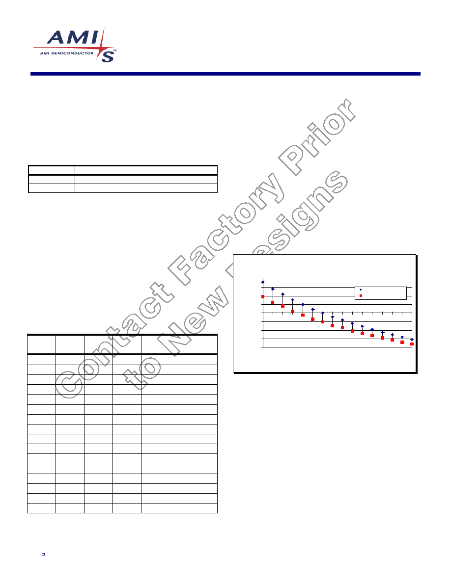
4.7 VCXO
Range
Figure 4 shows the typical effect of the coarse and fine
tuning mechanisms. The difference in VCXO frequency in
parts-per-million (ppm) is shown as the fine tuning volt-
age on the XTUNE pin varies from 0V to 5V. The coarse
tune range as shown is about 350ppm. As the crystal
load capacitance is increased (with increasing Coarse
Tune setting) the frequency is pulled somewhat less with
each coarse step and the fine tuning range decreases.
The fine tuning range always overlaps a few coarse tun-
ing ranges, eliminating the possibility of holes in the
VCXO response. Note that different crystal warping char-
acteristics will change the scaling on the Y-axis, but not
the overall characteristic of the curves.
Figure 4: VCXO Range
VCXO Range (ppm) vs. XTUNE Voltage (V)
-200
-150
-100
-50
0
50
100
150
200
0
1
2
3
4
5
6
7
8
9 10 11 12 13 14 15
Coarse Tune Setting D[11:14]
V
C
X
O
R
ange (ppm)
XTUNE Voltage = 0.0V
XTUNE Voltage = 5.0V