 | –≠–ª–µ–∫—Ç—Ä–æ–Ω–Ω—ã–π –∫–æ–º–ø–æ–Ω–µ–Ω—Ç: FS6108-01 | –°–∫–∞—á–∞—Ç—å:  PDF PDF  ZIP ZIP |
American Microsystems, Inc. reserves the right to change the detail specifications as may be required to permit improvements in the design of its products.
3.4.02
FS6108
FS6108
FS6108
FS6108
-01
-01
-01
-01
1:9 Zero Delay Buffer IC
1:9 Zero Delay Buffer IC
1:9 Zero Delay Buffer IC
1:9 Zero Delay Buffer IC
ISO9001
ISO9001
ISO9001
ISO9001
1.0 Features
∑
Generates up to nine clock outputs, grouped as 4-4-1
from one reference clock input
∑
Pin enable/disable of two banks of four clocks
∑
Auto power-down shuts off PLL, brings outputs low in
the absence of any REF input
∑
Tracking skew < 200ps (spread-spectrum tolerant)
∑
Input-to-output propagation delay < 200ps
∑
Available in a 16-pin 0.150" SOIC
Table 1: Clock Enable Configuration
CONTROL
CLOCK OUTPUTS (MHz)
S2
S1
CLK_A1:4
CLK_B1:4
CLK_FB
Source
0
0
Tristate
Tristate
Driven
PLL
0
1
Driven
Tristate
Driven
PLL
1
0
Driven
Driven
Driven
REF
1
1
Driven
Driven
Driven
PLL
Table 2: Pin Descriptions
Key: DI = Digital Input; DI
U
= Input with Internal Pull-Up; DI
D
= Input with Internal Pull-Down;
DIO = Digital Input/Output; DO = Digital Output; P = Power/Ground; # = Active-low pin
PIN
TYPE
NAME
DESCRIPTION
2
DO
D
CLK_A1
Clock output
3
DO
D
CLK_A2
Clock output
14
DO
D
CLK_A3
Clock output
15
DO
D
CLK_A4
Clock output
Bank A
6
DO
D
CLK_B1
Clock output
7
DO
D
CLK_B2
Clock output
10
DO
D
CLK_B3
Clock output
11
DO
D
CLK_B4
Clock output
Bank B
16
DO
D
CLK_FB
Clock output that also provides an in-
ternal feedback connection to the PLL
1
DI
D
REF
Reference clock input
8, 9
DI
U
S2, S1
Two select inputs that enable and dis-
able the clock outputs, and enable or
bypass the PLL
4, 13
P
VDD
3.3V power supply
5, 12
P
VSS
Ground
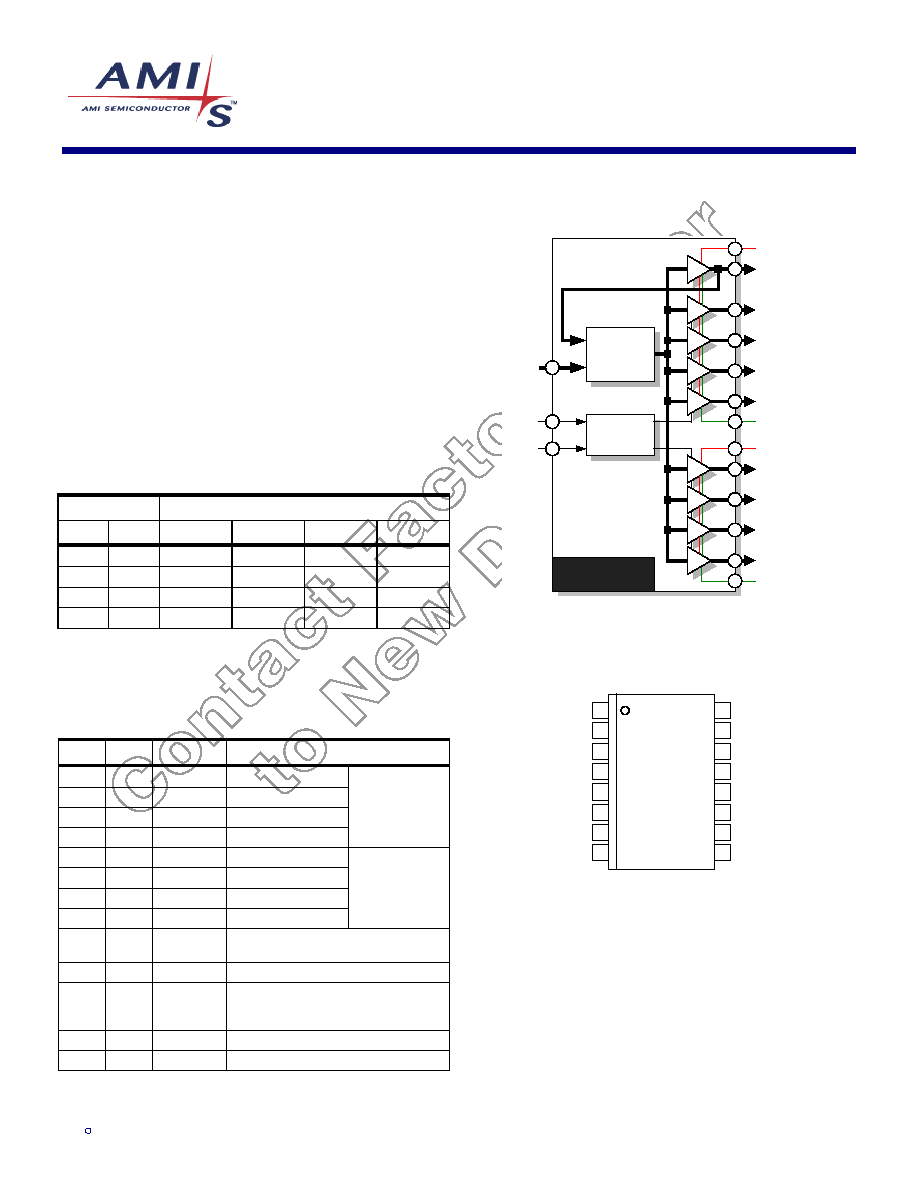
Figure 1: Block Diagram
FS6108
PLL
REF
Control
CLK_B1
VDD
VSS
CLK_B2
CLK_B3
CLK_B4
CLK_A1
VSS
CLK_A2
CLK_A3
CLK_A4
S2
S1
CLK_FB
VDD
Figure 2: Pin Configuration
1
2
3
4
5
6
7
8
CLK_A1
VDD
REF
CLK_B1
CLK_B2
CLK_A4
CLK_A3
VSS
CLK_B3
FS
61
08
CLK_B4
VSS
VDD
S1
9
10
12
11
13
14
16
15
CLK_A2
S2
CLK_FB
3.4.02
2
FS6108
FS6108
FS6108
FS6108
-01
-01
-01
-01
1:9 Zero Delay Buffer IC
1:9 Zero Delay Buffer IC
1:9 Zero Delay Buffer IC
1:9 Zero Delay Buffer IC
ISO9001
ISO9001
ISO9001
ISO9001
2.0 Electrical
Specifications
Table 3: Absolute Maximum Ratings
Stresses above those listed under Absolute Maximum Ratings may cause permanent damage to the device. These conditions represent a stress rating only, and functional operation of the device at
these or any other conditions above the operational limits noted in this specification is not implied. Exposure to maximum rating conditions for extended conditions may affect device performance,
functionality, and reliability.
PARAMETER
SYMBOL
MIN.
MAX.
UNITS
Supply Voltage (V
SS
= ground)
V
DD
V
SS
-0.5
7
V
Input Voltage, dc
V
I
V
SS
-0.5
V
DD
+0.5
V
Output Voltage, dc
V
O
V
SS
-0.5
V
DD
+0.5
V
Input Clamp Current, dc (V
I
< 0 or V
I
> V
DD
)
I
IK
-50
50
mA
Output Clamp Current, dc (V
I
< 0 or V
I
> V
DD
)
I
OK
-50
50
mA
Storage Temperature Range (non-condensing)
T
S
-65
150
∞C
Ambient Temperature Range, Under Bias
T
A
-55
125
∞C
Junction Temperature
T
J
125
∞C
Lead Temperature (soldering, 10s)
260
∞C
Input Static Discharge Voltage Protection (MIL-STD 883E, Method 3015.7)
2
kV
CAUTION: ELECTROSTATIC SENSITIVE DEVICE
Permanent damage resulting in a loss of functionality or performance may occur if this device is subjected to a high-energy elec-
trostatic discharge.
Table 4: Operating Conditions
PARAMETER
SYMBOL
CONDITIONS/DESCRIPTION
MIN.
TYP.
MAX.
UNITS
Supply Voltage
V
DD
3.0
3.3
3.6
V
Operating Temperature Range
T
A
0
70
∞C
Load Capacitance
C
L
CLK_A1:4, CLK_B1:4, CLK_FB
30
pF
Reference Frequency Range
f
REF
10
66.67
MHz
3.4.02
3
FS6108-01
FS6108-01
FS6108-01
FS6108-01
1:9 Zero Delay Buffer IC
1:9 Zero Delay Buffer IC
1:9 Zero Delay Buffer IC
1:9 Zero Delay Buffer IC
ISO9001
ISO9001
ISO9001
ISO9001
Table 5: DC Electrical Specifications
Unless otherwise stated, all power supplies = 3.6V, no load on any output, and ambient temperature range T
A
= 0∞C to 70∞C. Parameters denoted with an asterisk ( * ) represent nominal characteri-
zation data and are not currently production tested to any specific limits. MIN and MAX characterization data are
±
3
from typical. Negative currents indicate current flows out of the device.
PARAMETER
SYMBOL
CONDITIONS/DESCRIPTION
MIN.
TYP.
MAX.
UNITS
Overall
Supply Current, Dynamic,
with Loaded Outputs
I
DD
f
REF
= 66.6MHz; all supplies = 3.465V
36
mA
Supply Current, Static
I
DDs
REF stopped either high or low
20
µ
A
Reference Input (REF)
High-Level Input Voltage
V
IH
2.0
V
DD
+0.3
V
Low-Level Input Voltage
V
IL
V
SS
-0.3
0.8
V
High-Level Input Current (pull-down)
I
IH
V
IH
= 3.3V
25
µ
A
Low-Level Input Current
I
IL
-1
1
µ
A
Digital Inputs (S1, S2)
High-Level Input Voltage
V
IH
2.0
V
DD
+0.3
V
Low-Level Input Voltage
V
IL
V
SS
-0.3
0.8
V
High-Level Input Current
I
IH
-1
1
µ
A
Low-Level Input Current (pull-up)
I
IL
V
IL
= 0V
-30
µ
A
Clock Outputs (CLK_A1:4, CLK_B1:4, CLK_FB)
High Level Output Source Current
I
OH
V
O
= 2.4V
-7
-65
mA
Low Level Output Sink Current
I
OL
V
O
= 0.4V
26
7
mA
z
OL
Measured at 1.5V, output driving low
20
Output Impedance
z
OH
Measured at 1.5V, output driving high
18
Tristate Output Current
I
OZ
-10
10
µ
A
Short Circuit Output Source Current
I
OSH
V
DD
= 3.6V, V
O
= 0V; shorted for 30s, max.
-96
mA
Short Circuit Output Sink Current
I
OSL
V
DD
= V
O
= 3.6V, shorted for 30s, max.
90
mA
Table 6: AC Timing Specifications
Unless otherwise stated, all power supplies = 3.6V, no load on any output, and ambient temperature range T
A
= 25∞C. Parameters denoted with an asterisk ( * ) represent nominal characterization
data and are not currently production tested to any specific limits. MIN and MAX characterization data are
±
3
from typical.
PARAMETER
SYMBOL
CONDITIONS/DESCRIPTION
MIN.
TYP.
MAX.
UNITS
Clock Outputs (CLK_A1:4, CLK_B1:4, CLK_FB)
Duty Cycle *
d
t
Ratio of high pulse width to one clock period,
measured at 1.5V
45
55
%
Jitter, Period (peak-peak) *
t
j(
P)
From rising edge to rising edge at 1.5V, C
L
=30pF
75
ps
Skew, Tracking
t
sk(tr)
±0.5% non-linear (Lexmark) profile @ 31.5kHz
190
ps
Skew, Bank Output-Bank Output
t
sk(b)
CLK_A2 to CLK_B1; C
L
=30pF
250
ps
PLL Reference Zero Delay
t
REF to CLK_FB
150
ps
Rise Time *
t
r
Measured @ 0.8V ≠ 2.0V; C
L
=30pF
1.6
ns
Fall Time *
t
f
Measured @ 2.0V ≠ 0.8V; C
L
=30pF
1.0
ns
3.4.02
4
FS6108
FS6108
FS6108
FS6108
-01
-01
-01
-01
1:9 Zero Delay Buffer IC
1:9 Zero Delay Buffer IC
1:9 Zero Delay Buffer IC
1:9 Zero Delay Buffer IC
ISO9001
ISO9001
ISO9001
ISO9001
3.0 Package
Information
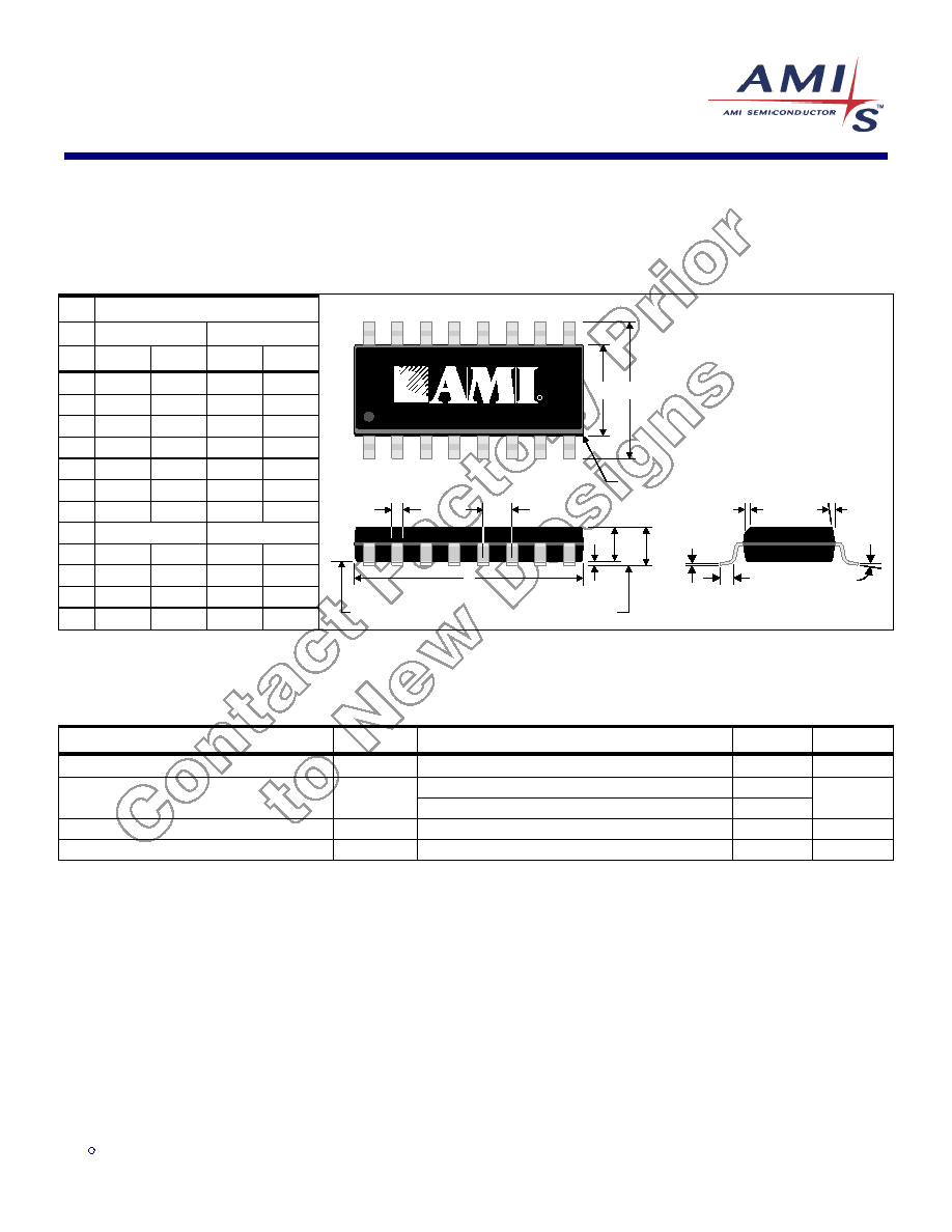
Table 7: 16-pin SOIC (0.150") Package Dimensions
DIMENSIONS
INCHES
MILLIMETERS
MIN.
MAX.
MIN.
MAX.
A
0.061
0.068
1.55
1.73
A1
0.004
0.0098
0.102
0.249
A2
0.055
0.061
1.40
1.55
B
0.013
0.019
0.33
0.49
C
0.0075
0.0098
0.191
0.249
D
0.386
0.393
9.80
9.98
E
0.150
0.157
3.81
3.99
e
0.050 BSC
1.27 BSC
H
0.230
0.244
5.84
6.20
h
0.010
0.016
0.25
0.41
L
0.016
0.035
0.41
0.89
0
∞
8
∞
0
∞
8
∞
B
e
D
A
1
SEATING PLANE
H
E
16
1
ALL RADII:
0.005" TO 0.01"
BASE PLANE
A
2
C
L
7∞ typ.
h x 45∞
A
AMERICAN MICROSYSTEMS, INC.
R
Table 8: 16-pin SOIC (0.150") Package Characteristics
PARAMETER
SYMBOL
CONDITIONS/DESCRIPTION
TYP.
UNITS
Thermal Impedance, Junction to Free-Air
JA
Air flow = 0 m/s
109
∞C/W
Corner lead
4.0
Lead Inductance, Self
L
11
Center lead
3.0
nH
Lead Inductance, Mutual
L
12
Any lead to any adjacent lead
0.4
nH
Lead Capacitance, Bulk
C
11
Any lead to V
SS
0.5
pF

3.4.02
5
FS6108-01
FS6108-01
FS6108-01
FS6108-01
1:9 Zero Delay Buffer IC
1:9 Zero Delay Buffer IC
1:9 Zero Delay Buffer IC
1:9 Zero Delay Buffer IC
ISO9001
ISO9001
ISO9001
ISO9001
4.0 Ordering
Information
Table 9: Device Ordering Codes
DEVICE NUMBER
ORDERING CODE
PACKAGE TYPE
OPERATING
TEMPERATURE RANGE
SHIPPING
CONFIGURATION
12055-801
16-pin (0.150") SOIC
0
∞
C to 70
∞
C (Commercial)
Tape and Reel
FS6108-01
12055-801
16-pin (0.150") SOIC
0
∞
C to 70
∞
C (Commercial)
Tubes
Copyright © 2000 American Microsystems, Inc.
Devices sold by AMI are covered by the warranty and patent indemnification provisions appearing in its Terms of Sale only. AMI
makes no warranty, express, statutory implied or by description, regarding the information set forth herein or regarding the freedom
of the described devices from patent infringement. AMI makes no warranty of merchantability or fitness for any purposes. AMI re-
serves the right to discontinue production and change specifications and prices at any time and without notice. AMI's products are
intended for use in commercial applications. Applications requiring extended temperature range, unusual environmental require-
ments, or high reliability applications, such as military, medical life-support or life-sustaining equipment, are specifically not recom-
mended without additional processing by AMI for such applications.
American Microsystems, Inc., 2300 Buckskin Rd., Pocatello, ID 83201, (208) 233-4690, FAX (208) 234-6796,
WWW Address:
http://www.amis.com
E-mail:
tgp@amis.com