
American Microsystems, Inc. reserves the right to change the detail specifications as may be required to permit improvements in the design of its products.
ISO9001
ISO9001
ISO9001
ISO9001
QS9000
QS9000
QS9000
QS9000
FS612510-01/-02
FS612510-01/-02
FS612510-01/-02
FS612510-01/-02
1:10 Zero-Delay Clock Buffer IC
1:10 Zero-Delay Clock Buffer IC
1:10 Zero-Delay Clock Buffer IC
1:10 Zero-Delay Clock Buffer IC
1.0 Features
�
Generates one bank of ten clock outputs (1Y0 to
1Y9) from one reference clock input (CLK)
�
Designed to meet the PLL Component Specifications
as noted in the PC133 SDRAM Registered DIMM
Design Specification
�
External feedback input (FBIN) to synchronize all
clock outputs to the reference input
�
Operating frequency 25MHz to 140MHz
�
Tight tracking skew (spread-spectrum tolerant)
�
On-chip
25
series damping resistors for driving
point-to-point loads
�
Output enable (G) enables or disables low all clock
outputs
�
Available with an auto power-down option that turns
off the PLL and forces all outputs low when the refer-
ence clock stops (FS612510-02)
�
Packaged in a 24-pin TSSOP
Figure 1: Block Diagram
FS612510
1Y0
1Y1
1Y2
1Y3
1Y4
1Y5
1Y6
1Y7
1Y8
PLL
FBIN
CLK
G
FBOUT
AVDD
1Y9
VDD
GND
AGND
2.0 Description
The FS612510 is a low skew, low jitter CMOS zero-delay
phase-lock loop (PLL) clock buffer IC designed for high-
speed motherboard applications, such as those using
133MHz SDRAM.
Ten buffered clock outputs are derived from an onboard
open-loop PLL. The PLL aligns the frequency and phase
of all output clocks to the reference input clock CLK, in-
cluding an FBOUT clock that feeds back to FBIN to close
the loop. Multiple power and ground supplies help reduce
the effects of noise on device performance.
All ten outputs 1Y0 to 1Y9 are enabled and disabled low
by the active-high G signal. The PLL can be bypassed for
test purposes by pulling AVDD to ground.
Figure 2: Pin Configuration
1
2
3
4
5
6
7
8
24
23
22
21
20
19
AGND
VDD
1Y0
AVDD
CLK
9
10
11
12
GND
GND
1Y3
1Y4
VDD
G
FBOUT
18
17
16
15
14
13
1Y6
GND
1Y7
GND
1Y8
1Y5
VDD
FBIN
FS612510
1Y1
1Y2
VDD
1Y9
Table 1: Function Table
INPUT
OUTPUT
PLL
AVDD
G
CLK
1Y0-1Y9
FBOUT
H
L
L
L
L
H
L
H
L
H
H
H
L
L
L
Z
e
ro-Del
ay
H
H
H
H
H
L
L
L
L
L
L
L
H
L
H
L
H
L
L
L
P
LL B
y
pa
s
s
L
H
H
H
H
ISO9001
ISO9001
ISO9001
ISO9001
QS9000
QS9000
QS9000
QS9000
2
FS612510-01/-02
FS612510-01/-02
FS612510-01/-02
FS612510-01/-02
1:10 Zero-Delay Clock Buffer IC
1:10 Zero-Delay Clock Buffer IC
1:10 Zero-Delay Clock Buffer IC
1:10 Zero-Delay Clock Buffer IC
Table 2: Pin Descriptions
Key: AI = Analog Input; AO = Analog Output; DI = Digital Input; DI
U
= Input with Internal Pull-Up; DI
D
= Input with Internal Pull-Down; DIO = Digital Input/Output; DI-3 = Three-Level Digital Input,
DO = Digital Output; P = Power/Ground; # = Active Low pin
PIN
TYPE
NAME
DESCRIPTION
3
DO
1Y0
Clock output
4
DO
1Y1
Clock output
5
DO
1Y2
Clock output
8
DO
1Y3
Clock output
9
DO
1Y4
Clock output
15
DO
1Y5
Clock output
16
DO
1Y6
Clock output
17
DO
1Y7
Clock output
20
DO
1Y8
Clock output
21
DO
1Y9
Clock output
Enabled by G
23
P
AVDD
Power Supply / Test mode enable. This pin provides the power supply to the internal PLL. When the
pin is pulled low, the PLL is bypassed and the output clocks directly follow the input clock
1
P
AGND
PLL supply ground
24
DI
CLK
Reference clock input (Note: -02 version has a pull-down on this pin)
13
DI
FBIN
Feedback clock input; must be connected to FBOUT to complete the loop
12
DO
FBOUT
Feedback output clock
11
DI
G
Output enable stops all clocks (1Y0 � 1Y9) in a low state when this pin is low
6, 7, 18, 19
P
GND
Ground for all clock outputs
2, 10, 14, 22
P
VDD
Power supply for all clock outputs

ISO9001
ISO9001
ISO9001
ISO9001
QS9000
QS9000
QS9000
QS9000
3
FS612510-01/-02
FS612510-01/-02
FS612510-01/-02
FS612510-01/-02
1:10 Zero-Delay Clock Buffer IC
1:10 Zero-Delay Clock Buffer IC
1:10 Zero-Delay Clock Buffer IC
1:10 Zero-Delay Clock Buffer IC
3.0 Device
Operation
The FS612510 is a zero-delay buffer intended for use on
buffered PC133 SDRAM DIMMs.
The FS612510 precisely aligns the frequency and phase
of the output clocks to the input CLK by use of an on-chip
phase-lock loop (PLL). The PLL generates up to 10 low-
skew, low-jitter copies of the CLK, with the outputs ad-
justed for 50% duty cycle.
The FBOUT clock must be hardwired to the FBIN pin to
complete the loop. The PLL actively adjusts the output
clocks so that there is no phase error between the refer-
ence clock (CLK) and the feedback clock (FBIN).
Since the device uses a PLL to lock the output clocks to
the input clock, there is a power-up stabilization time that
is required for the PLL to achieve phase lock.
Note that all inputs and outputs use LVCMOS signal lev-
els.
3.1 PLL
Bypass
When the AVDD pin is pulled low, the reference clock
signal bypasses the PLL and is muxed directly through to
the outputs. The PLL is powered down, and device acts a
fanout buffer.
Note that if AVDD is re-established, the PLL requires a
power-up and stabilization time to lock to the input clock.
3.2 Output
Enable/Disable
All ten outputs are enabled or disabled as a group by the
G enable signal.
A logic-high on G input enables all the clock outputs to
swing in phase with the reference clock. A logic-low on G
forces all of the clock outputs to a logic-low state.
The function table Table 1 shows the effect of the G en-
able signal on the clock outputs.
3.3 Power-Down
The FS612510-02 version provides an auto power-down
feature that shuts off the PLL, drives all outputs low, and
places the device into a low current state if the reference
clock stops. The power-down circuit is level sensitive,
and detects either a DC high or low on the CLK input.
4.0 Tracking
Skew
PLL-based buffer ICs may be required to follow a spread-
spectrum modulated reference clock for frequencies
greater than 66MHz. Spread spectrum modulation limits
peak EMI emissions by intentionally introducing jitter onto
a clock signal, effectively spreading the peak energy over
a range of frequencies.
A downstream PLL, contained in a clock buffer IC such
as this one, must carefully track the modulated input ref-
erence clock. A measure of how closely the downstream
PLL follows the modulated clock is called the tracking
skew. To ensure a tight tracking skew, the loop band-
width of a downstream PLL is increased and the loop
phase angle is reduced over that of typical PLL-based
clock generators.
The type of modulation profile used impacts tracking
skew. The maximum frequency change occurs at the
profile limits where the modulation changes the slew rate
polarity. To track the sudden reversal in clock frequency,
the downstream PLL must have a large loop bandwidth.
The ability of the downstream PLL to catch up to the
modulating clock is determined by the loop transfer func-
tion phase angle.
The spread-spectrum reference clock should be either a
triangle-wave or a non-linear (Lexmark) modulation pro-
file, with a modulation frequency of 50kHz or less.
ISO9001
ISO9001
ISO9001
ISO9001
QS9000
QS9000
QS9000
QS9000
4
FS612510-01/-02
FS612510-01/-02
FS612510-01/-02
FS612510-01/-02
1:10 Zero-Delay Clock Buffer IC
1:10 Zero-Delay Clock Buffer IC
1:10 Zero-Delay Clock Buffer IC
1:10 Zero-Delay Clock Buffer IC
5.0 Electrical
Specifications
Table 3: Absolute Maximum Ratings
Stresses above those listed under Absolute Maximum Ratings may cause permanent damage to the device. These conditions represent a stress rating only, and functional operation of the device at
these or any other conditions above the operational limits noted in this specification is not implied. Exposure to maximum rating conditions for extended conditions may affect device performance,
functionality, and reliability.
PARAMETER
SYMBOL
MIN.
MAX.
UNITS
Supply Voltage, dc, Clock Buffers (V
SS
= ground)
AV
DD
V
SS
- 0.5
7
V
Supply Voltage, dc, Core
V
DD
V
SS
- 0.5
7
V
Input Voltage, dc
V
I
V
SS
- 0.5
V
DD
+0.5
V
Output Voltage, dc
V
O
V
SS
- 0.5
V
DD
+0.5
V
Input Clamp Current, dc (V
I
< 0 or V
I
> V
DD
)
I
IK
-50
50
mA
Output Clamp Current, dc (V
I
< 0 or V
I
> V
DD
)
I
OK
-50
50
mA
Storage Temperature Range (non-condensing)
T
S
-65
150
�C
Ambient Temperature Range, Under Bias
T
A
-55
125
�C
Junction Temperature
T
J
125
�C
Lead Temperature (soldering, 10s)
260
�C
Static Discharge Voltage Protection (MIL-STD 883E, Method 3015.7)
2
kV
CAUTION: ELECTROSTATIC SENSITIVE DEVICE
Permanent damage resulting in a loss of functionality or performance may occur if this device is subjected to a high-energy
electrostatic discharge.
Table 4: Operating Conditions
PARAMETER
SYMBOL
CONDITIONS/DESCRIPTION
MIN.
TYP.
MAX.
UNITS
Supply Voltage, Core and Outputs
V
DD
3.3V � 10%
3.0
3.3
3.6
V
Ambient Operating Temperature Range
T
A
0
70
�C
Output Load Capacitance
C
L
15
pF
Input Frequency
f
CLK
CLK
50
140
MHz
Input Duty Cycle
CLK
40
60
%
Input Rise/Fall Time
CLK
3
ns
ISO9001
ISO9001
ISO9001
ISO9001
QS9000
QS9000
QS9000
QS9000
5
FS612510-01/-02
FS612510-01/-02
FS612510-01/-02
FS612510-01/-02
1:10 Zero-Delay Clock Buffer IC
1:10 Zero-Delay Clock Buffer IC
1:10 Zero-Delay Clock Buffer IC
1:10 Zero-Delay Clock Buffer IC
Table 5: DC Electrical Specifications
Unless otherwise stated, all power supplies = 3.3V%, no load on any output, and ambient temperature range T
A
= 0�C to 70�C. Parameters denoted with an asterisk ( * ) represent nominal charac-
terization data and are not currently production tested to any specific limits. MIN and MAX characterization data are
�
3
from typical. Negative currents indicate current flows out of the device.
PARAMETER
SYMBOL
CONDITIONS/DESCRIPTION
MIN.
TYP.
MAX.
UNITS
Overall
Supply Current, Dynamic
f
CLK
= 133.33MHz; V
DD
= 3.3V
135
mA
Supply Current, Static
I
DDL
Outputs low; V
DD
= 3.3V
3
mA
Output Enable Input (G)
High-Level Input Voltage
V
IH
2.0
V
DD
+0.3
V
Low-Level Input Voltage
V
IL
V
SS
-0.3
0.8
V
Input Leakage Current
I
I
-5
5
�
A
Clock Inputs (CLK, FBIN)
High-Level Input Voltage
V
IH
2.0
V
DD
+0.3
V
Low-Level Input Voltage
V
IL
V
SS
-0.3
0.8
V
-01 version
-5
5
Input Leakage Current
I
I
-02 version has a pull-down on CLK
28
�
A
Input Loading Capacitance *
C
L(in)
As seen by an external clock driver
4
pF
Clock Outputs (1Y0:9, FBOUT)
V
DD
= 2.9V, V
O
= 2.0V
-18
-12
High-Level Output Source Current
I
OH
V
DD
= 3.7V, V
O
= 2.0V
-35
-12
mA
V
DD
= 2.9V, V
O
= 0.8V
12
16
Low-Level Output Sink Current
I
OL
V
DD
= 3.7V, V
O
= 0.8V
12
17
mA
Output Impedance
z
O
33
Tristate Output Current
I
OZ
-10
10
�
A
Short Circuit Source Current *
I
OSH
V
O
= 0V; shorted for 30s, max.
-60
mA
Short Circuit Sink Current *
I
OSL
V
O
= 3.3V; shorted for 30s, max.
90
mA
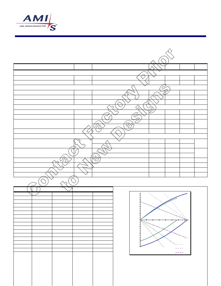
Table 6: Clock Output Drive (1Y0:4, 2Y0:3, FBOUT)
Voltage
Low Drive Current (mA)
High Drive Current (mA)
0.1 V
-47
-59
2
2
0.2 V
-45
-58
4
4
0.4 V
-43
-56
8
9
0.6 V
-40
-55
12
13
0.8 V
-38
-52
16
17
1.0 V
-35
-50
20
21
1.2 V
-32
-47
24
25
1.4 V
-29
-45
27
29
1.6 V
-26
-41
31
33
1.8 V
-22
-38
34
36
2.0 V
-18
-35
38
40
2.2 V
-15
-31
41
43
2.4 V
-10
-28
43
46
2.6 V
-6
-24
45
49
2.8 V
-2
-20
48
51
3.0 V
0
-15
49
53
3.3 V
-9
56
-60
-45
-30
-15
0
15
30
45
60
0
0.5
1
1.5
2
2.5
3
3.5
Output Voltage (V)
Out
put
Cur
r
e
nt
(
m
A)
30
50
90