 | –≠–ª–µ–∫—Ç—Ä–æ–Ω–Ω—ã–π –∫–æ–º–ø–æ–Ω–µ–Ω—Ç: FS6205 | –°–∫–∞—á–∞—Ç—å:  PDF PDF  ZIP ZIP |
American Microsystems, Inc. reserves the right to change the detail specifications as may be required to permit improvements in the design of its products.
2.28.02
FS6205
FS6205
FS6205
FS6205
VCXO Clock Generator IC
VCXO Clock Generator IC
VCXO Clock Generator IC
VCXO Clock Generator IC
ISO9001
ISO9001
ISO9001
ISO9001
1.0 Features
∑
On-chip tunable voltage-controlled crystal oscillator
circuitry (VCXO) allows precise system frequency
tuning (pull range typically 300ppm)
∑
Uses inexpensive fundamental-mode crystals
∑
Integrated phase-locked loops (PLL) multiply VCXO
frequency to the higher system frequencies needed
∑
3.3V supply voltage available (contact factory for 5
volt versions)
∑
Small circuit board footprint (8-pin 0.150
SOIC)
∑
Custom frequency selections available - contact your
local AMI Sales Representative for more information
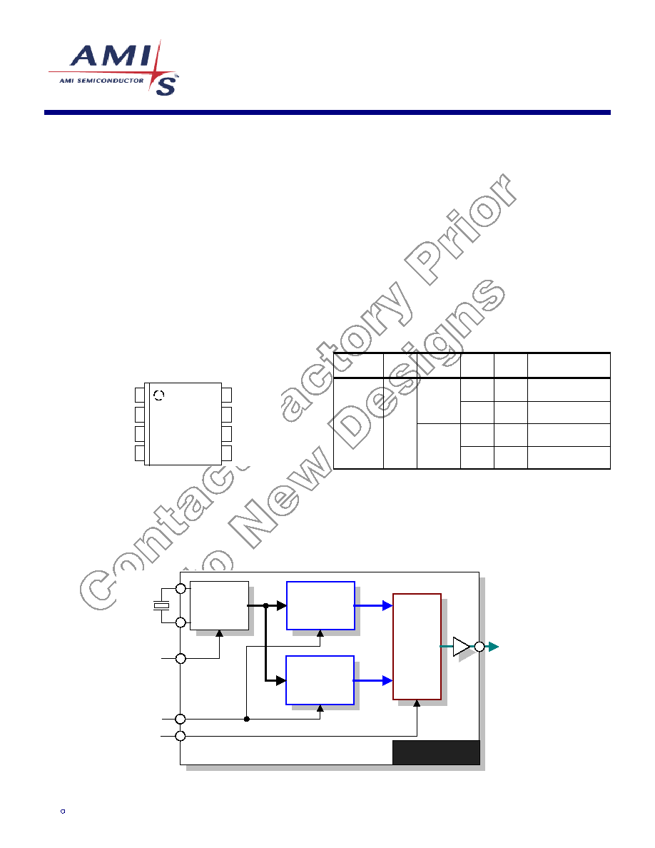
Figure 1: Pin Configuration
1
8
2
3
4
7
6
5
XIN
VDD
XTUNE
VSS
MS
FS
CLK
XOUT
FS6
205
8-pin (0.150
) SOIC
2.0 Description
The FS6205 is a monolithic CMOS clock generator IC
designed to minimize cost and component count in digital
video/audio systems.
An on-chip voltage-controlled crystal oscillator (VCXO)
permits the reference frequency (or output frequency) to
be tuned to match other frequencies present in the sys-
tem.
Phase-locked loops are used to generate precise output /
reference frequency ratios. See Table 1 for information
on the frequency ratios programmed into each version of
the FS6205.
Table 1: Version Information
DEVICE
VDD
(nom)
F
REF
(MHz)
FS
MS
CLK
(MHz)
0
0
27.000
(REF * 2)
13.500
0
1
74.175824175...
(REF * 500 / 91)
1
0
27.027
(REF * 2)
FS6205-01
3.3
13.5135
1
1
74.580835443...
(REF * 436 / 79)
NOTE: Contact AMI for custom versions
Figure 2: Block Diagram
VCXO
FS6205
CLK
PLL A
XOUT
XIN
XTUNE
MUX
FS
MS
PLL B

2
2.28.02
FS6205
FS6205
FS6205
FS6205
VCXO
VCXO
VCXO
VCXO Clock Generator IC
Clock Generator IC
Clock Generator IC
Clock Generator IC
ISO9001
ISO9001
ISO9001
ISO9001
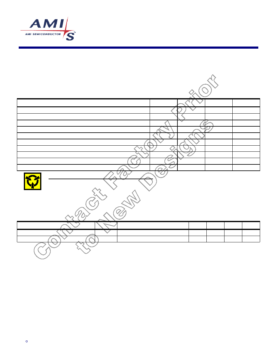
Table 2: Pin Descriptions
Key: AI = Analog Input; AO = Analog Output; DI = Digital Input; DI
U
= Input with Internal Pull-Up; DI
D
= Input with Internal Pull-Down; DIO = Digital Input/Output; DI-3 = Three-Level Digital Input,
DO = Digital Output; P = Power/Ground; # = Active Low pin
PIN
TYPE
NAME
DESCRIPTION
1
AI
XIN
VCXO Crystal Feedback
2
P
VDD
Power Supply (+3.3V nominal)
3
AI
XTUNE
VCXO Tune
4
P
VSS
Ground
5
DO
CLK
Clock Output
6
DI
U
FS
Frequency Select Input (changes PLL Frequencies)
7
DI
U
MS
Multiplexer Select Input (chooses PLL A or PLL B)
8
AO
XOUT
VCXO Crystal Drive
3.0 Functional Block Description
3.1
Phase-Locked Loops (PLL)
The on-chip PLLs are a standard frequency- and phase-
locked loop architecture. The PLL multiplies the reference
oscillator to the desired frequency by a ratio of integers.
The frequency multiplication is exactly that specified by
the integer ratios.
3.2 Voltage-Controlled
Crystal
Oscillator (VCXO)
The VCXO provides a tunable, low-jitter frequency refer-
ence for the rest of the FS6205 system components.
Loading capacitance for the crystal is internal to the
FS6205. No external components (other than the crystal
resonator itself) are required for operation of the VCXO.
Continuous fine-tuning of the VCXO frequency is accom-
plished by varying the voltage on the XTUNE pin. The
total change (from one extreme to the other) in effective
loading capacitance is 12pF nominal (i.e from 35pF to
13pF).
"Pulling" of the crystal oscillation frequency, is accom-
plished by altering the effective load capacitance pre-
sented to the crystal by the oscillator circuit. The actual
amount that changing the load capacitance alters the os-
cillator frequency will be dependent on the characteristics
of the crystal as well as the oscillator circuit itself.
Specifically, the motional capacitance of the crystal (usu-
ally referred to by crystal manufacturers as C
1
), the static
capacitance of the crystal (C
0
), and the load capacitance
(C
L
) of the oscillator determine the "warping" or "pulling"
capability of the crystal in the oscillator circuit.
A simple formula to obtain the pulling capability of a
crystal oscillator is:
(
)
(
) (
)
C
C
C
C
C
C
C
ppm
f
L
L
L
L
1
0
2
0
6
1
2
1
2
10
)
(
+
◊
+
◊
◊
-
◊
=
where C
L1
and C
L2
are the two extremes of the applied
load capacitance.
EXAMPLE: A crystal with the following parameters is
used. With C
1
= 0.02pF, C
0
= 5pF, C
L1
= 13pF, and C
L2
=
35pF, the tuning range between extreme settings of
XTUNE voltage is:
(
)
(
) (
)
ppm
.
f
306
13
5
35
5
2
106
13
35
02
0
+
◊
+
◊
◊
-
◊
=
.
-250
-200
-150
-100
-50
0
50
100
150
200
250
0
0.5
1
1.5
2
2.5
3
3.5
V(XTUNE) - volts
D
e
v
i
a
t
ion -
ppm
Figure 3 - Typical VCXO Characteristic
3
2.28.02
FS6205
FS6205
FS6205
FS6205
VCXO Clock Generator IC
VCXO Clock Generator IC
VCXO Clock Generator IC
VCXO Clock Generator IC
ISO9001
ISO9001
ISO9001
ISO9001
4.0 Electrical
Specifications
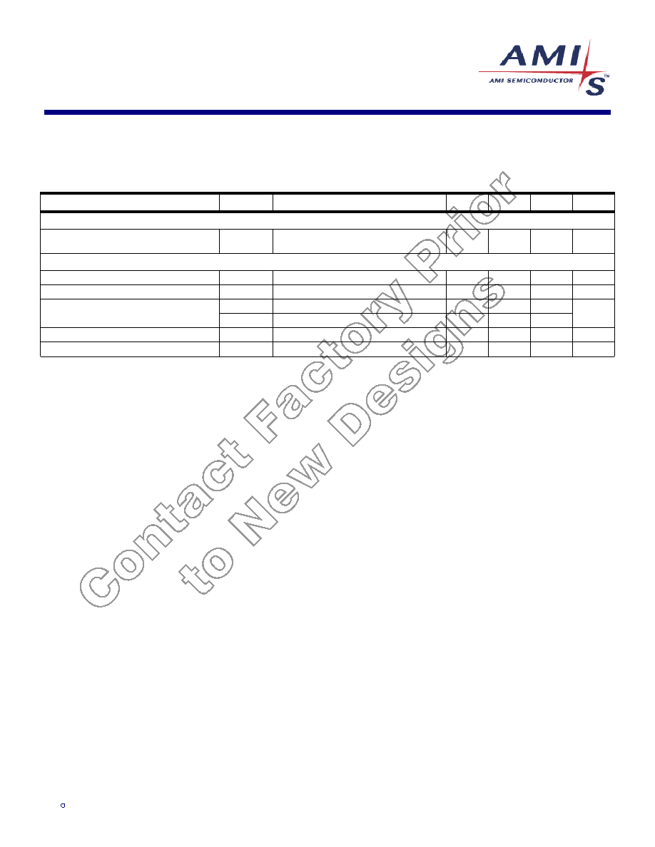
Table 3: Absolute Maximum Ratings
Stresses above those listed under Absolute Maximum Ratings may cause permanent damage to the device. These conditions represent a stress rating only, and functional operation of the device at
these or any other conditions above the operational limits noted in this specification is not implied. Exposure to maximum rating conditions for extended conditions may affect device performance,
functionality, and reliability.
PARAMETER
SYMBOL
MIN.
MAX.
UNITS
Supply Voltage (V
SS
= ground)
V
DD
V
SS
-0.5
7
V
Input Voltage, dc
V
I
V
SS
-0.5
V
DD
+0.5
V
Output Voltage, dc
V
O
V
SS
-0.5
V
DD
+0.5
V
Input Clamp Current, dc (V
I
< 0 or V
I
> V
DD
)
I
IK
-50
50
mA
Output Clamp Current, dc (V
I
< 0 or V
I
> V
DD
)
I
OK
-50
50
mA
Storage Temperature Range (non-condensing)
T
S
-65
150
∞C
Ambient Temperature Range, Under Bias
T
A
-55
125
∞C
Junction Temperature
T
J
125
∞C
Lead Temperature (soldering, 10s)
260
∞C
Input Static Discharge Voltage Protection (MIL-STD 883E, Method 3015.7)
2
kV
CAUTION: ELECTROSTATIC SENSITIVE DEVICE
Permanent damage resulting in a loss of functionality or performance may occur if this device is subjected to a high-energy elec-
trostatic discharge.
Table 4: Operating Conditions
PARAMETER
SYMBOL
CONDITIONS/DESCRIPTION
MIN.
TYP.
MAX.
UNITS
Supply Voltage (3.3 volt system)
V
DD
3.0
3.3
3.6
V
Ambient Operating Temperature Range
T
A
0
70
∞C
4
2.28.02
FS6205
FS6205
FS6205
FS6205
VCXO
VCXO
VCXO
VCXO Clock Generator IC
Clock Generator IC
Clock Generator IC
Clock Generator IC
ISO9001
ISO9001
ISO9001
ISO9001
Table 5: DC Electrical Specifications
Unless otherwise stated, V
DD
= 3.3V ± 10%, no load on any output, and ambient temperature range T
A
= 0∞C to 70∞C. Parameters denoted with an asterisk ( * ) represent nominal characterization
data and are not production tested to any specific limits. Where given, MIN and MAX characterization data are
±
3
from typical. Negative currents indicate current flows out of the device.
PARAMETER
SYMBOL
CONDITIONS/DESCRIPTION
MIN.
TYP.
MAX.
UNITS
Overall
Supply Current, Dynamic, with Loaded
Outputs
I
DD
f
XTAL
= 13.5MHz; C
L
= 10pF, V
DD
= 3.3V
12
mA
Clock Outputs (CLKx)
High-Level Output Source Current *
I
OH
V
O
= 2.0V
-40
mA
Low-Level Output Sink Current *
I
OL
V
O
= 0.4V
17
mA
z
OH
V
O
= 0.5V
DD
; output driving high
25
Output Impedance *
z
OL
V
O
= 0.5V
DD
; output driving low
25
Short Circuit Source Current *
I
OSH
V
O
= 0V; shorted for 30s, max.
-55
mA
Short Circuit Sink Current *
I
OSL
V
O
= 3.3V; shorted for 30s, max.
55
mA

5
2.28.02
FS6205
FS6205
FS6205
FS6205
VCXO Clock Generator IC
VCXO Clock Generator IC
VCXO Clock Generator IC
VCXO Clock Generator IC
ISO9001
ISO9001
ISO9001
ISO9001
Table 6: AC Timing Specifications
Unless otherwise stated, V
DD
= 3.3V ± 10%, no load on any output, and ambient temperature range T
A
= 0∞C to 70∞C. Parameters denoted with an asterisk ( * ) represent nominal characterization
data and are not production tested to any specific limits. Where given, MIN and MAX characterization data are
±
3
from typical.
PARAMETER
SYMBOL
CONDITIONS/DESCRIPTION
MIN.
TYP.
MAX.
UNITS
Overall
Synthesis Error
(unless otherwise noted in Frequency Table)
0
ppm
Crystal Oscillator
Center Frequency Tuning Volt-
age
V
CENTER
For crystal with specified C
L(xtal)
1.4
V
Center Frequency Crystal
Loading Capacitance
C
L(xtal)
As seen by a crystal connected to XIN and XOUT
(@V
XTUNE
=V
CENTER
). Crystal loading capacitance at
nominal center frequency should be specified for this
value.
20
pF
Crystal Drive Level
R
XTAL
=20
;
200
uW
Clock Output (CLK)
Duty Cycle *
Ratio of high pulse width (as measured from rising edge to next falling
edge at V
DD
/2) to one clock period
45
55
%
Jitter, Period (peak-peak) *
t
j(
P)
From rising edge to next rising edge at V
DD
/2
150
ps
Jitter, Long Term (
y
(
)) *
t
j(LT)
From 0-500
µ
s at V
DD
/2 compared to ideal clock
source (CLK =27MHz or 27.027MHz)
65
ps
Jitter, Long Term (
y
(
)) *
t
j(LT)
From 0-500
µ
s at V
DD
/2 compared to ideal clock
source (CLK = 74.175MHz or 74.58MHz)
200
ps
Rise Time *
t
r
V
DD
= 3.3V; V
O
= 0.3V to 3.0V; C
L
= 10pF
1.2
ns
Fall Time *
t
f
V
DD
= 3.3V; V
O
= 3.0V to 0.3V; C
L
= 10pF
1.2
ns