 | –≠–ª–µ–∫—Ç—Ä–æ–Ω–Ω—ã–π –∫–æ–º–ø–æ–Ω–µ–Ω—Ç: FS6322-03 | –°–∫–∞—á–∞—Ç—å:  PDF PDF  ZIP ZIP |

This document contains information on a product under development. American Microsystems, Inc. reserves the right to change or discontinue this product without notice.
3.1.02
FS6322-03
FS6322-03
FS6322-03
FS6322-03
Three-PLL Clock Generator IC
Three-PLL Clock Generator IC
Three-PLL Clock Generator IC
Three-PLL Clock Generator IC
ISO9001
ISO9001
ISO9001
ISO9001
1.0 Features
∑
Three PLLs with deep reference, feedback, and post
dividers to provide precision clock frequencies
∑
Multiple outputs provide several clocking options
∑
Outputs may be tristated for board testing
∑
S0, S1, and S2 inputs modify output frequencies for
design flexibility
∑
3.3V
operation
∑
Accepts 5 to 30MHz crystals
∑
Custom frequency patterns, pinouts, and packages
are available. Contact your local AMI Sales Repre-
sentative for more information.
2.0 Description
The FS6322 is a ROM-based CMOS clock generator IC
designed to minimize cost and component count in a va-
riety of electronic systems.
Three low-jitter phase-locked loops (PLLs) drive up to five
low-skew clock outputs to provide a high degree of flexi-
bility. The device is packaged in a 16-pin SOIC to mini-
mize board space.
High-resolution divider capability permits generation of
desired frequencies.
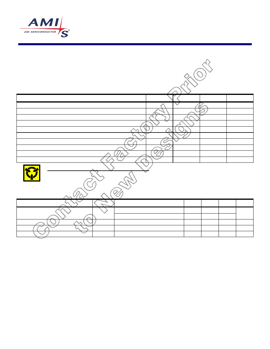
Figure 1: Pin Configuration
1
16
2
3
4
5
6
7
8
15
14
13
12
11
10
9
CLK_C
VDD
VSS
XIN
XOUT
CLK_E
CLK_D
CLK_F
CLK_B
CLK_A
VSS
S0
S1
VDD
S2
OE
F
S
63
22
16-pin (0.150") SOIC
Figure 2: Block Diagram
FS6322-03
Crystal
Oscillator
XOUT
XIN
PLL A
PLL B
PLL C
Clock
Logic
CLK_E
CLK_F
CLK_A
CLK_B
CLK_C
CLK_D
S2:S0
OE
Device
Control

2
3.1.02
FS6322-03
FS6322-03
FS6322-03
FS6322-03
Three-PLL Clock Generator IC
Three-PLL Clock Generator IC
Three-PLL Clock Generator IC
Three-PLL Clock Generator IC
Table 1: Pin Descriptions
Key: AI = Analog Input; AO = Analog Output; DI = Digital Input; DI
U
= Input with Internal Pull-Up; DI
D
= Input with Internal Pull-Down; DIO = Digital Input/Output; DI-3 = Three-Level Digital Input,
DO = Digital Output; P = Power/Ground; # = Active Low pin
PIN
TYPE
NAME
DESCRIPTION
1
DO
CLK_C
C clock output
2
P
VDD
Power supply (5V to 3.3V)
3
P
VSS
Ground
4
AI
XIN
Crystal oscillator feedback
5
AO
XOUT
Crystal oscillator drive
6
DO
CLK_E
E clock output
7
DO
CLK_D
D clock output
8
DO
CLK_F
F clock output
9
DO
CLK_B
A clock output
10
DO
CLK_A
B clock output
11
P
VSS
Ground
12
DI
S0
Frequency select control input
13
DI
S1
Frequency select control input
14
P
VDD
Power supply (5V to 3.3V)
15
DI
S2
Frequency select control input
16
DI
OE
Output enable input: logic-high enables outputs; logic-low tristates outputs (high impedance)
Table 2: Frequency Table ≠ FS6322-03 (3.3volt)
S2
S1
S0
FREF
CLK_A
(pin 10)
CLK_B
(pin 9)
CLK_C
(pin 1)
CLK_D
(pin 7)
CLK_E
(pin 6)
CLK_F
(pin 8)
0
0
0
14.919
OFF
48.00026
OFF
24.61635
14.91900
OFF
0
0
1
14.31818
14.31818
8.00000
66.00000
20.00000
24.57598
48.00000
0
1
0
11.0592
27.00000
16.93440
22.57920
33.86880
22.57920
33.86880
0
1
1
11.0592
27.00000
22.57920
33.86880
45.15840
33.86880
33.86880
1
0
0
14.919
OFF
48.00026
29.49105
24.61635
14.91900
OFF
1
0
1
14.31818
14.31818
8.00000
83.00071
20.00000
24.57598
48.00000
1
1
0
11.0592
27.00000
18.43200
24.57600
36.86400
24.57600
33.86880
1
1
1
11.0592
27.00000
24.57600
36.86400
49.15200
36.86400
33.86880
3
3.1.02
FS6322-03
FS6322-03
FS6322-03
FS6322-03
Three-PLL Clock Generator IC
Three-PLL Clock Generator IC
Three-PLL Clock Generator IC
Three-PLL Clock Generator IC
3.0 Electrical
Specifications
Table 3: Absolute Maximum Ratings
Stresses above those listed under Absolute Maximum Ratings may cause permanent damage to the device. These conditions represent a stress rating only, and functional operation of the device at
these or any other conditions above the operational limits noted in this specification is not implied. Exposure to maximum rating conditions for extended conditions may affect device performance,
functionality, and reliability.
PARAMETER
SYMBOL
MIN.
MAX.
UNITS
Supply Voltage, dc (V
SS
= ground)
V
DD
V
SS
-0.5
7
V
Input Voltage, dc
V
I
V
SS
-0.5
V
DD
+0.5
V
Output Voltage, dc
V
O
V
SS
-0.5
V
DD
+0.5
V
Input Clamp Current, dc (V
I
< 0 or V
I
> V
DD
)
I
IK
-50
50
mA
Output Clamp Current, dc (V
I
< 0 or V
I
> V
DD
)
I
OK
-50
50
mA
Storage Temperature Range (non-condensing)
T
S
-65
150
∞C
Ambient Temperature Range, Under Bias
T
A
-55
125
∞C
Junction Temperature
T
J
150
∞C
Lead Temperature (soldering, 10s)
260
∞C
Input Static Discharge Voltage Protection (MIL-STD 883E, Method 3015.7)
2
kV
CAUTION: ELECTROSTATIC SENSITIVE DEVICE
Permanent damage resulting in a loss of functionality or performance may occur if this device is subjected to a high-energy elec-
trostatic discharge.
Table 4: Operating Conditions
PARAMETER
SYMBOL
CONDITIONS/DESCRIPTION
MIN.
TYP.
MAX.
UNITS
5V ± 10%
4.5
5
5.5
Supply Voltage
V
DD
3.3V ± 10%
3
3.3
3.6
V
Ambient Operating Temperature Range
T
A
0
70
∞C
Crystal Resonator Frequency
f
XIN
5
30
MHz
Output Load Capacitance
C
L
15
pF

4
3.1.02
FS6322-03
FS6322-03
FS6322-03
FS6322-03
Three-PLL Clock Generator IC
Three-PLL Clock Generator IC
Three-PLL Clock Generator IC
Three-PLL Clock Generator IC
4.0 Package
Information
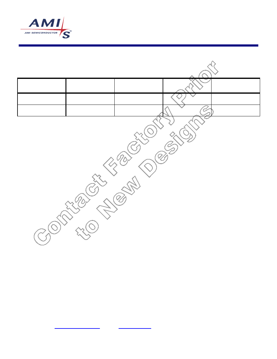
Table 5: 16-pin SOIC (0.150") Package Dimensions
DIMENSIONS
INCHES
MILLIMETERS
MIN.
MAX.
MIN.
MAX.
A
0.061
0.068
1.55
1.73
A1
0.004
0.0098
0.102
0.249
A2
0.055
0.061
1.40
1.55
B
0.013
0.019
0.33
0.49
C
0.0075
0.0098
0.191
0.249
D
0.386
0.393
9.80
9.98
E
0.150
0.157
3.81
3.99
e
0.050 BSC
1.27 BSC
H
0.230
0.244
5.84
6.20
h
0.010
0.016
0.25
0.41
L
0.016
0.035
0.41
0.89
0
∞
8
∞
0
∞
8
∞
B
e
D
A
1
SEATING PLANE
H
E
16
1
ALL RADII:
0.005" TO 0.01"
BASE PLANE
A
2
C
L
7∞ typ.
h x 45∞
A
AMERICAN MICROSYSTEMS, INC.
R
Table 6: 16-pin SOIC (0.150") Package Characteristics
PARAMETER
SYMBOL
CONDITIONS/DESCRIPTION
TYP.
UNITS
Thermal Impedance, Junction to Free-Air
16-pin 0.150" SOIC
JA
Air flow = 0 m/s
95
∞C/W
Corner lead
4.0
Lead Inductance, Self
L
11
Center lead
3.0
nH
Lead Inductance, Mutual
L
12
Any lead to any adjacent lead
0.4
nH
Lead Capacitance, Bulk
C
11
Any lead to V
SS
0.5
pF
5
3.1.02
FS6322-03
FS6322-03
FS6322-03
FS6322-03
Three-PLL Clock Generator IC
Three-PLL Clock Generator IC
Three-PLL Clock Generator IC
Three-PLL Clock Generator IC
5.0 Ordering
Information
ORDERING CODE
DEVICE NUMBER
PACKAGE TYPE
OPERATING
TEMPERATURE RANGE
SHIPPING
CONFIGURATION
11825-803
FS6322-03
16-pin (0.150") SOIC
(Small Outline Package)
0
∞
C to 70
∞
C (Commercial)
Tape and Reel
11825-813
FS6322-03
16-pin (0.150") SOIC
(Small Outline Package)
0
∞
C to 70
∞
C (Commercial)
Tubes
Copyright © 1999 American Microsystems, Inc.
Devices sold by AMI are covered by the warranty and patent indemnification provisions appearing in its Terms of Sale only. AMI
makes no warranty, express, statutory implied or by description, regarding the information set forth herein or regarding the freedom
of the described devices from patent infringement. AMI makes no warranty of merchantability or fitness for any purposes. AMI re-
serves the right to discontinue production and change specifications and prices at any time and without notice. AMI's products are
intended for use in commercial applications. Applications requiring extended temperature range, unusual environmental require-
ments, or high reliability applications, such as military, medical life-support or life-sustaining equipment, are specifically not recom-
mended without additional processing by AMI for such applications.
American Microsystems, Inc., 2300 Buckskin Rd., Pocatello, ID 83201, (208) 233-4690, FAX (208) 234-6796,
WWW Address:
http://www.amis.com
E-mail:
tgp@amis.com