 | –≠–ª–µ–∫—Ç—Ä–æ–Ω–Ω—ã–π –∫–æ–º–ø–æ–Ω–µ–Ω—Ç: FS6372 | –°–∫–∞—á–∞—Ç—å:  PDF PDF  ZIP ZIP |
IAmerican Microsystems, Inc., reserves the right to change the detail specifications as may be required to permit improvements in the design of its products.
3.1.02
FS6372
FS6372
FS6372
FS6372
ROM-Based 3-PLL Clock Generator IC
ROM-Based 3-PLL Clock Generator IC
ROM-Based 3-PLL Clock Generator IC
ROM-Based 3-PLL Clock Generator IC
ISO9001
ISO9001
ISO9001
ISO9001
1.0 Features
∑
Fully compatible with FS6370 (EEPROM-based) and
FS6377 (register-based) devices.
∑
Three on-chip PLLs with Reference and Feedback
Dividers set by internal ROM look-up table
∑
Four independently programmable muxes and post
dividers
∑
Selectable power-down of PLLs and shutdown of
output clock drivers
∑
Tristate outputs for board testing
∑
Can be optimized for reference clock (instead of
crystal) input
∑
5V to 3.3V operation
∑
Commercial (FS6372) and industrial (FS6372i) tem-
perature ranges
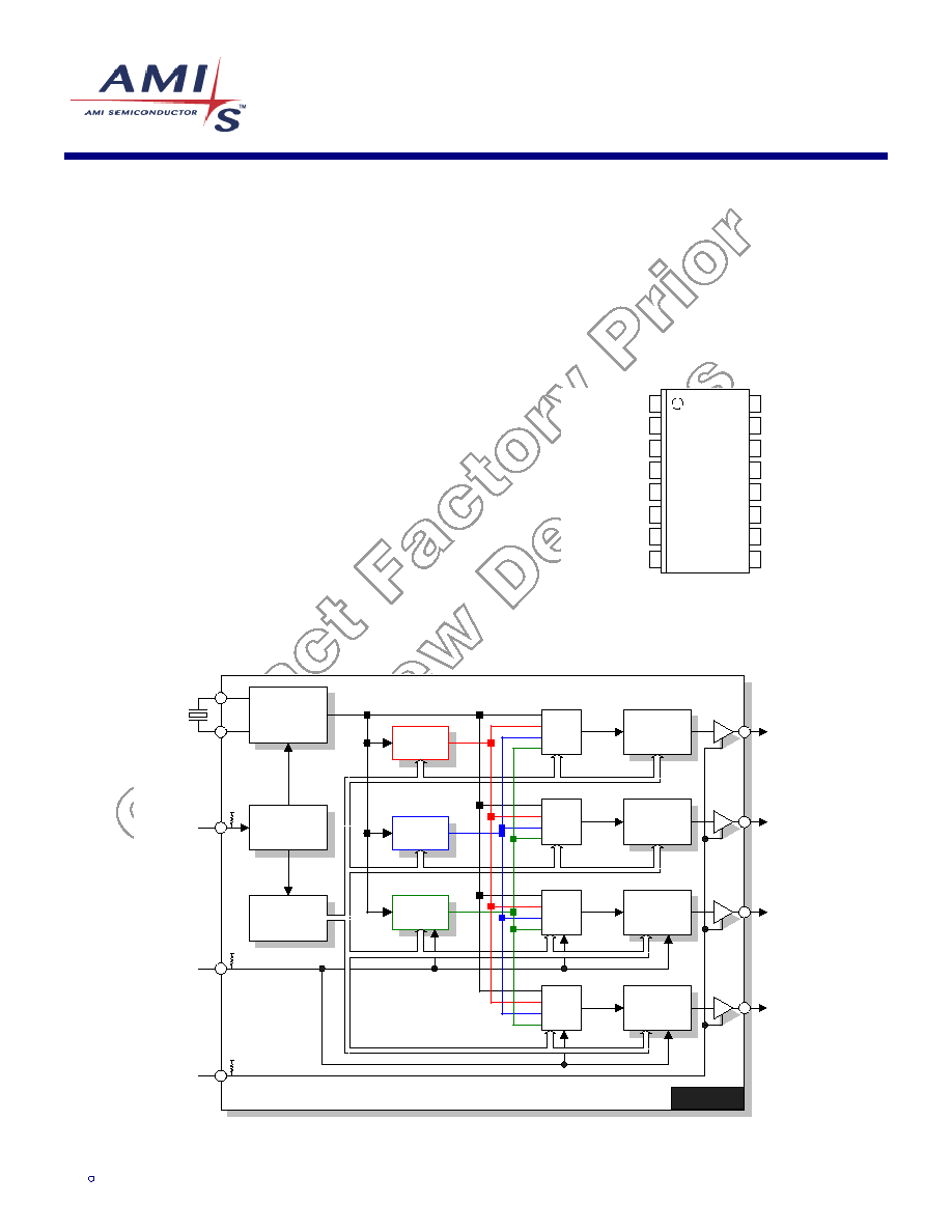
2.0 Description
The FS6372 is a CMOS clock generator IC designed to
minimize cost and component count in a variety of elec-
tronic systems. Three phase-locked loops feeding four
muxes and post dividers provide a high degree of flexibil-
ity.
Figure 1: Pin Configuration
1
16
2
3
4
5
6
7
8
15
14
13
12
11
10
9
VSS
SELECT
PD
VSS
XIN
XOUT/REFIN
OE
VDD
n/c
CLK_D
VSS
CLK_C
CLK_B
VDD
CLK_A
VDD
F
S
63
72-
xx
16-pin (0.150") SOIC
Figure 2: Block Diagram
ROM
Power Down
Control
Post
Divider C
Post
Divider B
FS6372
PD
Post
Divider A
CLK_A
CLK_B
CLK_C
Reference
Oscillator
PLL A
PLL B
XOUT
XIN
PLL C
Post
Divider D
CLK_D
SELECT
OE
Mux
A
Mux
B
Mux
C
Mux
D
3.1.02
FS6372
FS6372
FS6372
FS6372
ROM-Based 3-PLL Clock Generator IC
ROM-Based 3-PLL Clock Generator IC
ROM-Based 3-PLL Clock Generator IC
ROM-Based 3-PLL Clock Generator IC
Table 1: Pin Descriptions
Key: AI = Analog Input; AO = Analog Output; DI = Digital Input; DI
U
= Input with Internal Pull-Up; DI
D
= Input with Internal Pull-Down; DIO = Digital Input/Output; DI-3 = Three-Level Digital Input,
DO = Digital Output; P = Power/Ground; # = Active Low pin
PIN
TYPE
NAME
DESCRIPTION
1
P
VSS
Ground
2
DI
U
SELECT
Selects different device function (refer to specific variation of FS6372-xx for details)
3
DI
U
PD
Power-Down Input
4
P
VSS
Ground
5
AI
XIN
Crystal Oscillator Input
6
AO
XOUT / REFIN
Crystal Oscillator Output / Reference Clock Input
7
DI
U
OE
Output Enable Input
8
P
VDD
Power Supply (5V to 3.3V)
9
-
N/C
No Connect
10
DO
CLK_D
D Clock Output
11
P
VSS
Ground
12
DO
CLK_C
C Clock Output
13
DO
CLK_B
B Clock Output
14
P
VDD
Power Supply (5V to 3.3V)
15
DO
CLK_A
A Clock Output
16
P
VDD
Power Supply (5V to 3.3V)
3.1.02
3
FS6372
FS6372
FS6372
FS6372
ROM-Based 3-PLL Clock Generator IC
ROM-Based 3-PLL Clock Generator IC
ROM-Based 3-PLL Clock Generator IC
ROM-Based 3-PLL Clock Generator IC
ISO9001
ISO9001
ISO9001
ISO9001
3.0 Electrical
Specifications
Table 2: Absolute Maximum Ratings
Stresses above those listed under Absolute Maximum Ratings may cause permanent damage to the device. These conditions represent a stress rating only, and functional operation of the device at
these or any other conditions above the operational limits noted in this specification is not implied. Exposure to maximum rating conditions for extended conditions may affect device performance,
functionality, and reliability.
PARAMETER
SYMBOL
MIN.
MAX.
UNITS
Supply Voltage, dc (V
SS
= ground)
V
DD
V
SS
-0.5
7
V
Input Voltage, dc
V
I
V
SS
-0.5
V
DD
+0.5
V
Output Voltage, dc
V
O
V
SS
-0.5
V
DD
+0.5
V
Input Clamp Current, dc (V
I
< 0 or V
I
> V
DD
)
I
IK
-50
50
mA
Output Clamp Current, dc (V
I
< 0 or V
I
> V
DD
)
I
OK
-50
50
mA
Storage Temperature Range (non-condensing)
T
S
-65
150
∞C
Ambient Temperature Range, Under Bias
T
A
-55
125
∞C
Junction Temperature
T
J
150
∞C
Lead Temperature (soldering, 10s)
260
∞C
Input Static Discharge Voltage Protection (MIL-STD 883E, Method 3015.7)
2
kV
CAUTION: ELECTROSTATIC SENSITIVE DEVICE
Permanent damage resulting in a loss of functionality or performance may occur if this device is subjected to a high-energy elec-
trostatic discharge.
Table 3: Operating Conditions
PARAMETER
SYMBOL
CONDITIONS/DESCRIPTION
MIN.
TYP.
MAX.
UNITS
5V ± 10%
4.5
5
5.5
Supply Voltage
V
DD
3.3V ± 10%
3
3.3
3.6
V
Commercial
0
70
Ambient Operating Temperature Range
T
A
Industrial
-40
85
∞C
Crystal Resonator Frequency
f
XIN
5
27
MHz
Crystal Resonator Load Capacitance
C
XL
Parallel resonant, AT cut
18
pF
Output Driver Load Capacitance
C
L
15
pF

AMERICAN MICROSYSTEMS, INC.
March 2002
3.1.02
4
FS6372
FS6372
FS6372
FS6372
ROM-Based 3-PLL Clock Generator IC
ROM-Based 3-PLL Clock Generator IC
ROM-Based 3-PLL Clock Generator IC
ROM-Based 3-PLL Clock Generator IC
ISO9001
ISO9001
ISO9001
ISO9001
Table 4: DC Electrical Specifications
Unless otherwise stated, V
DD
= 5.0V ± 10%, no load on any output, and ambient temperature range T
A
= 0∞C to 70∞C. Parameters denoted with an asterisk ( * ) represent nominal characterization
data and are not currently production tested to any specific limits. MIN and MAX characterization data are
±
3
from typical. Negative currents indicate current flows out of the device.
PARAMETER
SYMBOL
CONDITIONS/DESCRIPTION
MIN.
TYP.
MAX.
UNITS
Overall
Supply Current, Dynamic, with
Loaded Outputs
I
DD
V
DD
= 5.5V, f
CLK
= 50MHz, C
L
= 15pF
43
mA
Supply Current, Static
I
DDL
V
DD
= 5.5V, device powered down
0.3
mA
Power-Down, Output Enable Pins (PD, OE)
V
DD
= 5.5V
3.85
V
DD
+0.3
High-Level Input Voltage
V
IH
V
DD
= 3.6V
2.52
V
DD
+0.3
V
V
DD
= 5.5V
V
SS
-0.3
1.65
Low-Level Input Voltage
V
IL
V
DD
= 3.6V
V
SS
-0.3
1.08
V
V
DD
= 5.5V
2.20
Hysteresis Voltage
V
hys
V
DD
= 3.6V
1.44
V
High-Level Input Current
I
IH
-1
1
µ
A
Low-Level Input Current (pull-up)
I
IL
V
IL
= 0V
-20
-36
-80
µ
A
Select (SELECT)
V
DD
= 5.5V
2.4
V
DD
+0.3
High-Level Input Voltage
V
IH
V
DD
= 3.6V
2.0
V
DD
+0.3
V
V
DD
= 5.5V
V
SS
-0.3
0.8
Low-Level Input Voltage
V
IL
V
DD
= 3.6V
V
SS
-0.3
0.8
V
High-Level Input Current
I
IH
-1
1
µ
A
Low-Level Input Current (pull-up)
I
IL
-20
-36
-80
µ
A
Crystal Oscillator Feedback (XIN)
V
DD
= 5.5V
2.9
Threshold Bias Voltage
V
TH
V
DD
= 3.6V
1.7
V
V
DD
= 5.5V
54
µ
A
High-Level Input Current
I
IH
V
DD
= 5.5V, oscillator powered down
5
15
mA
Low-Level Input Current
I
IL
V
DD
= 5.5V
-25
-54
-75
µ
A
Crystal Loading Capacitance *
C
L(xtal)
As seen by an external crystal connected to XIN and
XOUT
18
pF
Input Loading Capacitance *
C
L(XIN)
As seen by an external clock driver on XOUT; XIN
unconnected
36
pF
3.1.02
5
FS6372
FS6372
FS6372
FS6372
ROM-Based 3-PLL Clock Generator IC
ROM-Based 3-PLL Clock Generator IC
ROM-Based 3-PLL Clock Generator IC
ROM-Based 3-PLL Clock Generator IC
ISO9001
ISO9001
ISO9001
ISO9001
Table 5: DC Electrical Specifications, continued
Unless otherwise stated, V
DD
= 5.0V ± 10%, no load on any output, and ambient temperature range T
A
= 0∞C to 70∞C. Parameters denoted with an asterisk ( * ) represent nominal characterization
data and are not currently production tested to any specific limits. MIN and MAX characterization data are
±
3
from typical. Negative currents indicate current flows out of the device.
PARAMETER
SYMBOL
CONDITIONS/DESCRIPTION
MIN.
TYP.
MAX.
UNITS
Crystal Oscillator Drive (XOUT)
High-Level Output Source Current
I
OH
V
DD
= V(XIN) = 5.5V, V
O
= 0V
10
21
30
mA
Low-Level Output Sink Current
I
OL
V
DD
= 5.5V, V(XIN) = 0V, V
O
= 5.5V
-10
-21
-30
mA
Clock Outputs (CLK_A, CLK_B, CLK_C, CLK_D)
High-Level Output Source Current
I
OH
V
O
= 2.4V
-125
mA
Low-Level Output Sink Current
I
OL
V
O
= 0.4V
23
mA
z
OH
V
O
= 0.5V
DD
; output driving high
29
Output Impedance
z
OL
V
O
= 0.5V
DD
; output driving low
27
Tristate Output Current
I
Z
-10
10
µ
A
Short Circuit Source Current *
I
SCH
V
DD
= 5.5V, V
O
= 0V; shorted for 30s, max.
-150
mA
Short Circuit Sink Current *
I
SCL
V
DD
= V
O
= 5.5V, shorted for 30s, max.
123
mA
Figure 3: CLK_A, CLK_B, CLK_C, CLK_D Clock Outputs
Low Drive Current (mA)
High Drive Current (mA)
Voltage
(V)
MIN.
TYP.
MAX.
Voltage
(V)
MIN.
TYP.
MAX.
0
0
0
0
0
-87
-112
-150
0.2
9
11
12
0.5
-85
-110
-147
0.5
22
25
29
1
-83
-108
-144
0.7
29
34
40
1.5
-80
-104
-139
1
39
46
55
2
-74
-97
-131
1.2
44
52
64
2.5
-65
-88
-121
1.5
51
61
76
2.7
-61
-84
-116
1.7
55
66
83
3
-53
-77
-108
2
60
73
92
3.2
-48
-71
-102
2.2
62
77
97
3.5
-39
-62
-92
2.5
65
81
104
3.7
-32
-55
-85
2.7
65
83
108
4
-21
-44
-74
3
66
85
112
4.2
-13
-36
-65
3.5
67
87
117
4.5
0
-24
-52
4
68
88
119
4.7
-15
-43
4.5
69
89
120
5
0
-28
5
91
121
5.2
-11
5.5
123
5.5
0
-200
-150
-100
-50
0
50
100
150
-
0.5
1.0
1.5
2.0
2.5
3.0
3.5
4.0
4.5
5.0
5.5
O utput V oltage (V )
Output C
u
r
r
e
nt (mA
)
M IN
T YP
M AX
The data in this table represents nominal characterization data only.