
AMERICAN MICROSYSTEMS, INC.
July 2000
7.11.00
FS6477-02
FS6477-02
FS6477-02
FS6477-02
Three-PLL VCXO Programmable Clock Generator IC
Three-PLL VCXO Programmable Clock Generator IC
Three-PLL VCXO Programmable Clock Generator IC
Three-PLL VCXO Programmable Clock Generator IC
Preliminary Information
Preliminary Information
Preliminary Information
Preliminary Information
ISO9001
ISO9001
ISO9001
ISO9001
1.0 Features
�
3.3 volt operation (contact factory for 5 volt)
�
Fully user programmable via I
2
C
�
-bus serial interface
�
Three high-resolution, low-jitter PLLs optimized for
frequency synthesis
�
Additional multiplier PLL for generation of high-
frequency VCXO function from inexpensive funda-
mental mode crystals
�
Six CMOS clock outputs
�
Integrated VCXO circuitry for fine-tuning (typically +/-
100ppm) output frequencies
�
S0 and S1 control inputs can modify device power-up
function (see text)
�
Custom default frequency patterns, pinouts, and
packages are available. Contact your local AMI Sales
Representative for more information.
2.0 Description
The FS6477 is a CMOS clock generator IC designed to
minimize cost and component count in a variety of elec-
tronic systems. It is especially well suited to digital
video/audio systems such as digital set-top boxes.
Figure 1: Pin Configuration
1
16
2
3
4
5
6
7
8
15
14
13
12
11
10
9
SDA
VDD
VSS
XIN
XOUT
XTUNE
CLK_F/S1
CLK_E/S0
MODE
CLK_D
VSS
CLK_C
CLK_B
VDD
CLK_A
SCL
F
S
64
77
16-pin (0.150") SOIC
Figure 2: Block Diagram
Divider
Array
Device
Control
FS6477
VCXO +
Multiplier
XOUT
XIN
PLL A
PLL B
PLL C
CLK_A
CLK_B
CLK_C
CLK_D
XTUNE
CLK_E/S0
CLK_F/S1
I
2
C-bus
Interface
SCL
SDA
MODE

AMERICAN MICROSYSTEMS, INC.
July 2000
2
7.11.00
FS6477-02
FS6477-02
FS6477-02
FS6477-02
Three-PLL VCXO Programmable Clock Generator IC
Three-PLL VCXO Programmable Clock Generator IC
Three-PLL VCXO Programmable Clock Generator IC
Three-PLL VCXO Programmable Clock Generator IC
Preliminary Information
Preliminary Information
Preliminary Information
Preliminary Information
Table 1: Pin Descriptions
Key: AI = Analog Input; AO = Analog Output; DI = Digital Input; DI
U
= Input with Internal Pull-Up; DI
D
= Input with Internal Pull-Down; DIO = Digital Input/Output; DI-3 = Three-Level Digital Input,
DO = Digital Output; P = Power/Ground; # = Active Low pin
PIN
TYPE
NAME
DESCRIPTION
1
DI
U
O
SDA
Serial interface data input/output
2
P
VDD
Power supply (3.3V nominal)
3
P
VSS
Ground
4
AI
XIN
Voltage-controlled crystal oscillator feedback
5
AO
XOUT
Voltage-controlled crystal oscillator drive
6
AI
XTUNE
VCXO control voltage input
7
DI
U
O
CLK_F/S1
"F" clock output / S1 control input
8
DI
U
O
CLK_E/S0
"E" clock output / S0 control input
9
DI
U
MODE
Device MODE select (see text)
10
DO
CLK_D
"D" clock output
11
P
VSS
Ground
12
DO
CLK_C
"C" clock output
13
DO
CLK_B
"B" clock output
14
P
VDD
Power supply (5V to 3.3V)
15
DO
CLK_A
"A" clock output
16
DI
U
SCL
Serial interface clock input
AMERICAN MICROSYSTEMS, INC.
July 2000
3
7.11.00
Preliminary Information
Preliminary Information
Preliminary Information
Preliminary Information
FS6477-02
FS6477-02
FS6477-02
FS6477-02
Three-PLL VCXO Programmable Clock Generator IC
Three-PLL VCXO Programmable Clock Generator IC
Three-PLL VCXO Programmable Clock Generator IC
Three-PLL VCXO Programmable Clock Generator IC
3.0 Functional Block Description
3.1 Voltage-Controlled
Crystal
Oscillator (VCXO) and Multiplier
3.1.1 VCXO
The VCXO provides a tunable, low-jitter frequency ref-
erence for the rest of the FS6477 system components.
Load capacitors are internal to the FS6477. No exter-
nal components (other than the crystal itself) are re-
quired for operation of the VCXO.
Continuous fine-tuning of the VCXO frequency is ac-
complished by varying the voltage on the XTUNE pin.
Figure 3: Typical VCXO Characteristic
VCXO Deviation vs. XTUNE Input (typical)
-200
-150
-100
-50
0
50
100
150
200
250
0
0.5
1
1.5
2
2.5
3
V(XTUNE) - volts
D
e
v
i
at
ion
-
ppm
The oscillator operates the crystal resonator in the par-
allel-resonant mode. "Pulling" of the crystal oscillation
frequency is accomplished by altering the effective
load capacitance presented to the crystal. The actual
amount that changing the load capacitance alters the
oscillator frequency will depend on the characteristics
of the crystal as well as the oscillator circuit itself.
Specifically, the motional capacitance of the crystal
(usually referred to by crystal manufacturers as C
1
),
the static capacitance of the crystal (C
0
), and the load
capacitance (C
L
) of the oscillator determine the "pull-
ing" capability of the crystal in the oscillator circuit.
A simple formula to obtain the peak-to-peak "pulling"
capability of a crystal oscillator is:
(
)
(
) (
)
C
C
C
C
C
C
C
ppm
f
L
L
L
L
1
0
2
0
6
1
2
1
2
10
)
(
+
�
+
�
�
-
�
=
where C
L1
and C
L2
are the two extremes of the applied
load capacitance.
EXAMPLE: A crystal with the following parameters is
used. With C
1
= 0.02pF, C
0
= 6pF, C
L1
= 10pF, and C
L2
= 20pF, the tuning range (peak-to-peak) is
(
)
(
) (
)
ppm
.
f
300
10
6
20
6
2
106
10
20
025
0
=
+
�
+
�
�
-
�
=
.
3.1.2 Multiplier
A simple Phase-Locked Loop multiplies the output fre-
quency of the VCXO by eight for use by the program-
mable PLLs and Post Dividers. See below for a de-
scription of PLL operation.
3.2
Phase Locked Loops
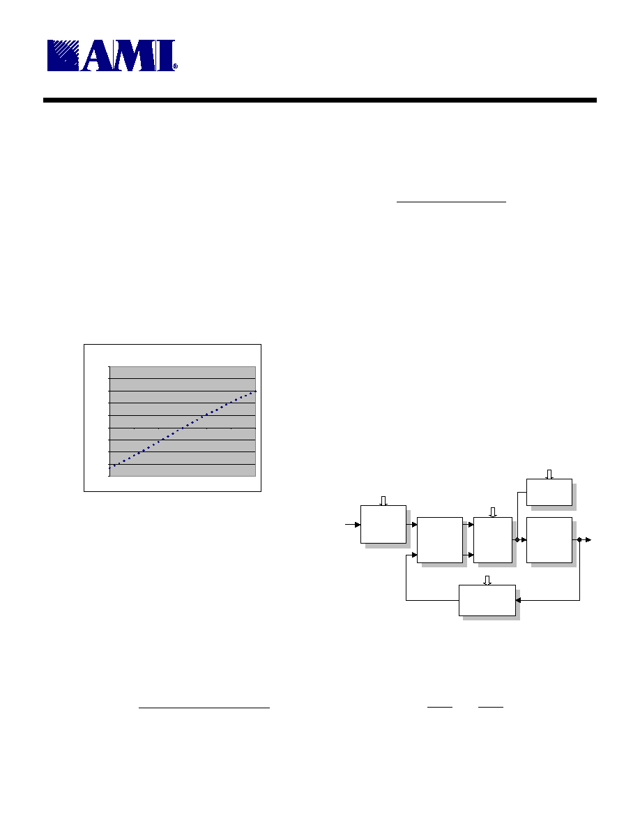
As shown in Figure 4, each PLL consists of a Refer-
ence Divider, a Phase-Frequency Detector (PFD), a
charge pump, an internal Loop Filter, a Voltage-
Controlled Oscillator (VCO), and a Feedback Divider.
This is a standard phase- and frequency-locked loop
architecture that multiplies a reference frequency to a
desired frequency by a ratio of integers. This frequency
multiplication is exact.
Figure 4: PLL Diagram
Reference
Divider
(N
R
)
Phase-
Frequency
Detector
Charge
Pump
UP
DOWN
Feedback
Divider
(N
F
)
Loop
Filter
REFDIV[7:0]
FBKDIV[10:0]
LFTC
CP
f
REF
f
VCO
Voltage
Controlled
Oscillator
The PFD compares the two frequencies at its input and
will drive the VCO to run faster (or slower) until both
frequencies are equal. When this condition has been
met:
�
�
�
�
�
�
�
�
=
�
�
�
�
�
�
�
�
R
REF
F
VCO
N
f
N
f
.

AMERICAN MICROSYSTEMS, INC.
July 2000
4
7.11.00
FS6477-02
FS6477-02
FS6477-02
FS6477-02
Three-PLL VCXO Programmable Clock Generator IC
Three-PLL VCXO Programmable Clock Generator IC
Three-PLL VCXO Programmable Clock Generator IC
Three-PLL VCXO Programmable Clock Generator IC
Preliminary Information
Preliminary Information
Preliminary Information
Preliminary Information
which can be re-arranged:
�
�
�
�
�
�
�
�
=
R
F
REF
VCO
N
N
f
f
.
3.2.1 Reference
Divider
The Reference Divider is designed for low phase jitter.
The divider accepts the output of the reference oscil-
lator and provides a divided-down frequency to the
PFD. The Reference Divider is an 8-bit divider, and
can be programmed for any modulus from 1 to 255 by
programming the equivalent binary value. A divide-by-
256 can also be achieved by programming the eight
bits to 00h.
3.2.2 Feedback
Divider
The Feedback Divider is based on a dual-modulus di-
vider (also called dual-modulus prescaler) technique.
It permits division by any integer value between 56 and
2047. Selected values below 56 are also permitted
(see Table).
Table 2: Feedback Modulus Below 56
FBKDIV[2:0]
FBKDIV[10:3]
000
001
010
011
100
101
110
111
00000001
8
9
-
-
-
-
-
-
00000010
16
17
18
-
-
-
-
-
00000011
24
25
26
27
-
-
-
-
00000100
32
33
34
35
36
-
-
-
00000101
40
41
42
43
44
45
-
-
00000110
48
49
50
51
52
53
54
-
00000111
56
57
58
59
60
61
62
63
FEEDBACK DIVIDER MODULUS
3.2.3 Post
Divider
The Post Divider is actually constructed of a cascade
of three programmable dividers, as shown in Figure 5.
Figure 5: Post Divider
Post
Divider 1
Post
Divider 2
Post
Divider 3
POSTCTL_x [3:0]
POST DIVIDER (N
P
)
Control ROM
f
IN
f
OUT
The modulus of the overall combination is controlled by
the appropriate register bits (see Table 7).
The Post Divider performs some useful functions. First,
it allows the VCO to be operated in a narrower range of
speeds compared to the output frequencies that are
needed in many applications. Second, the extra integer
in the denominator permits more flexibility in the pro-
gramming of the loop for many applications where fre-
quencies must be achieved exactly. It changes the
overall device frequency equation to:
�
�
�
�
�
�
�
�
�
�
�
�
�
�
�
�
=
P
R
F
REF
CLK
N
N
N
f
f
1
Note that a nominal 50/50 duty factor is always pre-
served (even for selections which have an odd
modulus).
3.3
Device Control Overview
The FS6477 contains an internal ROM that holds four
different device configurations. When the MODE pin is
LOW, the bi-directional pins (CLK_E/S0 and
CLK_F/S1) are made to be INPUTS and the voltage
levels applied to those pins select which one of those
four states is made active.
When the MODE pin is taken HIGH, the levels on
those pins are latched, and both bi-directional pins are
made to be OUTPUTS.
Any desired new configuration can be loaded into the
registers via the I2C interface at any time. The con-
figuration will not become applied to the PLLs or Post
Dividers until the appropriate SWAP bits have been set
to a "1".

AMERICAN MICROSYSTEMS, INC.
July 2000
A
FS6477-02
FS6477-02
FS6477-02
FS6477-02
Three-PLL VCXO Programmable Clock Generator IC
Three-PLL VCXO Programmable Clock Generator IC
Three-PLL VCXO Programmable Clock Generator IC
Three-PLL VCXO Programmable Clock Generator IC
Preliminary Information
Preliminary Information
Preliminary Information
Preliminary Information
ISO9001
ISO9001
ISO9001
ISO9001
Table 3: Programmable Register Map
Note: All programmable registers are cleared (set to "0") on power-up.
REGISTER
FUNCTION
BANK
BIT7
(MSB)
BIT6
BIT5
BIT4
BIT3
BIT2
BIT1
BIT0
(LSB)
0
SWAP
N/A
SWAP_7
SWAP_6
SWAP_5
SWAP_4
SWAP_3
SWAP_2
SWAP_1
SWAP_0
1
REFDIV_A[7:0]
2
FBKDIV_A[7:0]
3
PLLA
0
PLLPD_A
PLLSRC_
A
LFTC_A
CP_A
FBKDIV_A[10:8]
4
REFDIV_B[7:0]
5
FBKDIV_B[7:0]
6
PLLB
1
PLLPD_B
PLLSRC_
B
LFTC_B
CP_B
FBKDIV_B[10:8]
7
REFDIV_C[7:0]
8
FBKDIV_C[7:0]
9
PLLC
2
PLLPD_C
PLLSRC_
C
LFTC_C
CP_C
FBKDIV_C[10:8]
10
POSTDIVA
3
POSTPD_
A
POSTSRC_A[1:0]
POSTCTL_A[3:0]
11
POSTDIVB
4
POSTPD_
B
POSTSRC_B[1:0]
POSTCTL_B[3:0]
12
POSTDIVC
5
POSTPD_
C
POSTSRC_C[1:0]
POSTCTL_C[3:0]
13
POSTDIVD
6
POSTPD_
D
POSTSRC_D[1:0]
POSTCTL_D[3:0]
14
RESERV
ED
RESERV
ED
RESERV
ED
RESERV
ED
RESERV
ED
RESERV
ED
15
OUTPUT
7
CLKCTL
_F
CLKCTL
_E
CLKCTL
_D
CLKCTL
_C
CLKCTL
_B
CLKCTL
_A
Table 4: Device Default Frequencies
FS6477-02
frequencies assume 13.5MHz reference (10MHz < F_REF < 15MHz)
S1
S0
F(CLK_A)
F(CLK_B)
F(CLK_C)
F(CLK_D)
F(CLK_E)
F(CLK_F)
0
0
13.50000
13.50000
13.50000
27.00000
0
1
18.00000
18.00000
18.00000
27.00000
1
0
27.00000
27.00000
27.00000
27.00000
1
1
54.00000
54.00000
54.00000
27.00000
Always =
F(CLK_D)
Always =
F(CLK_D)