
American Microsystems, Inc. reserves the right to change the detail specifications as may be required to permit improvements in the design of its products.
2.4.03
FS7140 / FS7145
FS7140 / FS7145
FS7140 / FS7145
FS7140 / FS7145
Programmable Phase-Locked Loop Clock Generator
Programmable Phase-Locked Loop Clock Generator
Programmable Phase-Locked Loop Clock Generator
Programmable Phase-Locked Loop Clock Generator
ISO9001
ISO9001
ISO9001
ISO9001
1.0 Features
�
Extremely flexible and low-jitter phase-locked loop
(PLL) frequency synthesis
�
No external loop filter components needed
�
Configurable CMOS or pseudo-ECL outputs
�
Completely configurable via I
2
C
�
-bus
�
Up to four FS7140 or FS7145 can be used on a sin-
gle I
2
C-bus
�
3.3
volt
operation
�
Independent on-chip crystal oscillator and external
reference input
�
Very low "cumulative" jitter
Figure 1: Pin Configuration
1
16
2
3
4
5
6
7
8
15
14
13
12
11
10
9
IPRG
F
S
71
40
1
16
2
3
4
5
6
7
8
15
14
13
12
11
10
9
F
S
7140
n/c
VSS
REF
n/c
VDD
CLKP
CLKN
SCL
SDA
ADDR0
VSS
XIN
XOUT
ADDR1
VDD
1
16
2
3
4
5
6
7
8
15
14
13
12
11
10
9
IPRG
F
S
7
145
n/c
VSS
REF
SYNC
VDD
CLKP
CLKN
SCL
SDA
ADDR0
VSS
XIN
XOUT
ADDR1
VDD
16-pin (0.150
) SOIC
16-pin (5.3mm) SSOP
2.0 Description
The FS7140 / FS7145 is a monolithic CMOS clock gen-
erator/regenerator IC designed to minimize cost and
component count in a variety of electronic systems. Via
the I
2
C-bus interface, the FS714x can be adapted to
many clock generation requirements.
The length of the Reference and Feedback Dividers, their
fine granularity, and the flexibility of the Post Divider
make the FS714x the most flexible stand-alone phase-
locked loop (PLL) clock generator available.
3.0 Applications
�
Precision Frequency Synthesis
�
Low-Frequency
Clock
Multiplication
�
Video Line-Locked Clock Generation
�
Laser Beam Printers (FS7145)
Figure 2: Device Block Diagram
FS7140 / FS7145
Crystal
Oscillator
XOUT
XIN
Reference
Divider
(N
R
)
Phase-
Frequency
Detector
Charge
Pump
UP
DOWN
REF
Feedback
Divider
(N
F
)
Loop
Filter
I
2
C
Interface
SCL
SDA
ADDR[1:0]
Registers
IPRG
Post
Divider
(N
Px
)
Voltage
Controlled
Oscillator
CMOS/PECL
Output
CLKN
CLKP
SYNC
(FS7145 only)
Sync
Control

2
2.4.03
FS7140 / FS7145
FS7140 / FS7145
FS7140 / FS7145
FS7140 / FS7145
Programmable Phase-Locked Loop
Programmable Phase-Locked Loop
Programmable Phase-Locked Loop
Programmable Phase-Locked Loop Clock Generator
Clock Generator
Clock Generator
Clock Generator
ISO9001
ISO9001
ISO9001
ISO9001
Table 1: FS7140 Pin Descriptions
Key: AI = Analog Input; AO = Analog Output; DI = Digital Input; DI
U
= Input with Internal Pull-Up; DI
D
= Input with Internal Pull-Down; DIO = Digital Input/Output; DI-3 = Three-Level Digital Input,
DO = Digital Output; P = Power/Ground; # = Active Low pin
PIN
TYPE
NAME
DESCRIPTION
1
DI
SCL
Serial Interface Clock (requires an external pull-up)
2
DIO
SDA
Serial Interface Data Input/Output (requires an external pull-up)
3
DI
D
ADDR0
Address Select Bit "0"
4
P
VSS
Ground
5
AI
XIN
Crystal Oscillator Feedback
6
AO
XOUT
Crystal Oscillator Drive
7
DI
D
ADDR1
Address Select Bit "1"
8
P
VDD
Power Supply (+3.3V nominal)
9
AI
IPRG
PECL Current Drive Programming
10
-
n/c
No Connection
11
P
VSS
Ground
12
DI
U
REF
Reference Frequency Input
13
-
n/c
No Connection
14
P
VDD
Power Supply (+3.3V nominal)
15
DO
CLKP
Clock Output
16
DO
CLKN
Inverted Clock Output
Table 2: FS7145 Pin Descriptions
Key: AI = Analog Input; AO = Analog Output; DI = Digital Input; DI
U
= Input with Internal Pull-Up; DI
D
= Input with Internal Pull-Down; DIO = Digital Input/Output; DI-3 = Three-Level Digital Input,
DO = Digital Output; P = Power/Ground; # = Active Low pin
PIN
TYPE
NAME
DESCRIPTION
1
DI
SCL
Serial Interface Clock (requires an external pull-up)
2
DIO
SDA
Serial Interface Data Input/Output (requires an external pull-up)
3
DI
D
ADDR0
Address Select Bit "0"
4
P
VSS
Ground
5
AI
XIN
Crystal Oscillator Feedback
6
AO
XOUT
Crystal Oscillator Drive
7
DI
D
ADDR1
Address Select Bit "1"
8
P
VDD
Power Supply (+3.3V nominal)
9
AI
IPRG
PECL Current Drive Programming
10
-
n/c
No Connection
11
P
VSS
Ground
12
DI
U
REF
Reference Frequency Input
13
DI
U
SYNC
Synchronization Input
14
P
VDD
Power Supply (+3.3V nominal)
15
DO
CLKP
Clock Output
16
DO
CLKN
Inverted Clock Output
3
2.4.03
FS7140 / FS7145
FS7140 / FS7145
FS7140 / FS7145
FS7140 / FS7145
Programmable Phase-Locked Loop Clock Generator
Programmable Phase-Locked Loop Clock Generator
Programmable Phase-Locked Loop Clock Generator
Programmable Phase-Locked Loop Clock Generator
ISO9001
ISO9001
ISO9001
ISO9001
4.0 Functional Block Description
4.1
Phase-Locked Loop (PLL)
The Phase Locked Loop is a standard phase- and fre-
quency- locked loop architecture. The PLL consists of a
Reference Divider, a Phase-Frequency Detector (PFD), a
charge pump, an internal loop filter, a Voltage-Controlled
Oscillator (VCO), a Feedback Divider, and a Post Divider.
The reference frequency (generated by either the on-
board crystal oscillator or an external frequency source,
is first reduced by the Reference Divider. The integer
value that the frequency is divided by is called the
modulus, and is denoted as N
R
for the Reference Divider.
This divided reference is then fed into the PFD.
The VCO frequency is fed back to the PFD through the
Feedback Divider (the modulus is denoted by N
F
).
The PFD will drive the VCO up or down in frequency until
the divided reference frequency and the divided VCO
frequency appearing at the inputs of the PFD are equal.
The input/output relationship between the reference fre-
quency and the VCO frequency is then:
R
REF
F
VCO
N
f
N
f
=
.
This basic PLL equation can be rewritten as
�
�
�
�
�
�
�
�
=
R
F
REF
VCO
N
N
f
f
.
A Post-Divider (actually a series combination of three
post dividers) follows the PLL and the final equation for
device output frequency is:
�
�
�
�
�
�
�
�
�
�
�
�
�
�
�
�
=
Px
R
F
REF
CLK
N
N
N
f
f
1
4.1.1 Reference
Divider
The Reference Divider is designed for low phase jitter.
The divider accepts either the output of either the crystal
oscillator circuit or an external reference frequency. The
Reference Divider is a 12-bit divider, and can be pro-
grammed for any modulus from 1 to 4095 (divide by 1 not
available on date codes prior to 0108).
4.1.2 Feedback
Divider
The Feedback Divider is based on a dual-modulus divider
(also called dual-modulus prescaler) technique. It per-
mits division by any integer value between 12 and 16383.
Simply program the FBKDIV register with the binary
equivalent of the desired modulus. Selected moduli be-
low 12 are also permitted. Moduli of: 4, 5, 8, 9, and 10
are also allowed (4 and 5 are not available on date codes
prior to 0108).
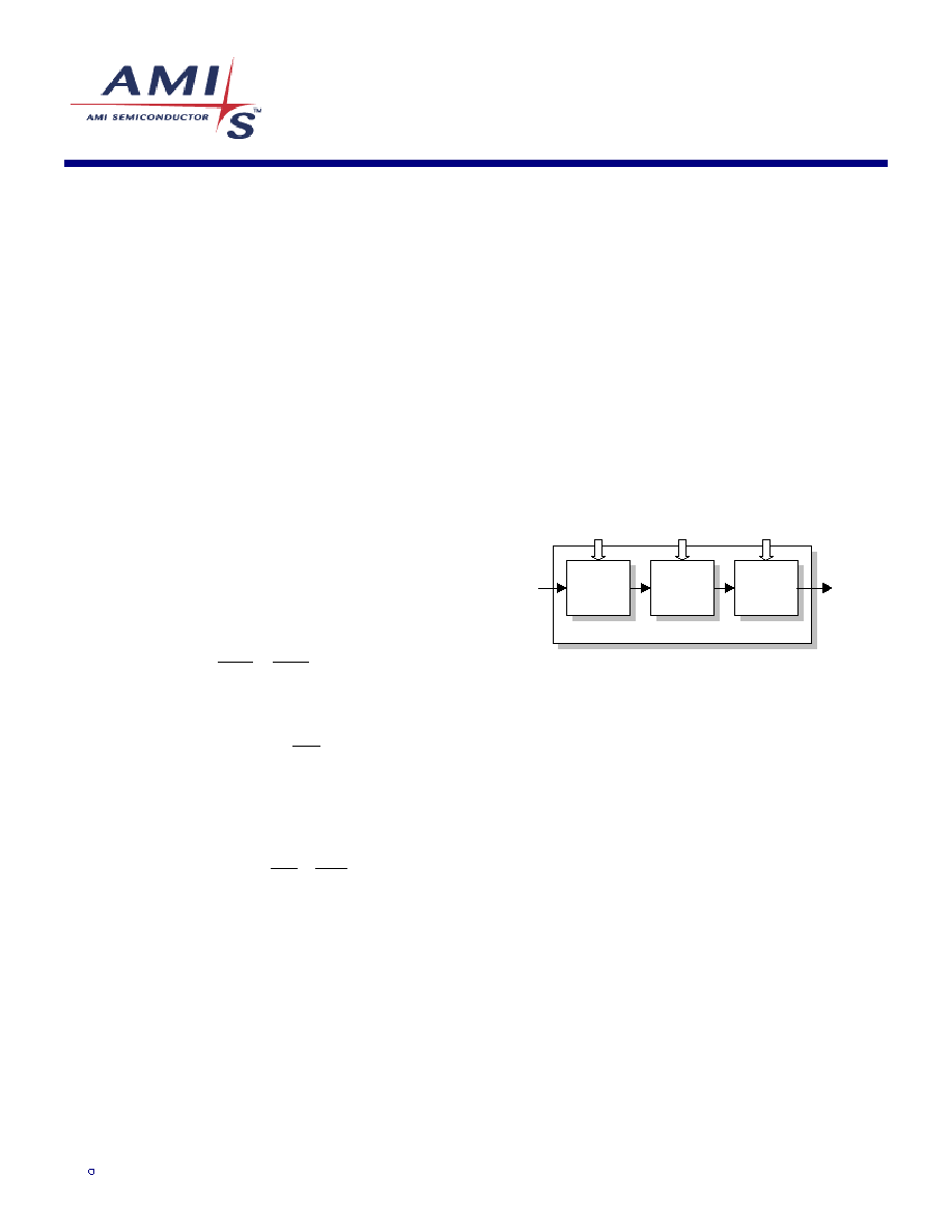
4.1.3 Post
Divider
The Post Divider consists of three individually program-
mable dividers, as shown in Figure 3.
Figure 3: Post Divider
Post
Divider 1
(N
P1
)
Post
Divider 2
(N
P2
)
Post
Divider 3
(N
P3
)
POST3[1:0]
POST2[3:0]
POST1[3:0]
POST DIVIDER (N
Px
)
f
CLK
f
VCO
The moduli of the individual dividers are denoted as N
P1
,
N
P2
, and N
P3
, and together they make up the array
modulus N
Px
.
3
2
1
P
P
P
Px
N
N
N
N
�
�
=
The Post Divider performs several useful functions. First,
it allows the VCO to be operated in a narrower range of
speeds compared to the variety of output clock speeds
that the device is required to generate. Second, the extra
integer in the denominator permits more flexibility in the
programming of the loop for many applications where
frequencies must be achieved exactly.
Note that a nominal 50/50 duty factor is always preserved
(even for selections which have an odd modulus).
See Table 8 for additional information.
4.1.4 Crystal
Oscillator
The FS7140 is equipped with a Pierce-type crystal oscil-
lator. The crystal is operated in parallel resonant mode.
Internal load capacitance is provided for the crystal.
While a recommended load capacitance for the crystal is
specified, crystals for other standard load capacitances
may be used if great precision of the reference frequency
(100ppm or less) is not required.

4
2.4.03
FS7140 / FS7145
FS7140 / FS7145
FS7140 / FS7145
FS7140 / FS7145
Programmable Phase-Locked Loop
Programmable Phase-Locked Loop
Programmable Phase-Locked Loop
Programmable Phase-Locked Loop Clock Generator
Clock Generator
Clock Generator
Clock Generator
ISO9001
ISO9001
ISO9001
ISO9001
4.1.5
Reference Divider Source MUX
The source of frequency for the Reference Divider can be
chosen to be the device Crystal Oscillator or the REF pin
by the REFDSRC bit.
When not using the Crystal Oscillator, it is preferred to
connect XIN to VSS. Do not connect to XOUT.
When not using the REF input, it is preferred to leave it
floating or connect to VDD.
4.1.6
Feedback Divider Source MUX
The source of frequency for the Feedback Divider may be
selected to be either the output of the Post-Divider or the
output of the Voltage-Controlled Oscillator by the
FBKDSRC bit.
Ordinarily, for frequency synthesis, the output of the VCO
is used. Use the output of the post-divider only where a
deterministic phase relationship between the output clock
and reference clock are desired (line-locked mode, for
example).
4.1.7 Device
Shutdown
Two bits are provided to effect shutdown of the device, if
desired, when it is not active. SHUT1 disables most ex-
ternally observable device functions. SHUT2 reduces
device quiescent current to absolute minimum values.
Normally, both bits should be set or cleared together.
Serial communications capability is not disabled by either
SHUT1 or SHUT2.
4.2
Differential Output Stage
The differential output stage supports both CMOS and
pseudo-ECL (PECL) signals. The desired output interface
is chosen via the programming registers.
If a PECL interface is used, the transmission line is usu-
ally terminated using a Th�venin termination. The output
stage can only sink current in the PECL mode, and the
amount of sink current is set by a programming resistor
on the LOCK/IPRG pin. The ratio of output sink current to
IPRG current is 13:1. Source current for the CLKx pins is
provided by the pull-up resistors that are part of the
Th�venin termination.
4.2.1 Example
Assume that it is desired to connect a PECL-type fanout
buffer right next to the FS7140.
Further assume:
�
V
DD
=3.3V
�
desired
V
HI
= 2.4V
�
desired
V
LO
= 1.6V
�
equivalent
R
LOAD
=75 ohms
Then:
R1 (from CLKP and CLKN output to VDD) =
R
LOAD
* V
DD
/ V
HI
=
75 * 3.3 / 2.4 =
103 ohms
R2 (from CLKP and CLKN output to GND) =
R
LOAD
* V
DD
/ (V
DD
- V
HI
) =
75 * 3.3 / (3.3 - 2.4) =
275 ohms
Rprgm (from VDD to IPRG pin) =
26 * (V
DD
* R
LOAD
) / (V
HI
- V
LO
) / 3 =
26 * (3.3 * 75) / (2.4 - 1.6) / 3 =
2.68 Kohms
4.3 SYNC
Circuitry
The FS7145 supports nearly instantaneous adjustment of
the output CLK phase by the SYNC input. Either edge
direction of SYNC (positive-going or negative-going) is
supported.
EXAMPLE (positive-going SYNC selected): Upon the
negative edge of SYNC input, a sequence begins to stop
the CLK output. Upon the positive edge, CLK resumes
operation, synchronized to the phase of the SYNC input
(plus a deterministic delay). This is performed by control
of the device post-divider. Phase resolution equal to � of
the VCO period can be achieved (approximately down to
2ns).
5
2.4.03
FS7140 / FS7145
FS7140 / FS7145
FS7140 / FS7145
FS7140 / FS7145
Programmable Phase-Locked Loop Clock Generator
Programmable Phase-Locked Loop Clock Generator
Programmable Phase-Locked Loop Clock Generator
Programmable Phase-Locked Loop Clock Generator
ISO9001
ISO9001
ISO9001
ISO9001
5.0 I
2
C-bus Control Interface
This device is a read/write slave device
meeting all Philips I
2
C-bus specifications
except a "general call." The bus has to be
controlled by a master device that generates
the serial clock SCL, controls bus access, and generates
the START and STOP conditions while the device works
as a slave. Both master and slave can operate as a
transmitter or receiver, but the master device determines
which mode is activated. A device that sends data onto
the bus is defined as the transmitter, and a device re-
ceiving data as the receiver.
I
2
C-bus logic levels noted herein are based on a percent-
age of the power supply (V
DD
). A logic-one corresponds
to a nominal voltage of V
DD
, while a logic-zero corre-
sponds to ground (V
SS
).
5.1 Bus
Conditions
Data transfer on the bus can only be initiated when the
bus is not busy. During the data transfer, the data line
(SDA) must remain stable whenever the clock line (SCL)
is high. Changes in the data line while the clock line is
high will be interpreted by the device as a START or
STOP condition. The following bus conditions are defined
by the I
2
C-bus protocol.
5.1.1 Not
Busy
Both the data (SDA) and clock (SCL) lines remain high to
indicate the bus is not busy.
5.1.2
START Data Transfer
A high to low transition of the SDA line while the SCL in-
put is high indicates a START condition. All commands to
the device must be preceded by a START condition.
5.1.3
STOP Data Transfer
A low to high transition of the SDA line while SCL is held
high indicates a STOP condition. All commands to the
device must be followed by a STOP condition.
5.1.4 Data
Valid
The state of the SDA line represents valid data if the SDA
line is stable for the duration of the high period of the SCL
line after a START condition occurs. The data on the
SDA line must be changed only during the low period of
the SCL signal. There is one clock pulse per data bit.
Each data transfer is initiated by a START condition and
terminated with a STOP condition. The number of data
bytes transferred between START and STOP conditions
is determined by the master device, and can continue
indefinitely. However, data that is overwritten to the de-
vice after the first eight bytes will overflow into the first
register, then the second, and so on, in a first-in, first-
overwritten fashion.
5.1.5 Acknowledge
When addressed, the receiving device is required to gen-
erate an Acknowledge after each byte is received. The
master device must generate an extra clock pulse to co-
incide with the Acknowledge bit. The acknowledging de-
vice must pull the SDA line low during the high period of
the master acknowledge clock pulse. Setup and hold
times must be taken into account.
The master must signal an end of data to the slave by not
generating and acknowledge bit on the last byte that has
been read (clocked) out of the slave. In this case, the
slave must leave the SDA line high to enable the master
to generate a STOP condition.
5.2 I
2
C-bus Operation
All programmable registers can be accessed randomly or
sequentially via this bi-directional two wire digital inter-
face. The crystal oscillator does not have to run for com-
munication to occur.
The device accepts the following I
2
C-bus commands:
5.2.1 Slave
Address
After generating a START condition, the bus master
broadcasts a seven-bit slave address followed by a R/W
bit. The address of the device is:
A6
A5
A4
A3
A2
A1
A0
1
0
1
1
0
X
X
where X is controlled by the logic level at the ADDR pins.
The selectable ADDR bits allow four different FS7140
devices to exist on the same bus. Note that every device
on an I
2
C-bus must have a unique address to avoid pos-
sible bus conflicts.