 | –≠–ª–µ–∫—Ç—Ä–æ–Ω–Ω—ã–π –∫–æ–º–ø–æ–Ω–µ–Ω—Ç: A29L040 | –°–∫–∞—á–∞—Ç—å:  PDF PDF  ZIP ZIP |

A29L040 Series
512K X 8 Bit CMOS 3.0 Volt-only,
Preliminary
Uniform Sector Flash Memory
PRELIMINARY (June, 2003, Version 0.1)
AMIC Technology, Corp.
Document Title
512K X 8 Bit CMOS 3.0 Volt-only, Uniform Sector Flash Memory
Revision History
Rev. No. History
Issue Date
Remark
0.0
Initial issue
December 10, 2002
Preliminary
0.1
Add 32-pin DIP package type
June 25, 2003

A29L040 Series
512K X 8 Bit CMOS 3.0 Volt-only,
Preliminary
Uniform Sector Flash Memory
PRELIMINARY (June, 2003, Version 0.1)
1
AMIC Technology, Corp.
Features
n
Single power supply operation
- Full voltage range: 2.7 to 3.6 volt read and write
operations for battery-powered applications
- Regulated voltage range: 3.0 to 3.6 volt read and
write operations for compatibility with high
performance 3.3 volt microprocessors
n
Access times:
- 70 (max.)
n
Current:
- 4 mA typical active read current
- 20 mA typical program/erase current
-
200 nA typical CMOS standby
-
200 nA Automatic Sleep Mode current
n
Flexible sector architecture
-
8 uniform sectors of 64 Kbyte each
-
Any combination of sectors can be erased
-
Supports full chip erase
-
Sector protection:
A hardware method of protecting sectors to prevent
any inadvertent program or erase operations within
that sector
n
Embedded Erase Algorithms
- Embedded Erase algorithm will automatically erase
the entire chip or any combination of designated
sectors and verify the erased sectors
- Embedded Program algorithm automatically writes
and verifies bytes at specified addresses
n
Typical 100,000 program/erase cycles per sector
n
20-year data retention at 125
∞
C
- Reliable operation for the life of the system
n
Compatible with JEDEC-standards
- Pinout and software compatible with single-power-
supply Flash memory standard
-
Superior inadvertent write protection
n
Data
Polling and toggle bits
-
Provides a software method of detecting completion
of program or erase operations
n
Erase Suspend/Erase Resume
-
Suspends a sector erase operation to read data
from, or program data to, a non-erasing sector, then
resumes the erase operation
n
Package options
-
32-pin DIP, PLCC, TSOP (8mm x 20mm) or sTSOP
(8mm x 14mm)
General Description
The A29L040 is a 3.0 volt-only Flash memory organized as
524,288 bytes of 8 bits each. The 512 Kbytes of data are
further divided into eight sectors of 64 Kbytes each for
flexible sector erase capability. The 8 bits of data appear on
I/O
0
- I/O
7
while the addresses are input on A0 to A18. The
A29L040 is offered in 32-pin PLCC, TSOP (8mm x 20mm)
or sTSOP (8mm x 14mm) packages. This device is
designed to be programmed in-system with the standard
system 3.0 volt VCC supply. Additional 12.0 volt VPP is not
required for in-system write or erase operations. However,
the A29L040 can also be programmed in standard EPROM
programmers.
The A29L040 has a second toggle bit, I/O
2
, to indicate
whether the addressed sector is being selected for erase,
and also offers the ability to program in the Erase Suspend
mode. The standard A29L040 offers access times of 70ns,
allowing high-speed microprocessors to operate without
wait states. To eliminate bus contention the device has
separate chip enable (
CE
), write enable (
WE
) and output
enable (
OE
) controls.
The device requires only a single 3.0 volt power supply for
both read and write functions. Internally generated and
regulated voltages are provided for the program and erase
operations.
The A29L040 is entirely software command set compatible
with the JEDEC single-power-supply Flash standard.
Commands are written to the command register using
standard microprocessor write timings. Register contents
serve as input to an internal state-machine that controls the
erase and programming circuitry. Write cycles also
internally latch addresses and data needed for the
programming and erase operations. Reading data out of the
device is similar to reading from other Flash or EPROM
devices.
Device programming occurs by writing the proper program
command sequence. This initiates the Embedded Program
algorithm - an internal algorithm that automatically times the
program pulse widths and verifies proper program margin.
Device erasure occurs by executing the proper erase
command sequence. This initiates the Embedded Erase
algorithm - an internal algorithm that automatically
preprograms the array (if it is not already programmed)
A29L040 Series
PRELIMINARY (June, 2003, Version 0.1)
2
AMIC Technology, Corp.
before executing the erase operation. During erase, the
device automatically times the erase pulse widths and
verifies proper erase margin.
The host system can detect whether a program or erase
operation is complete by reading the I/O
7
(
Data
Polling)
and I/O
6
(toggle) status bits. After a program or erase cycle
has been completed, the device is ready to read array data
or accept another command.
The sector erase architecture allows memory sectors to be
erased and reprogrammed without affecting the data
contents of other sectors. The A29L040 is fully erased when
shipped from the factory.
The hardware sector protection feature disables operations
for both program and erase in any combination of the
sectors of memory. This can be achieved via programming
equipment.
The Erase Suspend feature enables the user to put erase
on hold for any period of time to read data from, or program
data to, any other sector that is not selected for erasure.
True background erase can thus be achieved.
Power consumption is greatly reduced when the device is
placed in the standby mode.
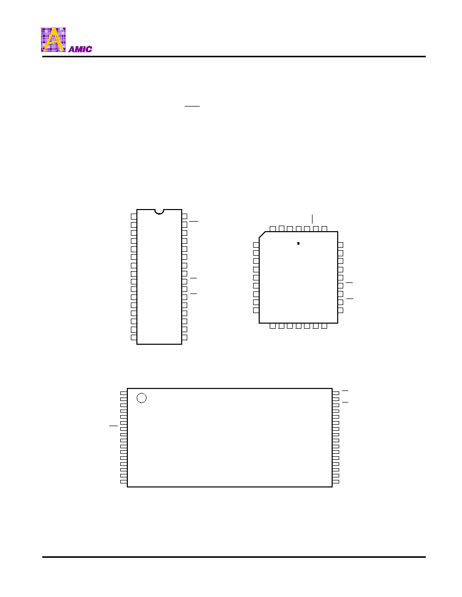
Pin Configurations
n
DIP
n
PLCC
A7
A6
A5
A4
A3
A2
A1
A0
I/O
0
21
22
23
24
25
26
27
28
29
12
13
11
8
9
5
7
6
CE
I/O
7
A10
A29L040L
OE
A11
A9
A8
A13
A14
I/O
1
I/O
2
VSS
I/O
3
I/O
4
I/O
5
I/O
6
4
3
2
1
32
31
30
A12
A15
A16
A18
VCC
WE
A17
14
15
16
17
18
19
20
10
A18
A16
A15
A12
A7
A6
A5
A4
A3
A2
A1
A0
I/O
0
I/O
1
I/O
2
I/O
3
VSS
I/O
4
I/O
5
I/O
6
I/O
7
CE
A10
OE
A9
A8
A13
WE
A17
A14
VCC
A11
A29L040
1
2
3
4
5
6
7
8
9
10
11
12
13
14
15
16
17
18
19
20
21
22
23
24
25
26
27
28
29
30
31
32
n
32-pin TSOP (8mm X 20mm)
n
32-pin sTSOP (8mm X 14mm)
A29L040V (8mm x 20mm)
A29L040X (8mm x 14mm)
1
2
3
4
5
6
7
8
9
10
11
12
13
14
15
16
A9
A8
A13
A14
A17
WE
VCC
A18
A16
A15
A12
A7
A6
A5
A4
32
31
30
29
28
27
26
25
24
23
22
21
20
19
18
17
A3
A2
A1
A0
I/O
0
I/O
1
I/O
2
VSS
I/O
3
I/O
4
I/O
5
I/O
6
I/O
7
CE
A10
OE
A11
A29L040 Series
PRELIMINARY (June, 2003, Version 0.1)
3
AMIC Technology, Corp.
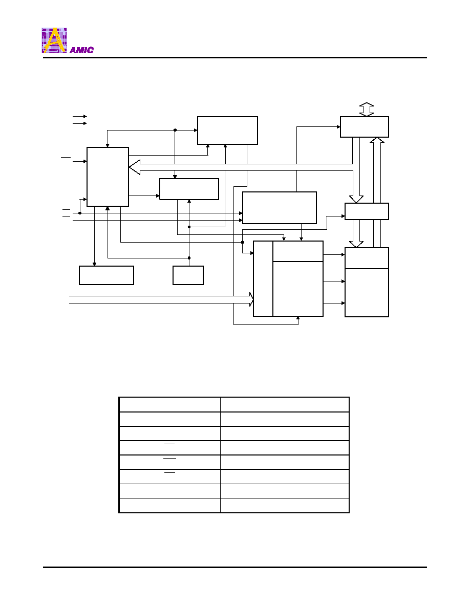
Block Diagram
Pin Descriptions
Pin No.
Description
A0 - A18
Address Inputs
I/O
0
- I/O
7
Data Inputs/Outputs
CE
Chip Enable
WE
Write Enable
OE
Output Enable
VSS
Ground
VCC
Power Supply
State
Control
Command
Register
Address Latch
X-decoder
Y-Decoder
Chip Enable
Output Enable
Logic
Cell Matrix
Y-Gating
VCC Detector
PGM Voltage
Generator
Data Latch
Input/Output
Buffers
Erase Voltage
Generator
VCC
VSS
WE
CE
OE
A0-A18
I/O
0
- I/O
7
Timer
STB
STB
A29L040 Series
PRELIMINARY (June, 2003, Version 0.1)
4
AMIC Technology, Corp.
Absolute Maximum Ratings*
Storage Temperature Plastic Packages . . . . . . . . . . . . . . .
. . . . . . . . . . . . . . . . . . . . . . . . . . . . . . . . . . .0
∞
C to + 70
∞
C
. . . . . . . . . . . . . . . . . . . . . . for -U series: -45
∞
C to +85
∞
C
Ambient Temperature with Power Applied . . . . . . . . . . . . .
. . . . . . . . . . . . . . . . . . . . . . . . . . . . . . . . . . 0
∞
C to + 70
∞
C
. . . . . . . . . . . . . . . . . . . . . . for -U series: -45
∞
C to +85
∞
C
Voltage with Respect to Ground
VCC (Note 1) . . . . . . . . . . . . . . . . . . . . . . . -0.5V to +4.0V
A9 &
OE
(Note 2) . . . . . . . . . . . . . . . . . . . . -0.5 to +12.5V
All other pins (Note 1) . . . . . . . . . . . . -0.5V to VCC + 0.5V
Output Short Circuit Current (Note 3) . . . . . . . . . 200mA
Notes:
1. Minimum DC voltage on input or I/O pins is -0.5V.
During voltage transitions, input or I/O pins may
undershoot VSS to -2.0V for periods of up to 20ns.
Maximum DC voltage on input and I/O pins is VCC
+0.2V. During voltage transitions, input or I/O pins may
overshoot to VCC +2.0V for periods up to 20ns.
2. Minimum DC input voltage on A9 and
OE
is -0.5V.
During voltage transitions, A9 and
OE
may overshoot
VSS to -2.0V for periods of up to 20ns. Maximum DC
input voltage on A9 is +12.5V which may overshoot to
14.0V for periods up to 20ns.
3. No more than one output is shorted at a time. Duration
of the short circuit should not be greater than one
second.
*Comments
Stresses above those listed under "Absolute Maximum
Ratings" may cause permanent damage to this device.
These are stress ratings only. Functional operation of
this device at these or any other conditions above
those indicated in the operational sections of these
specification is not implied or intended. Exposure to
the absolute maximum rating conditions for extended
periods may affect device reliability.
Operating Ranges
Commercial (C) Devices
Ambient Temperature (T
A
) . . . . . . . . . . . . . . 0
∞
C to +70
∞
C
Extended Range Devices
Ambient Temperature (T
A
) . . . . . . . . . . . . -45
∞
C to +85
∞
C
VCC Supply Voltages
VCC for all devices . . . . . . . . . . . . . . . . . . +2.7V to +3.6V
Operating ranges define those limits between which the
functionally of the device is guaranteed.
Device Bus Operations
This section describes the requirements and use of the
device bus operations, which are initiated through the
internal command register. The command register itself
does not occupy any addressable memory location. The
register is composed of latches that store the commands,
along with the address and data information needed to
execute the command. The contents of the register serve
as inputs to the internal state machine. The state machine
outputs dictate the function of the device. The appropriate
device bus operations table lists the inputs and control
levels required, and the resulting output. The following
subsections describe each of these operations in further
detail.
Table 1. A29L040 Device Bus Operations
Operation
CE
OE
WE
A0 ≠ A18
I/O
0
- I/O
7
Read
L
L
H
A
IN
D
OUT
Write
L
H
L
A
IN
D
IN
CMOS Standby
VCC
±
0.3 V
X
X
X
High-Z
TTL Standby
H
X
X
X
High-Z
Output Disable
L
H
H
X
High-Z
Legend:
L = Logic Low = V
IL
, H = Logic High = V
IH
, V
ID
= 12.0
±
0.5V, X = Don't Care, D
IN
= Data In, D
OUT
= Data Out, A
IN
= Address In
Note: See the "Sector Protection/Unprotection" section, for more information.