
A29L160A Series
2M X 8 Bit / 1M X 16 Bit CMOS 3.3 Volt-only,
Boot Sector Flash Memory
(May, 2005, Version 0.1)
AMIC Technology, Corp.
Document Title
2M X 8 Bit / 1M X 16 Bit CMOS 3.3 Volt-only, Boot Sector Flash Memory
Revision History
Rev. No. History Issue
Date Remark
0.0
Initial issue
April 1, 2005
Preliminary
0.1
Change Vcc_min from 2.7V to 3.0V
May 12, 2005

A29L160A Series
2M X 8 Bit / 1M X 16 Bit CMOS 3.3 Volt-only,
Boot Sector Flash Memory
(May, 2005, Version 0.1)
1
AMIC Technology, Corp.
Features
Single power supply operation
- Regulated voltage range: 3.0 to 3.6 volt read and write
operations for compatibility with high performance 3.3
volt microprocessors
Access times:
-
70/90
(max.)
Current:
- 9 mA typical active read current
- 20 mA typical program/erase current
-
200 nA typical CMOS standby
-
200 nA Automatic Sleep Mode current
Flexible sector architecture
-
16 Kbyte/ 8 KbyteX2/ 32 Kbyte/ 64 KbyteX31 sectors
-
8 Kword/ 4 KwordX2/ 16 Kword/ 32 KwordX31 sectors
-
Any combination of sectors can be erased
-
Supports full chip erase
-
Sector protection:
A hardware method of protecting sectors to prevent any
inadvertent program or erase operations within that
sector. Temporary Sector Unprotect feature allows code
changes in previously locked sectors
Unlock Bypass Program Command
- Reduces overall programming time when issuing
multiple program command sequence
Top or bottom boot block configurations available
Embedded Algorithms
- Embedded Erase algorithm will automatically erase the
entire chip or any combination of designated sectors and
verify the erased sectors
- Embedded Program algorithm automatically writes and
verifies data at specified addresses
Typical 100,000 program/erase cycles per sector
20-year data retention at 125
�
C
-
Reliable operation for the life of the system
CFI (Common Flash Interface) compliant
- Provides device-specific information to the system,
allowing host software to easily reconfigure for different
Flash devices
Compatible with JEDEC-standards
- Pinout and software compatible with single-power-supply
Flash memory standard
-
Superior inadvertent write protection
Data
Polling and toggle bits
-
Provides a software method of detecting completion of
program or erase operations
Ready /
BUSY
pin (RY /
BY
)
- Provides a hardware method of detecting completion of
program or erase operations (not available on 44-pin
SOP)
Erase Suspend/Erase Resume
-
Suspends a sector erase operation to read data from, or
program data to, a non-erasing sector, then resumes the
erase operation
Hardware reset pin (
RESET
)
-
Hardware method to reset the device to reading array
data
Package options
-
44-pin SOP or 48-pin TSOP (I) or 48-ball TFBGA
General Description
The A29L160A is a 16Mbit, 3.3 volt-only Flash memory
organized as 2,097,152 bytes of 8 bits or 1,048,576 words of
16 bits each. The 8 bits of data appear on I/O
0
- I/O
7
; the 16
bits of data appear on I/O
0
~I/O
15
. The A29L160A is offered in
48-ball FBGA,
44-pin SOP and 48-Pin TSOP packages. This
device is designed to be programmed in-system with the
standard system 3.3 volt VCC supply. Additional 12.0 volt
VPP is not required for in-system write or erase operations.
However, the A29L160A can also be programmed in
standard EPROM programmers.
The A29L160A has the first toggle bit, I/O
6
, which indicates
whether an Embedded Program or Erase is in progress, or it
is in the Erase Suspend. Besides the I/O
6
toggle bit, the
A29L160A has a second toggle bit, I/O
2
, to indicate whether
the addressed sector is being selected for erase. The
A29L160A also offers the ability to program in the Erase
Suspend mode. The standard A29L160A offers access times
of 70 and 90ns, allowing high-speed microprocessors to
operate without wait states. To eliminate bus contention the
device has separate chip enable (
CE
), write enable (
WE
)
and output enable (
OE
) controls.
The device requires only a single 3.3 volt power supply for
both read and write functions. Internally generated and
regulated voltages are provided for the program and erase
operations.
The A29L160A is entirely software command set compatible
with the JEDEC single-power-supply Flash standard.
Commands are written to the command register using
standard microprocessor write timings. Register contents
serve as input to an internal state-machine that controls the
erase and programming circuitry. Write cycles also internally
latch addresses and data needed for the programming and
erase operations. Reading data out of the device is similar to
reading from other Flash or EPROM devices.
Device programming occurs by writing the proper program
command sequence. This initiates the Embedded Program
algorithm - an internal algorithm that automatically times the
program pulse widths and verifies proper program margin.
A29L160A Series
(May, 2005, Version 0.1)
2
AMIC Technology, Corp.
Device erasure occurs by executing the proper erase
command sequence. This initiates the Embedded Erase
algorithm - an internal algorithm that automatically
preprograms the array (if it is not already programmed)
before executing the erase operation. During erase, the
device automatically times the erase pulse widths and
verifies proper erase margin. The Unlock Bypass mode
facilitates faster programming times by requiring only two
write cycles to program data instead of four.
The host system can detect whether a program or erase
operation is complete by observing the RY /
BY
pin, or
by
reading the I/O
7
(
Data
Polling) and I/O
6
(toggle) status bits.
After a program or erase cycle has been completed, the
device is ready to read array data or accept another
command.
The sector erase architecture allows memory sectors to be
erased and reprogrammed without affecting the data
contents of other sectors. The A29L160A is fully erased
when shipped from the factory.
The hardware sector protection feature disables operations
for both program and erase in any combination of the
sectors of memory. This can be achieved via programming
equipment.
The Erase Suspend/Erase Resume feature enables the user
to put erase on hold for any period of time to read data from,
or program data to, any other sector that is not selected for
erasure. True background erase can thus be achieved.
The hardware RESET pin terminates any operation in
progress and resets the internal state machine to reading
array data. The RESET pin may be tied to the system reset
circuitry. A system reset would thus also reset the device,
enabling the system microprocessor to read the boot-up
firmware from the Flash memory.
The device offers two power-saving features. When
addresses have been stable for a specified amount of time,
the device enters the automatic sleep mode. The system can
also place the device into the standby mode. Power
consumption is greatly reduced in both these modes.
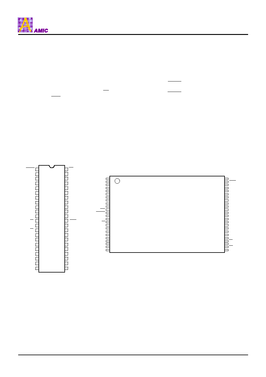
Pin Configurations
SOP
TSOP (I)
A18
A17
A7
A6
A5
A4
A3
A2
A1
A0
CE
VSS
OE
I/O
0
I/O
14
I/O
8
I/O
7
I/O
15
(A-1)
VSS
BYTE
A16
A15
A14
A12
A11
A10
A19
A8
A9
A13
A
2
9L
160A
M
1
2
3
4
5
6
7
8
9
10
11
12
13
14
15
16
29
30
31
32
33
34
35
36
37
38
39
40
41
42
43
44
RESET
WE
17
18
19
20
21
22
28
27
26
25
24
23
I/O
1
I/O
9
I/O
2
I/O
10
I/O
3
I/O
11
I/O
6
I/O
13
I/O
5
I/O
12
I/O
4
VCC
A29L160AV
1
2
3
4
5
6
7
8
9
10
11
12
13
14
15
16
A14
A13
A12
A11
A10
A9
A8
NC
WE
RESET
NC
NC
RY/BY
A18
48
47
46
45
44
43
42
41
40
39
38
37
36
35
34
33
I/O
2
I/O
10
I/O
3
I/O
11
VCC
I/O
4
I/O
12
I/O
5
I/O
13
I/O
6
I/O
14
I/O
7
I/O
15
(A-1)
VSS
BYTE
A16
A15
A19
17
18
19
20
21
22
23
24
25
26
27
28
29
30
31
32
I/O
9
I/O
1
I/O
8
I/O
0
OE
VSS
CE
A0
A17
A7
A6
A5
A4
A3
A2
A1
A29L160A Series
(May, 2005, Version 0.1)
3
AMIC Technology, Corp.
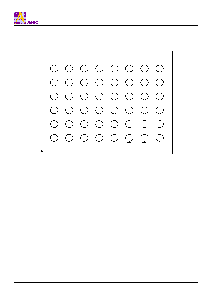
Pin Configurations (continued)
TFBGA
A6
B6
C6
D6
E6
F6
G6
H6
TFBGA
Top View, Balls Facing Down
A5
B5
C5
D5
E5
F5
G5
H5
A4
B4
C4
D4
E4
F4
G4
H4
A3
B3
C3
D3
E3
F3
G3
H3
A2
B2
C2
D2
E2
F2
G2
H2
A1
B1
C1
D1
E1
F1
G1
H1
A13
A12
A14
A15
A16
BYTE
I/O
15
(A-1)
VSS
A9
A8
A10
A11
I/O
7
I/O
14
I/O
13
I/O
6
WE
RESET
NC
A19
I/O
5
I/O
12
VCC
I/O
4
RY/BY
NC
A18
NC
I/O
2
I/O
10
I/O
11
I/O
3
A7
A17
A6
A5
I/O
0
I/O
8
I/O
9
I/O
1
A3
A4
A2
A1
A0
CE
OE
VSS

A29L160A Series
(May, 2005, Version 0.1)
4
AMIC Technology, Corp.
Block Diagram
Pin Descriptions
Pin No.
Description
A0 - A19
Address Inputs
I/O
0
- I/O
14
Data
Inputs/Outputs
I/O
15
Data Input/Output, Word Mode
I/O
15
(A-1)
A-1
LSB Address Input, Byte Mode
CE
Chip Enable
WE
Write Enable
OE
Output Enable
RESET
Hardware Reset
BYTE
Selects Byte Mode or Word Mode
RY/
BY
Ready/
BUSY
- Output
VSS Ground
VCC Power
Supply
NC
Pin not connected internally
State
Control
Command
Register
Address Lat
ch
X-decoder
Y-Decoder
Chip Enable
Output Enable
Logic
Cell Matrix
Y-Gating
VCC Detector
PGM Voltage
Generator
Data Latch
Input/Output
Buffers
Erase Voltage
Generator
VCC
VSS
WE
CE
OE
A0-A19
I/O
0
- I/O
15
(A-1)
Timer
STB
STB
RESET
Sector Switches
BYTE
RY/BY
A29L160A Series
(May, 2005, Version 0.1)
5
AMIC Technology, Corp.
Absolute Maximum Ratings*
Storage Temperature Plastic Packages. . . -65
�
C to + 150
�
C
Ambient Temperature with Power Applied. -55
�
C to + 125
�
C
Voltage with Respect to Ground
VCC (Note 1) . . . . . . . . . . . . . . . . . . . . ....... . -0.5V to +4.0V
A9,
OE
& RESET (Note 2) . . . . . . . . . . . .... -0.5 to +12.5V
All other pins (Note 1) . . . . . . . . . . .... . -0.5V to VCC + 0.5V
Output Short Circuit Current (Note 3) . . . . . . . .... . 200mA
Notes:
1. Minimum DC voltage on input or I/O pins is -0.5V. During
voltage transitions, input or I/O pins may undershoot VSS
to -2.0V for periods of up to 20ns. Maximum DC voltage
on input and I/O pins is VCC +0.5V. During voltage
transitions, input or I/O pins may
overshoot to VCC +2.0V
for periods up to 20ns.
2. Minimum DC input voltage on A9,
OE
and RESET is -
0.5V. During voltage transitions, A9,
OE
and RESET
may overshoot VSS to -2.0V for periods of up to 20ns.
Maximum DC input voltage on A9 is +12.5V which may
overshoot to 14.0V for periods up to 20ns.
3. No more than one output is shorted at a time. Duration of
the short circuit should not be greater than one second.
*Comments
Stresses above those listed under "Absolute Maximum
Ratings" may cause permanent damage to this device.
These are stress ratings only. Functional operation of
this device at these or any other conditions above
those indicated in the operational sections of these
specification is not implied or intended. Exposure to
the absolute maximum rating conditions for extended periods
may affect device reliability.
Operating Ranges
Commercial (C) Devices
Ambient Temperature (T
A
) . . . . . . . . . . . ..... . . 0
�
C to +70
�
C
Extended Range Devices
Ambient Temperature (T
A
)
For �I series. . . . . . . . . . . . . . . . . . . . . . . . . . -25
�
C to +85
�
C
For �U series . . . . . . . . . . . . . . . . . . . . . . . . . -40
�
C to +85
�
C
VCC Supply Voltages
VCC for all devices . . . . . . . . . . . . . . . . . ......+3.0V to +3.6V
Operating ranges define those limits between which the
functionally of the device is guaranteed.
Device Bus Operations
This section describes the requirements and use of the
device bus operations, which are initiated through the
internal command register. The command register itself does
not occupy any addressable memory location. The register is
composed of latches that store the commands, along with
the address and data information needed to
execute the command. The contents of the register serve as
inputs to the internal state machine. The state machine
outputs dictate the function of the device. The appropriate
device bus operations table lists the inputs and control levels
required, and the resulting output. The following subsections
describe each of these operations in further detail.
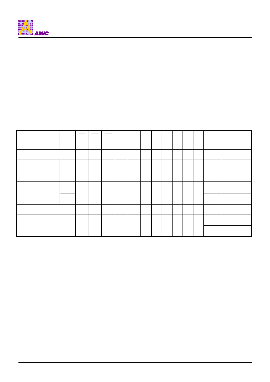
Table 1. A29L160A Device Bus Operations
I/O
8
- I/O
15
Operation
CE
OE
WE
RESET
A0 � A19
(Note 1)
I/O
0
- I/O
7
BYTE
=V
IH
BYTE
=V
IL
Read L
L
H
H
A
IN
D
OUT
D
OUT
I/O
8
~I/O
4
=High-Z
I/O
15
=A
-1
Write L
H
L
H
A
IN
D
IN
D
IN
High-Z
CMOS Standby
VCC
�
0.3 V
X X
VCC
�
0.3 V
X High-Z
High-Z
High-Z
Output Disable
L
H
H
H
X
High-Z
High-Z
High-Z
Hardware Reset
X
X
X
L
X
High-Z
High-Z
High-Z
Sector Protect
(See Note 2)
L H
L V
ID
Sector Address,
A6=L, A1=H, A0=L
D
IN
X
X
Sector Unprotect
(See Note 2)
L H
L V
ID
Sector Address,
A6=H, A1=H, A0=L
D
IN
X
X
Temporary Sector
Unprotect
X X
X V
ID
A
IN
D
IN
D
IN
X
Legend:
L = Logic Low = V
IL
, H = Logic High = V
IH
, V
ID
= 12.0
�
0.5V, X = Don't Care, D
IN
= Data In, D
OUT
= Data Out, A
IN
= Address In
Notes:
1. Addresses are A19:A0 in word mode (
BYTE
=V
IH
), A19: A
-1
in byte mode (
BYTE
=V
IL
).
2. See the "Sector Protection/Unprotection" section and Temporary Sector Unprotect for more information.

A29L160A Series
(May, 2005, Version 0.1)
6
AMIC Technology, Corp.
Word/Byte Configuration
The
BYTE
pin determines whether the I/O pins I/O
15
-I/O
0
operate in the byte or word configuration. If the
BYTE
pin is
set at logic "1", the device is in word configuration, I/O
15
-I/O
0
are active and controlled by
CE
and
OE
.
If the
BYTE
pin is set at logic "0", the device is in byte
configuration, and only I/O
0
-I/O
7
are active and controlled by
CE
and
OE
. I/O
8
-I/O
14
are tri-stated, and I/O
15
pin is used
as an input for the LSB(A-1) address function.
Requirements for Reading Array Data
To read array data from the outputs, the system must drive
the
CE
and
OE
pins to V
IL
.
CE
is the power control and
selects the device.
OE
is the output control and gates array
data to the output pins.
WE
should remain at V
IH
all the time
during read operation. The
BYTE
pin determines whether
the device outputs array data in words and bytes. The
internal state machine is set for reading array data upon
device power-up, or after a hardware reset. This ensures that
no spurious alteration of the memory content occurs during
the power transition. No command is necessary in this mode
to obtain array data. Standard microprocessor read cycles
that assert valid addresses on the device address inputs
produce valid data on the device data outputs. The device
remains enabled for read access until the command register
contents are altered.
See "Reading Array Data" for more information. Refer to the
AC Read Operations table for timing specifications and to the
Read Operations Timings diagram for the timing waveforms,
l
CC1
in the DC Characteristics table represents the active
current specification for reading array data.
Writing Commands/Command Sequences
To write a command or command sequence (which includes
programming data to the device and erasing sectors of
memory), the system must drive
WE
and
CE
to V
IL
, and
OE
to V
IH
. For program operations, the
BYTE
pin
determines whether the device accepts program data in
bytes or words, Refer to "Word/Byte Configuration" for more
information. The device features an Unlock Bypass mode to
facilitate faster programming. Once the device enters the
Unlock Bypass mode, only two write cycles are required to
program a word or byte, instead of four. The "
Word / Byte Program Command Sequence" section has
details on programming data to the device using both
standard and Unlock Bypass command sequence. An erase
operation can erase one sector, multiple sectors, or the
entire device. The Sector Address Tables indicate the
address range that each sector occupies. A "sector address"
consists of the address inputs required to uniquely select a
sector. See the "Command Definitions" section for details on
erasing a sector or the entire chip, or suspending/resuming
the erase operation.
After the system writes the autoselect command sequence,
the device enters the autoselect mode. The system can then
read autoselect codes from the internal register (which is
separate from the memory array) on I/O
7
- I/O
0
. Standard
read cycle timings apply in this mode. Refer to the
"Autoselect Mode" and "Autoselect Command Sequence"
sections for more information.
I
CC2
in the DC Characteristics table represents the active
current specification for the write mode. The "AC
Characteristics" section contains timing specification tables
and timing diagrams for write operations.
Program and Erase Operation Status
During an erase or program operation, the system may
check the status of the operation by reading the status bits
on I/O
7
- I/O
0
. Standard read cycle timings and I
CC
read
specifications apply. Refer to "Write Operation Status" for
more information, and to each AC Characteristics section for
timing diagrams.
Standby Mode
When the system is not reading or writing to the device, it
can place the device in the standby mode. In this mode,
current consumption is greatly reduced, and the outputs are
placed in the high impedance state, independent of the
OE
input.
The device enters the CMOS standby mode when the
CE
&
RESET pins are both held at VCC
�
0.3V. (Note that this is a
more restricted voltage range than V
IH
.) If
CE
and RESET
are held at V
IH
, but not within VCC
�
0.3V, the device will be
in the standby mode, but the standby current will be greater.
The device requires the standard access time (t
CE
) before it
is ready to read data.
If the device is deselected during erasure or programming,
the device draws active current until the operation is
completed.
I
CC3
and
I
CC4
in the DC Characteristics tables represent the
standby current specification.
Automatic Sleep Mode
The automatic sleep mode minimizes Flash device energy
consumption. The device automatically enables this mode
when addresses remain stable for t
ACC
+30ns. The automatic
sleep mode is independent of the
CE
,
WE
and
OE
control
signals. Standard address access timings provide new data
when addresses are changed. While in sleep mode, output
data is latched and always available to the system. I
CC4
in the
DC Characteristics table represents the automatic sleep
mode current specification.
Output Disable Mode
When the
OE
input is at V
IH
, output from the device is
disabled. The output pins are placed in the high impedance
state.
RESET
: Hardware Reset Pin
The RESET pin provides a hardware method of resetting
the device to reading array data. When the system drives the
RESET pin low for at least a period of t
RP
, the device
immediately terminates any operation in progress, tristates
all data output pins, and ignores all read/write attempts for
the duration of the RESET pulse. The device also resets the
internal state machine to reading array data. The operation
that was interrupted should be reinitiated once the device is
ready to accept another command sequence, to ensure data
integrity.
Current is reduced for the duration of the RESET pulse.
When RESET is held at VSS
�
0.3V, the device draws
CMOS standby current (I
CC4
). If RESET is held at V
IL
but not
within VSS
�
0.3V, the standby current will be greater.
A29L160A Series
(May, 2005, Version 0.1)
7
AMIC Technology, Corp.
The RESET pin may be tied to the system reset circuitry. A
system reset would thus also reset the Flash memory,
enabling the system to read the boot-up firmware from the
Flash memory.
If RESET is asserted during a program or erase operation,
the RY/
BY
pin remains a "0" (busy) until the internal reset
operation is complete, which requires a time t
READY
(during
Embedded Algorithms). The system can thus monitor
RY/
BY
to determine whether the reset operation is
complete. If RESET is asserted when a program or erase
operation is not executing (RY/
BY
pin is "1"), the reset
operation is completed within a time of t
READY
(not during
Embedded Algorithms). The system can read data t
RH
after
the RESET pin return to V
IH
.
Refer to the AC Characteristics tables for RESET
parameters and diagram.
Table 2. A29L160A Top Boot Block Sector Address Table
Address Range (in hexadecimal)
Sector A19 A18 A17 A16 A15 A14
A13
A12
Sector Size
(Kbytes/
Kwords)
Byte Mode
(x8)
Word Mode (x16)
SA0
0
0
0
0
0
X
X
X
64/32
000000 - 00FFFF
00000 - 07FFF
SA1
0
0
0
0
1
X
X
X
64/32
010000 - 01FFFF
08000 - 0FFFF
SA2
0
0
0
1
0
X
X
X
64/32
020000 - 02FFFF
10000 - 17FFF
SA3
0
0
0
1
1
X
X
X
64/32
030000 - 03FFFF
18000 - 1FFFF
SA4
0
0
1
0
0
X
X
X
64/32
040000 - 04FFFF
20000 - 27FFF
SA5
0
0
1
0
1
X
X
X
64/32
050000 - 05FFFF
28000 - 2FFFF
SA6
0
0
1
1
0
X
X
X
64/32
060000 - 06FFFF
30000 - 37FFF
SA7
0
0
1
1
1
X
X
X
64/32
070000 - 07FFFF
38000 - 3FFFF
SA8
0
1
0
0
0
X
X
X
64/32
080000 - 08FFFF
40000 - 47FFF
SA9
0
1
0
0
1
X
X
X
64/32
090000 - 09FFFF
48000 - 4FFFF
SA10
0
1
0
1
0
X
X
X
64/32
0A0000 - 0AFFFF
50000 - 57FFF
SA11
0
1
0
1
1
X
X
X
64/32
0B0000 - 0BFFFF
58000 - 5FFFF
SA12
0
1
1
0
0
X
X
X
64/32
0C0000 - 0CFFFF
60000 - 67FFF
SA13
0
1
1
0
1
X
X
X
64/32
0D0000 - 0DFFFF
68000 - 6FFFF
SA14
0
1
1
1
0
X
X
X
64/32
0E0000 - 0EFFFF
70000 - 77FFF
SA15
0
1
1
1
1
X
X
X
64/32
0F0000 - 0FFFFF
78000 - 7FFFF
SA16
1
0
0
0
0
X
X
X
64/32
100000 - 10FFFF
80000 - 87FFF
SA17
1
0
0
0
1
X
X
X
64/32
110000 - 11FFFF
88000 - 8FFFF
SA18
1
0
0
1
0
X
X
X
64/32
120000 - 12FFFF
90000 - 97FFF
SA19
1
0
0
1
1
X
X
X
64/32
130000 - 13FFFF
98000 - 9FFFF
SA20
1
0
1
0
0
X
X
X
64/32
140000 - 14FFFF
A0000 - A7FFF
SA21
1
0
1
0
1
X
X
X
64/32
150000 - 15FFFF
A8000 - AFFFF
SA22
1
0
1
1
0
X
X
X
64/32
160000 - 16FFFF
B0000 - B7FFF
SA23
1
0
1
1
1
X
X
X
64/32
170000 - 17FFFF
B8000 - BFFFF
SA24
1
1
0
0
0
X
X
X
64/32
180000 - 18FFFF
C0000 - C7FFF
SA25
1
1
0
0
1
X
X
X
64/32
190000 - 19FFFF
C8000 - CFFFF
SA26
1
1
0
1
0
X
X
X
64/32
1A0000 - 1AFFFF
D0000 - D7FFF
SA27
1
1
0
1
1
X
X
X
64/32
1B0000 - 1BFFFF
D8000 - DFFFF
SA28
1
1
1
0
0
X
X
X
64/32
1C0000 - 1CFFFF
E0000 - E7FFF
SA29
1
1
1
0
1
X
X
X
64/32
1D0000 - 1DFFFF
E8000 - EFFFF
SA30
1
1
1
1
0
X
X
X
64/32
1E0000 - 1EFFFF
F0000 - F7FFF
SA31
1
1
1
1
1
0
X
X
32/16
1F0000 - 1F7FFF
F8000 - FBFFF
SA32
1
1
1
1
1
1
0
0
8/4
1F8000 - 1F9FFF
FC000 - FCFFF
SA33
1
1
1
1
1
1
0
1
8/4
1FA000 - 1FBFFF
FD000 - FDFFF
SA34 1 1 1 1 1 1 1 X 16/8 1FC000 - 1FFFFF
FE000 - FFFFF
Note:
Address range is A19 : A
-1
in byte mode and A19 : A0 in word mode. See "Word/Byte Configuration" section.

A29L160A Series
(May, 2005, Version 0.1)
8
AMIC Technology, Corp.
Table 3. A29L160A Bottom Boot Block Sector Address Table
Address Range (in hexadecimal)
Sector A19 A18 A17 A16 A15 A14
A13
A12
Sector Size
(Kbytes/
Kwords)
Byte Mode (x8)
Word Mode (x16)
SA0
0
0
0
0
0
0
0
X
16/8
000000 - 003FFF
00000 - 01FFF
SA1
0
0
0
0
0
0
1
0
8/4
004000 - 005FFF
02000 - 02FFF
SA2
0
0
0
0
0
0
1
1
8/4
006000 - 007FFF
03000 - 03FFF
SA3
0
0
0
0
0
1
X
X
32/16
008000 - 00FFFF
04000 - 07FFF
SA4
0
0
0
0
1
X
X
X
64/32
010000 - 01FFFF
08000 - 0FFFF
SA5
0
0
0
1
0
X
X
X
64/32
020000 - 02FFFF
10000 - 17FFF
SA6
0
0
0
1
1
X
X
X
64/32
030000 - 03FFFF
18000 - 1FFFF
SA7
0
0
1
0
0
X
X
X
64/32
040000 - 04FFFF
20000 - 27FFF
SA8
0
0
1
0
1
X
X
X
64/32
050000 - 05FFFF
28000 - 2FFFF
SA9
0
0
1
1
0
X
X
X
64/32
060000 - 06FFFF
30000 - 37FFF
SA10
0
0
1
1
1
X
X
X
64/32
070000 - 07FFFF
38000 - 3FFFF
SA11
0
1
0
0
0
X
X
X
64/32
080000 - 08FFFF
40000 - 47FFF
SA12
0
1
0
0
1
X
X
X
64/32
090000 - 09FFFF
48000 - 4FFFF
SA13
0
1
0
1
0
X
X
X
64/32
0A0000 - 0AFFFF
50000 - 57FFF
SA14
0
1
0
1
1
X
X
X
64/32
0B0000 - 0BFFFF
58000 - 5FFFF
SA15
0
1
1
0
0
X
X
X
64/32
0C0000 - 0CFFFF
60000 - 67FFF
SA16
0
1
1
0
1
X
X
X
64/32
0D0000 - 0DFFFF
68000 - 6FFFF
SA17
0
1
1
1
0
X
X
X
64/32
0E0000 - 0EFFFF
70000 - 77FFF
SA18
0
1
1
1
1
X
X
X
64/32
0F0000 - 0FFFFF
78000 - 7FFFF
SA19
1
0
0
0
0
X
X
X
64/32
100000 - 10FFFF
80000 - 87FFF
SA20
1
0
0
0
1
X
X
X
64/32
110000 - 11FFFF
88000 - 8FFFF
SA21
1
0
0
1
0
X
X
X
64/32
120000 - 12FFFF
90000 - 97FFF
SA22
1
0
0
1
1
X
X
X
64/32
130000 - 13FFFF
98000 - 9FFFF
SA23
1
0
1
0
0
X
X
X
64/32
140000 - 14FFFF
A0000 - A7FFF
SA24
1
0
1
0
1
X
X
X
64/32
150000 - 15FFFF
A8000 - AFFFF
SA25
1
0
1
1
0
X
X
X
64/32
160000 - 16FFFF
B0000 � B7FFF
SA26
1
0
1
1
1
X
X
X
64/32
170000 - 17FFFF
B8000 - BFFFF
SA27
1
1
0
0
0
X
X
X
64/32
180000 - 18FFFF
C0000 - C7FFF
SA28
1
1
0
0
1
X
X
X
64/32
190000 - 19FFFF
C8000 - CFFFF
SA29
1
1
0
1
0
X
X
X
64/32
1A0000 - 1AFFFF
D0000 - D7FFF
SA30
1
1
0
1
1
X
X
X
64/32
1B0000 - 1BFFFF
D8000 - DFFFF
SA31
1
1
1
0
0
X
X
X
64/32
1C0000 - 1CFFFF
E0000 - E7FFF
SA32
1
1
1
0
1
X
X
X
64/32
1D0000 - 1DFFFF
E8000 - EFFFF
SA33
1
1
1
1
0
X
X
X
64/32
1E0000 - 1EFFFF
F0000 - F7FFF
SA34
1
1
1
1
1
X
X
X
64/32
1F0000 - 1FFFFF
F8000 - FFFFF
Note:
Address range is A19 : A
-1
in byte mode and A19 : A0 in word mode. See "Word/Byte Configuration" section.
A29L160A Series
(May, 2005, Version 0.1)
9
AMIC Technology, Corp.
Autoselect Mode
The autoselect mode provides manufacturer and device
identification, and sector protection verification, through
identifier codes output on I/O
7
- I/O
0
. This mode is primarily
intended for programming equipment to automatically match
a device to be programmed with its corresponding
programming algorithm. However, the autoselect codes can
also be accessed in-system through the command register.
When using programming equipment, the autoselect mode
requires V
ID
(11.5V to 12.5 V) on address pin A9. Address
pins A6, A1, and A0 must be as shown in Autoselect Codes
(High Voltage Method) table. In addition, when
verifying sector protection, the sector address must appear
on the appropriate highest order address bits. Refer to the
corresponding Sector Address Tables. The Command
Definitions table shows the remaining address bits that are
don't care. When all necessary bits have been set as
required, the programming equipment may then read the
corresponding identifier code on I/O
7
- I/O
0
.To access the
autoselect codes in-system, the host system can issue the
autoselect command via the command register, as shown in
the Command Definitions table. This method does not
require V
ID
. See "Command Definitions" for details on using
the autoselect mode.
Table 4. A29L160A Autoselect Codes (High Voltage Method)
Description
Mode
CE
OE
WE
A19
to
A12
A11
to
A10
A9
A8
to
A7
A6
A5
to
A2
A1
A0 I/O
8
to
I/O
15
I/O
7
to
I/O
0
Manufacturer ID: AMIC
L
L
H
X
X
V
ID
X
L
X
L
L X
37h
Word
22h C4h
Device ID:
A29L160A
(Top Boot Block)
Byte
L L H X X
V
ID
X
L
X
L
H
X C4h
Word
22h 49h
Device ID:
A29L160A
(Bottom Boot Block)
Byte
L L H X X
V
ID
X
L
X
L
H
X 49h
Continuation ID
L
L
H
X
X
V
ID
X
L
X
H
H X
7Fh
X
01h
(protected)
Sector Protection Verification
L
L
H
SA
X
V
ID
X
L
X
H
L
X
00h
(unprotected)
L=Logic Low= V
IL
, H=Logic High=V
IH
, SA=Sector Address, X=Don't Care.
Note: The autoselect codes may also be accessed in-system via command sequences.
A29L160A Series
(May, 2005, Version 0.1)
10
AMIC Technology, Corp.
Sector Protection/Unprotection
The hardware sector protection feature disables both
program and erase operations in any sector. The hardware
sector unprotection feature re-enables both program and
erase operations in previously protected sectors.
It is possible to determine whether a sector is protected or
unprotected. See "Autoselect Mode" for details.
Sector protection / unprotection can be implemented via two
methods. The primary method requires VID on the
RESET pin only, and can be implemented either in-system or
via programming equipment. Figure 2 shows the algorithm
and the Sector Protect / Unprotect Timing Diagram illustrates
the timing waveforms for this feature. This method uses
standard microprocessor bus cycle timing. For sector
unprotect, all unprotected sectors must first be protected
prior to the first sector unprotect write cycle. The alternate
method must be implemented using programming
equipment. The procedure requires a high voltage (V
ID
) on
address pin A9 and the control pins.
The device is shipped with all sectors unprotected.
It is possible to determine whether a sector is protected or
unprotected. See "Autoselect Mode" for details.
Hardware Data Protection
The requirement of command unlocking sequence for
programming or erasing provides data protection against
inadvertent writes (refer to the Command Definitions table).
In addition, the following hardware data protection measures
prevent accidental erasure or programming, which might
otherwise be caused by spurious system level signals during
V
CC
power-up transitions, or from system noise. The device
is powered up to read array data to avoid accidentally writing
data to the array.
Write Pulse "Glitch" Protection
Noise pulses of less than 5ns (typical) on
OE
,
CE
or
WE
do not initiate a write cycle.
Logical Inhibit
Write cycles are inhibited by holding any one of
OE
=V
IL
,
CE
= V
IH
or
WE
= V
IH
. To initiate a write cycle,
CE
and
WE
must be a logical zero while
OE
is a logical one.
Power-Up Write Inhibit
If
WE
=
CE
= V
IL
and
OE
= V
IH
during power up, the
device does not accept commands on the rising edge of
WE
. The internal state machine is automatically reset to
reading array data on the initial power-up.
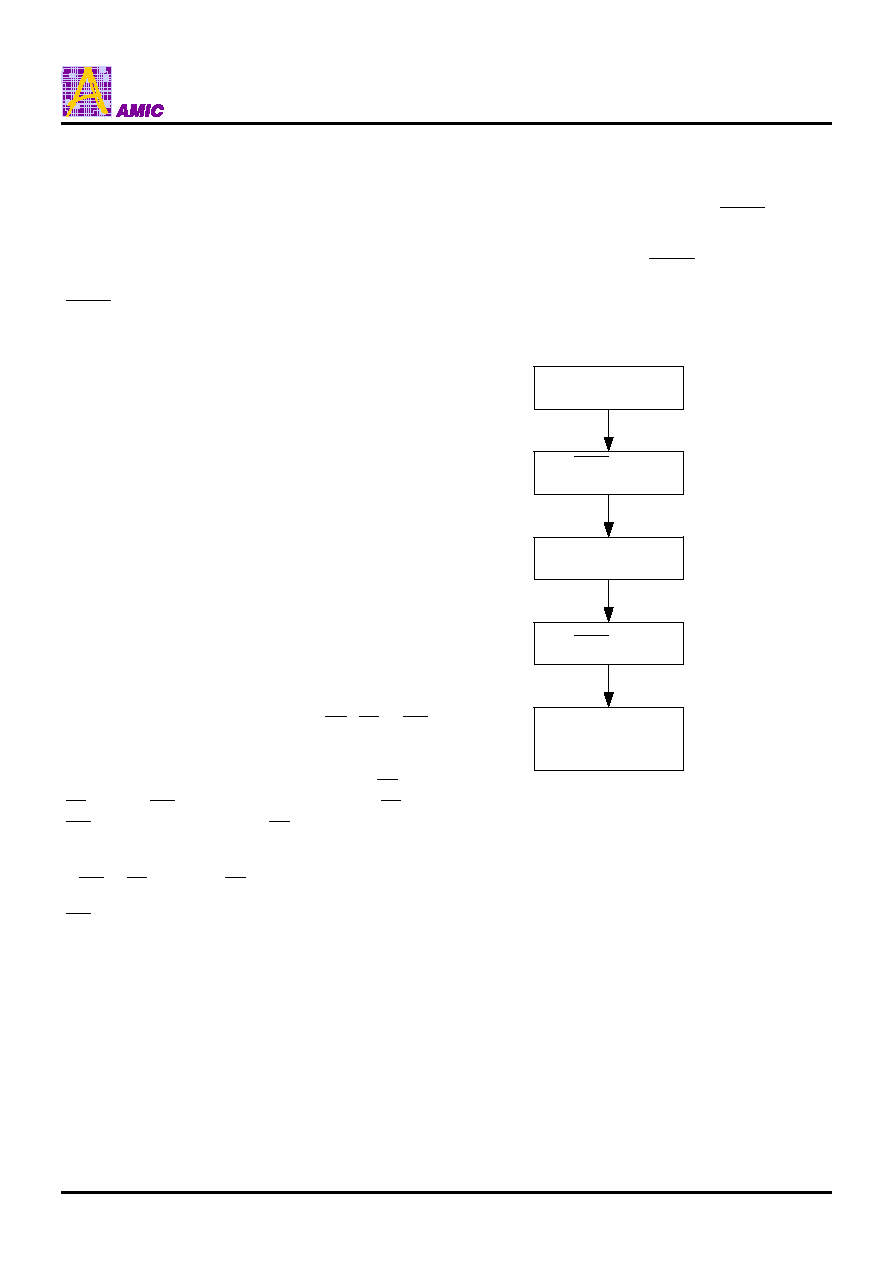
Temporary Sector Unprotect
This feature allows temporary unprotection of previous
protected sectors to change data in-system. The Sector
Unprotect mode is activated by setting the RESET pin to V
ID
.
During this mode, formerly protected sectors can be
programmed or erased by selecting the sector addresses.
Once V
ID
is removed from the RESET pin, all the previously
protected sectors are protected again. Figure 1 shows the
algorithm, and the Temporary Sector Unprotect diagram
shows the timing waveforms, for this feature.
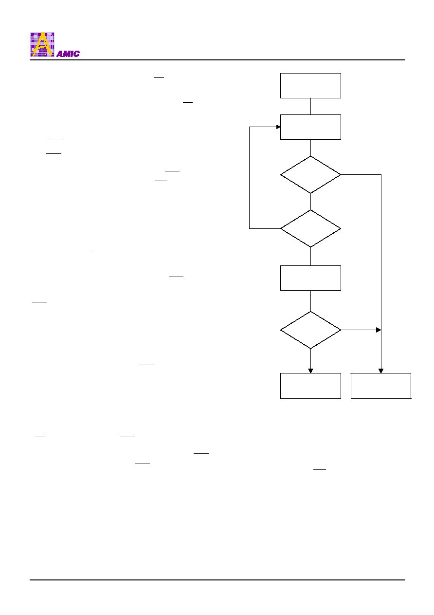
START
RESET = V
ID
(Note 1)
Perform Erase or
Program Operations
RESET = V
IH
Temporary Sector
Unprotect
Completed (Note 2)
Notes:
1. All protected sectors unprotected.
2. All previously protected sectors are protected once again.
Figure 1. Temporary Sector Unprotect Operation

A29L160A Series
(May, 2005, Version 0.1)
11
AMIC Technology, Corp.
START
PLSCNT=1
RESET=V
ID
Wait 1 us
First Write
Cycle=60h?
Set up sector
address
Sector Protec:
Write 60h to sector
address with A6=0,
A1=1, A0=0
Wait 150 us
Verify Sector
Protect: Write 40h
to sector address
with A6=0, A1=1,
A0=0
Read from
sector address
with A6=0,
A1=1, A0=0
Data=01h?
Protect another
sector?
Remove V
ID
from RESET
Write reset
command
Sector Protect
complete
Sector Protect
Algorithm
Temporary Sector
Unprotect Mode
Increment
PLSCNT
PLSCNT
=25?
Device failed
No
No
No
Yes
Reset
PLSCNT=1
Yes
Yes
No
Protect all sectors:
The indicated portion of
the sector protect
algorithm must be
performed for all
unprotected sectors prior
to issuing the first sector
unprotect address
START
PLSCNT=1
RESET=V
ID
Wait 1 us
First Write
Cycle=60h?
No
Temporary Sector
Unprotect Mode
Yes
No
All sectors
protected?
Set up first sector
address
Sector Unprotect:
Write 60h to sector
address with A6=1,
A1=1, A0=0
Wait 500 ms
Verify Sector
Unprotect : Write
40h to sector
address with A6=1,
A1=1, A0=0
Read from sector
address with A6=1,
A1=1, A0=0
Data=00h?
Last sector
verified?
Remove V
ID
from RESET
Write reset
Command
Sector Unprotect
complete
Yes
Yes
Set up
next sector
address
No
Yes
Yes
Sector Unprotect
Algorithm
Increment
PLSCNT
PLSCNT=
1000?
Device failed
Yes
No
No
Figure 2. In-System Sector Protect/Unprotect Algorithms
A29L160A Series
(May, 2005, Version 0.1)
12
AMIC Technology, Corp.
Common Flash Memory Interface (CFI)
The Common Flash Interface (CFI) specification outlines
device and host system software interrogation handshake,
which allows specific vendor-specified software algorithms to
be used for entire families of devices. Software support can
then be device-independent, JEDEC ID-independent, and
forward- and backward-compatible for the specified flash
device families. Flash vendors can standardize their existing
interface for long-term compatibility.
This device enters the CFI Query mode when the system
writes the CFI Query command, 98h, to address 55h in word
mode (or address AAh in byte mode), any time the
device is ready to read array data. The system can read CFI
information at the addresses given in Table 5-8. In word
mode, the upper address bits (A7-MSB) must be all zeros.
To terminate reading CFI data, the system must write the
reset command.
The system can also write the CFI query command when the
device is in the autoselect mode. The device enters the CFI
query mode, and the system can read CFI data at the
addresses given in Table 5-8. The system must write the
reset command to return the device to the autoselect mode.
Table 5. CFI Query Identification String
Addresses
(Word Mode)
Addresses
(Byte Mode)
Data Description
10h
11h
12h
20h
22h
24h
0051h
0052h
0059h
Query Unique ASCII string "QRY"
13h
14h
26h
28h
0002h
0000h
Primary OEM Command Set
15h
16h
2Ah
2Ch
0040h
0000h
Address for Primary Extended Table
17h
18h
2Eh
30h
0000h
0000h
Alternate OEM Command Set (00h = none exists)
19h
1Ah
32h
34h
0000h
0000h
Address for Alternate OEM Extended Table (00h = none exists)
Table 6 System Interface String
Addresses
(Word Mode)
Addresses
(Byte Mode)
Data Description
1Bh
36h
0027h
VCC Min. (write/erase)
I/O
7
-
I/O
4
: volt, I
/O
3
-
I/O
0
: 100 millivolt
1Ch
38h
0036h
VCC Max. (write/erase)
I/O
7
-
I/O
4
: volt, I
/O
3
-
I/O
0
: 100 millivolt
1Dh
3Ah
0000h
Vpp Min. voltage (00h = no Vpp pin present)
1Eh
3Ch
0000h
Vpp Max. voltage (00h = no Vpp pin present)
1Fh 3Eh
0004h
Typical timeout per single byte/word write 2
N
�
s
20h 40h
0000h
Typical timeout for Min. size buffer write 2
N
�
s (00h = not supported)
21h
42h
000Ah
Typical timeout per individual block erase 2
N
ms
22h
44h
0000h
Typical timeout for full chip erase 2
N
ms (00h = not supported)
23h
46h
0005h
Max. timeout for byte/word write 2
N
times typical
24h
48h
0000h
Max. timeout for buffer write 2
N
times typical
25h
4Ah
0004h
Max. timeout per individual block erase 2
N
times typical
26h
4Ch
0000h
Max. timeout for full chip erase 2
N
times typical (00h = not supported)

A29L160A Series
(May, 2005, Version 0.1)
13
AMIC Technology, Corp.
Table 7 Device Geometry Definition
Addresses
(Word Mode)
Addresses
(Byte Mode)
Data Description
27h
4Eh
0015h
Device Size = 2
N
byte
28h
29h
50h
52h
0002h
0000h
Flash Device Interface description
2Ah
2Bh
54h
56h
0000h
0000h
Max. number of byte in multi-byte write = 2
N
(00h = not supported)
2Ch
58h
0004h
Number of Erase Block Regions within device
2Dh
2Eh
2Fh
30h
5Ah
5Ch
5Eh
60h
0000h
0000h
0040h
0000h
Erase Block Region 1 Information
(refer to the CFI specification)
31h
32h
33h
34h
62h
64h
66h
68h
0001h
0000h
0020h
0000h
Erase Block Region 2 Information
35h
36h
37h
38h
6Ah
6Ch
6Eh
40h
0000h
0000h
0080h
0000h
Erase Block Region 3 Information
39h
3Ah
3BH
3Ch
72h
74h
76h
78h
001Eh
0000h
0000h
0001h
Erase Block Region 4 Information
Table 8 Primary Vendor-Specific Extended Query
Addresses
(Word Mode)
Addresses
(Byte Mode)
Data Description
40h
41h
42h
80h
82h
84h
0050h
0052h
0049h
Query-unique ASCII string "PRI"
43h
86h
0031h
Major version number, ASCII
44h
88h
0030h
Minor version number, ASCII
45h 8Ah
0000h
Address Sensitive Unlock
0 = Required, 1 = Not Required
46h 8Ch
0002h
Erase Suspend
0 = Not Supported, 1 = To Read Only, 2 = To Read & Write
47h 8Eh
0001h
Sector Protect
0 = Not Supported, X = Number of sectors in per group
48h 90h
0001h
Sector Temporary Unprotect
00 = Not Supported, 01 = Supported
49h 92h
0004h
Sector Protect/Unprotect scheme
01 = 29F040 mode, 02 = 29F016 mode,
03 = 29F400 mode, 04 = 29L160 mode
4Ah 94h
0000h
Simultaneous Operation
00 = Not Supported, 01 = Supported
48h 96h
0000h
Burst Mode Type
00 = Not Supported, 01 = Supported
4Ch 98h
0000h
Page Mode Type
00 = Not Supported, 01 = 4 Word Page, 02 = 8 Word Page

A29L160A Series
(May, 2005, Version 0.1)
14
AMIC Technology, Corp.
Command Definitions
Writing specific address and data commands or sequences
into the command register initiates device operations. The
Command Definitions table defines the valid register
command sequences. Writing incorrect address and data
values or writing them in the improper sequence resets the
device to reading array data.
All addresses are latched on the falling edge of
WE
or
CE
,
whichever happens later. All data is latched on the rising
edge of
WE
or
CE
, whichever happens first. Refer to the
appropriate timing diagrams in the "AC Characteristics"
section.
Reading Array Data
The device is automatically set to reading array data after
device power-up. No commands are required to retrieve
data. The device is also ready to read array data after
completing an Embedded Program or Embedded Erase
algorithm. After the device accepts an Erase Suspend
command, the device enters the Erase Suspend mode. The
system can read array data using the standard read timings,
except that if it reads at an address within erase-suspended
sectors, the device outputs status data. After completing a
programming operation in the Erase Suspend mode, the
system may once again read array data with the same
exception. See "Erase Suspend/Erase Resume Commands"
for more information on this mode.
The system must issue the reset command to re-enable the
device for reading array data if I/O
5
goes high, or while in the
autoselect mode. See the "Reset Command" section, next.
See also "Requirements for Reading Array Data" in the
"Device Bus Operations" section for more information. The
Read Operations table provides the read parameters, and
Read Operation Timings diagram shows the timing diagram.
Reset Command
Writing the reset command to the device resets the device to
reading array data. Address bits are don't care for this
command. The reset command may be written between the
sequence cycles in an erase command sequence before
erasing begins. This resets the device to reading array data.
Once erasure begins, however, the device ignores reset
commands until the operation is complete.
The reset command may be written between the sequence
cycles in a program command sequence before
programming begins. This resets the device to reading array
data (also applies to programming in Erase Suspend mode).
Once programming begins, however, the device ignores
reset commands until the operation is complete.
The reset command may be written between the sequence
cycles in an autoselect command sequence. Once in the
autoselect mode, the reset command must be written to
return to reading array data (also applies to autoselect during
Erase Suspend).
If I/O
5
goes high during a program or erase operation, writing
the reset command returns the device to reading array data
(also applies during Erase Suspend).
Autoselect Command Sequence
The autoselect command sequence allows the host system to
access the manufacturer and devices codes, and determine
whether or not a sector is protected. The Command
Definitions table shows the address and data requirements.
This method is an alternative to that shown in the Autoselect
Codes (High Voltage Method) table, which is intended for
PROM programmers and requires V
ID
on address bit A9.
The autoselect command sequence is initiated by writing two
unlock cycles, followed by the autoselect command. The
device then enters the autoselect mode, and the system may
read at any address any number of times, without initiating
another command sequence.
A read cycle at address XX00h retrieves the manufacturer
code and another read cycle at XX11h retrieves the
continuation code. A read cycle at address XX01h returns the
device code. A read cycle containing a sector address (SA)
and the address 02h in returns 01h if that sector is protected,
or 00h if it is unprotected. Refer to the Sector Address tables
for valid sector addresses.
The system must write the reset command to exit the
autoselect mode and return to reading array data.
Word/Byte Program Command Sequence
The system may program the device by word or byte,
depending on the state of the BYTE pin. Programming is a
four-bus-cycle operation. The program command sequence is
initiated by writing two unlock write cycles, followed by the
program set-up command. The program address and data are
written next, which in turn initiate the Embedded Program
algorithm. The system is not required to provide further
controls or timings. The device automatically provides
internally generated program pulses and verify the
programmed cell margin. Table 9 shows the address and data
requirements for the byte program command sequence.
When the Embedded Program algorithm is complete, the
device then returns to reading array data and addresses are
longer latched. The system can determine the status of the
program operation by using I/O
7
, I/O
6
, or RY/BY . See "White
Operation Status" for information on these status bits.
Any commands written to the device during the Embedded
Program Algorithm are ignored. Note that a hardware reset
immediately terminates the programming operation. The Byte
Program command sequence should be reinitiated once the
device has reset to reading array data, to ensure data
integrity.
Programming is allowed in any sequence and across sector
boundaries. A bit cannot be programmed from a "0" back to a
"1". Attempting to do so may halt the operation and set I/O5 to
"1", or cause the Data Polling algorithm to indicate the
operation was successful. However, a succeeding read will
show that the data is still "0". Only erase operations can
convert a "0" to a "1".

A29L160A Series
(May, 2005, Version 0.1)
15
AMIC Technology, Corp.
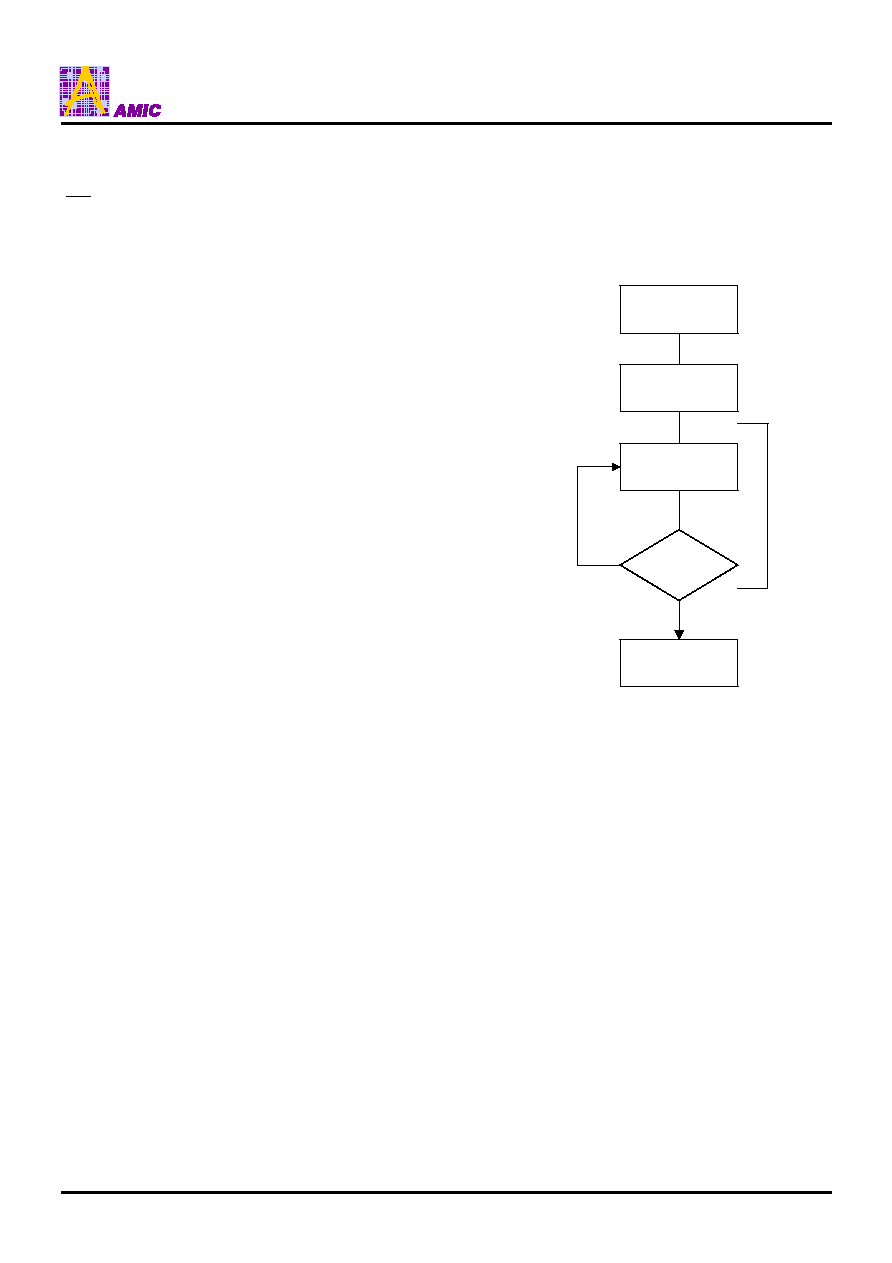
START
Write Program
Command
Sequence
Data Poll
from System
Verify Data ?
Last Address ?
Programming
Completed
No
Yes
Yes
Increment Address
Embedded
Program
algorithm in
progress
Note : See the appropriate Command Definitions table for
program command sequence.
Figure 3. Program Operation
No
Unlock Bypass Command Sequence
The unlock bypass feature allows the system to program
bytes or words to the device faster than using the standard
program command sequence. The unlock bypass command
sequence is initiated by first writing two unlock cycles. This is
followed by a third write cycle containing the unlock bypass
command, 20h. The device then enters the unlock bypass
mode. A two-cycle unlock bypass program command
sequence is all that is required to program in this mode. The
first cycle in this sequence contains the unlock bypass
program command, A0h; the second cycle contains the
program address and data. Additional data is programmed in
the same manner. This mode dispenses with the initial two
unlock cycles required in the standard program command
sequence, resulting in faster total programming time. Table 9
shows the requirements for the command sequence.
During the unlock bypass mode, only the Unlock Bypass
Program and Unlock Bypass Reset commands are valid. To
exit the unlock bypass mode, the system must issue the two-
cycle unlock bypass reset command sequence. The first
cycle must contain the data 90h; the second cycle the data
00h. Addresses are don't care for both cycle. The device
returns to reading array data.
Figure 3 illustrates the algorithm for the program operation.
See the Erase/Program Operations in "AC Characteristics" for
parameters, and to Program Operation Timings for timing
diagrams.
Chip Erase Command Sequence
Chip erase is a six-bus-cycle operation. The chip erase
command sequence is initiated by writing two unlock cycles,
followed by a set-up command. Two additional unlock write
cycles are then followed by the chip erase command, which
in turn invokes the Embedded Erase algorithm. The device
does not require the system to preprogram prior to erase. The
Embedded Erase algorithm automatically preprograms and
verifies the entire memory for an all zero data pattern prior to
electrical erase. The system is not required to provide any
controls or timings during these operations. The Command
Definitions table shows the address and data requirements
for the chip erase command sequence.
Any commands written to the chip during the Embedded
Erase algorithm are ignored. The system can determine the
status of the erase operation by using I/O
7
, I/O
6
, or I/O
2
. See
"Write Operation Status" for information on these status bits.
When the Embedded Erase algorithm is complete, the device
returns to reading array data and addresses are no longer
latched.
Figure 4 illustrates the algorithm for the erase operation. See
the Erase/Program Operations tables in "AC Characteristics"
for parameters, and to the Chip/Sector Erase Operation
Timings for timing waveforms.
Sector Erase Command Sequence
Sector erase is a six-bus-cycle operation. The sector erase
command sequence is initiated by writing two unlock cycles,
followed by a set-up command. Two additional unlock write
cycles are then followed by the address of the sector to be
erased, and the sector erase command. The Command
Definitions table shows the address and data requirements
for the sector erase command sequence.
The device does not require the system to preprogram the
memory prior to erase. The Embedded Erase algorithm
automatically programs and verifies the sector for an all zero
data pattern prior to electrical erase. The system is not
required to provide any controls or timings during these
operations.
After the command sequence is written, a sector erase time-
out of 50
�
s begins. During the time-out period, additional
sector addresses and sector erase commands may be
written. Loading the sector erase buffer may be done in any
sequence, and the number of sectors may be from one sector
to all sectors. The time between these additional cycles must
be less than 50
�
s, otherwise the last address and command
might not be accepted, and erasure may begin. It is
recommended that processor interrupts be disabled during
this time to ensure all commands are accepted. The
interrupts can be re-enabled after the last Sector Erase
command is written. If the time between additional sector
erase commands can be assumed to be less than 50
�
s, the
system need not monitor I/O
3
. Any command other than
Sector Erase or Erase Suspend during the time-out period
resets the device to reading array data. The system must
rewrite the command sequence and any additional sector
addresses and commands.
A29L160A Series
(May, 2005, Version 0.1)
16
AMIC Technology, Corp.
START
Write Erase
Command
Sequence
Data Poll
from System
Data = FFh ?
Erasure Completed
Yes
Embedded
Erase
algorithm in
progress
Note :
1. See the appropriate Command Definitions table for erase
command sequences.
2. See "I/O
3
: Sector Erase Timer" for more information.
No
Figure 4. Erase Operation
The system can monitor I/O
3
to determine if the sector erase
timer has timed out. (See the " I/O
3
: Sector Erase Timer"
section.) The time-out begins from the rising edge of the final
WE
pulse in the command sequence.
Once the sector erase operation has begun, only the Erase
Suspend command is valid. All other commands are ignored.
When the Embedded Erase algorithm is complete, the device
returns to reading array data and addresses are no longer
latched. The system can determine the status of the erase
operation by using I/O
7
, I/O
6
, or I/O
2
. Refer to "Write
Operation Status" for information on these status bits.
4 illustrates the algorithm for the erase operation. Refer to
the Erase/Program Operations tables in the "AC
Characteristics" section for parameters, and to the Sector
Erase Operations Timing diagram for timing waveforms.
Erase Suspend/Erase Resume Commands
The Erase Suspend command allows the system to interrupt
a sector erase operation and then read data from, or
program data to, any sector not selected for erasure. This
command is valid only during the sector erase operation,
including the 50
�
s time-out period during the sector erase
command sequence. The Erase Suspend command is
ignored if written during the chip erase operation or
Embedded Program algorithm. Writing the Erase Suspend
command during the Sector Erase time-out immediately
terminates the time-out period and suspends the erase
operation. Addresses are "don't cares" when writing the
Erase Suspend command.
When the Erase Suspend command is written during a
sector erase operation, the device requires a maximum of
20
�
s to suspend the erase operation. However, when the
Erase Suspend command is written during the sector erase
time-out, the device immediately terminates the time-out
period and suspends the erase operation.
After the erase operation has been suspended, the system
can read array data from or program data to any sector not
selected for erasure. (The device "erase suspends" all
sectors selected for erasure.) Normal read and write timings
and command definitions apply. Reading at any address
within erase-suspended sectors produces status data on I/O
7
- I/O
0
. The system can use I/O
7
, or I/O
6
and I/O
2
together, to
determine if a sector is actively erasing or is erase-
suspended. See "Write Operation Status" for information on
these status bits.
After an erase-suspended program operation is complete,
the system can once again read array data within non-
suspended sectors. The system can determine the status of
the program operation using the I/O
7
or I/O
6
status bits, just
as in the standard program operation. See "Write Operation
Status" for more information.
The system may also write the autoselect command
sequence when the device is in the Erase Suspend mode.
The device allows reading autoselect codes even at
addresses within erasing sectors, since the codes are not
stored in the memory array. When the device exits the
autoselect mode, the device reverts to the Erase Suspend
mode, and is ready for another valid operation. See
"Autoselect Command Sequence" for more information.
The system must write the Erase Resume command
(address bits are "don't care") to exit the erase suspend
mode and continue the sector erase operation. Further writes
of the Resume command are ignored. Another Erase
Suspend command can be written after the device has
resumed erasing.

A29L160A Series
(May, 2005, Version 0.1)
17
AMIC Technology, Corp.
Table 9. A29L160A Command Definitions
Bus Cycles (Notes 2 - 5)
First Second Third Fourth Fifth Sixth
Command
Sequence
(Note 1)
Cycle
s
Addr Data Addr Data
Addr Data Addr Data Addr Data Addr
Data
Read (Note 6)
1
RA
RD
Reset (Note 7)
1 XXX
F0
Word 555
2AA
555
Manufacturer ID
Byte
4
AAA
AA
555
55
AAA
90 X00
37
Word 555
2AA
555
X01 22C4
Device ID,
Top Boot Block
Byte
4
AAA
AA
555
55
AAA
90
X02
C4
Word 555
2AA
555
X01 2249
Device ID,
Bottom Boot Block
Byte
4
AAA
AA
555
55
AAA
90
X02
49
Word 555
2AA
555
X03
Continuation ID
Byte
4
AAA
AA
555
55
AAA
90
X06
7F
XX00
Word 555
2AA
555
(SA)
X02 XX01
00
Autoselect (Note 8) Sector Protect Verify
(Note 9)
Byte
4
AAA
AA
555
55
AAA
90
(SA)
X04
01
Word 55
CFI Query (Note 10)
Byte
1
AA
98
Byte 555
2AA
555
Program
Byte
4
AAA
AA
555
55
AAA
A0
PA
PD
Word 555
2AA
555
Unlock Bypass
Byte
3
AAA
AA
555
55
AAA
20
Unlock Bypass Program (Note
11)
2
XXX
A0
PA
PD
Unlock Bypass Reset (Note 12)
2
XXX 90
XXX
00
Word 555
2AA
555
555
2AA
555
Chip Erase
Byte
6
AAA
AA
555
55
AAA
80
AAA
AA
555
55
AAA
10
Word 555
2AA
555
555
2AA
Sector Erase
Byte
6
AAA
AA
555
55
AAA
80
AAA
AA
555
55 SA 30
Erase Suspend (Note 13)
1 XXX
B0
Erase Resume (Note 14)
1 XXX
30
Legend:
X = Don't care
RA = Address of the memory location to be read.
RD = Data read from location RA during read operation.
PA = Address of the memory location to be programmed. Addresses latch on the falling edge of the
WE
or
CE
pulse,
whichever happens later.
PD = Data to be programmed at location PA. Data latches on the rising edge of
WE
or
CE
pulse, whichever happens first.
SA = Address of the sector to be verified (in autoselect mode) or erased. Address bits A19 - A12 select a unique sector.
Note:
1. See Table 1 for description of bus operations.
2. All values are in hexadecimal.
3. Except when reading array or autoselect data, all bus cycles are write operation.
4. Address bits A19 - A11 are don't cares for unlock and command cycles, unless SA or PA required.
5. No unlock or command cycles required when reading array data.
6. The Reset command is required to return to reading array data when device is in the autoselect mode, or if I/O
5
goes high
(while the device is providing status data).
7. The fourth cycle of the autoselect command sequence is a read cycle.
8. The data is 00h for an unprotected sector and 01h for a protected sector. See "Autoselect Command Sequence" for more
information.
9. The data is 00h for an unprotected sector and 01h for a protected sector. See "Autoselect Command Sequence" for more
information.
10. Command is valid when device is ready to read array data or when device is in autoselect mode.
11. The Unlock Bypass command is required prior to the Unlock Bypass Program command.
12. The Unlock Bypass Reset command is required to return to reading array data when the device is in the unlock bypass
mode.
13. The system may read and program in non-erasing sectors, or enter the autoselect mode, when in the Erase Suspend mode.
14. The Erase Resume command is valid only during the Erase Suspend mode.
A29L160A Series
(May, 2005, Version 0.1)
18
AMIC Technology, Corp.
Write Operation Status
Several bits, I/O
2
, I/O
3
, I/O
5
, I/O
6
, I/O
7,
RY/
BY
are provided in
the A29L160A to determine the status of a write operation.
Table 10 and the following subsections describe the
functions of these status bits. I/O
7
, I/O
6
and RY/
BY
each
offer a method for determining whether a program or erase
operation is complete or in progress. These three bits are
discussed first.
I/O
7
:
Data
Polling
The
Data
Polling bit, I/O
7
, indicates to the host system
whether an Embedded Algorithm is in progress or completed,
or whether the device is in Erase Suspend.
Data
Polling is
valid after the rising edge of the final
WE
pulse in the
program or erase command sequence.
During the Embedded Program algorithm, the device outputs
on I/O
7
the complement of the datum programmed to I/O
7
.
This I/O
7
status also applies to programming during Erase
Suspend. When the Embedded Program algorithm is
complete, the device outputs the datum programmed to I/O
7
.
The system must provide the program address to read valid
status information on I/O
7
. If a program address falls within a
protected sector,
Data
Polling on I/O
7
is active for
approximately 2
�
s, then the device returns to reading array
data.
During the Embedded Erase algorithm,
Data
Polling
produces a "0" on I/O
7
. When the Embedded Erase algorithm
is complete, or if the device enters the Erase Suspend mode,
Data
Polling produces a "1" on I/O
7
.This is analogous to the
complement/true datum output described for the Embedded
Program algorithm: the erase function changes all the bits in
a sector to "1"; prior to this, the device outputs the
"complement," or "0." The system must provide an address
within any of the sectors selected for erasure to read valid
status information on I/O
7
.
After an erase command sequence is written, if all sectors
selected for erasing are protected,
Data
Polling on I/O
7
is
active for approximately 100
�
s, then the device returns to
reading array data. If not all selected sectors are protected,
the Embedded Erase algorithm erases the unprotected
sectors, and ignores the selected sectors that are protected.
When the system detects I/O
7
has changed from the
complement to true data, it can read valid data at I/O
7
- I/O
0
on the following read cycles. This is because I/O
7
may
change asynchronously with I/O
0
- I/O
6
while Output Enable
(
OE
) is asserted low. The
Data
Polling Timings (During
Embedded Algorithms) figure in the "AC Characteristics"
section illustrates this. Table 10 shows the outputs for
Data
Polling on I/O
7
. Figure 5 shows the
Data
Polling algorithm.
START
Read I/O
7
-I/O
0
Address = VA
I/O
7
= Data ?
FAIL
No
Note :
1. VA = Valid address for programming. During a sector
erase operation, a valid address is an address within any
sector selected for erasure. During chip erase, a valid
address is any non-protected sector address.
2. I/O
7
should be rechecked even if I/O
5
= "1" because
I/O
7
may change simultaneously with I/O
5
.
No
Read I/O
7
- I/O
0
Address = VA
I/O
5
= 1?
I/O
7
= Data ?
Yes
No
PASS
Yes
Yes
Figure 5. Data Polling Algorithm

A29L160A Series
(May, 2005, Version 0.1)
19
AMIC Technology, Corp.
RY/
BY
: Read/
Busy
The RY/
BY
is a dedicated, open-drain output pin that
indicates whether an Embedded algorithm is in progress or
complete. The RY/
BY
status is valid after the rising edge of
the final
WE
pulse in the command sequence. Since RY/
BY
is an open-drain output, several RY/
BY
pins can be tied
together in parallel with a pull-up resistor to VCC. (The
RY/
BY
pin is not available on the 44-pin SOP package)
If the output is low (Busy), the device is actively erasing or
programming. (This includes programming in the Erase
Suspend mode.) If the output is high (Ready), the device is
ready to read array data (including during the Erase Suspend
mode), or is in the standby mode.
Table 10 shows the outputs for RY/
BY
. Refer to "
RESET
Timings", "Timing Waveforms for Program Operation" and
"Timing Waveforms for Chip/Sector Erase Operation" for
more information.
I/O
6
: Toggle Bit I
Toggle Bit I on I/O
6
indicates whether an Embedded Program
or Erase algorithm is in progress or complete, or whether the
device has entered the Erase Suspend mode. Toggle Bit I
may be read at any address, and is valid after the rising edge
of the final
WE
pulse in the command sequence (prior to the
program or erase operation), and during the sector erase
time-out.
During an Embedded Program or Erase algorithm operation,
successive read cycles to any address cause I/O
6
to toggle.
(The system may use either
OE
or
CE
to control the read
cycles.) When the operation is complete, I/O
6
stops toggling.
After an erase command sequence is written, if all sectors
selected for erasing are protected, I/O
6
toggles for
approximately 100
�
s, then returns to reading array data. If not
all selected sectors are protected, the Embedded Erase
algorithm erases the unprotected sectors, and ignores the
selected sectors that are protected.
The system can use I/O
6
and I/O
2
together to determine
whether a sector is actively erasing or is erase-suspended.
When the device is actively erasing (that is, the Embedded
Erase algorithm is in progress), I/O
6
toggles. When the device
enters the Erase Suspend mode, I/O
6
stops toggling.
However, the system must also use I/O
2
to determine which
sectors are erasing or erase-suspended. Alternatively, the
system can use I/O
7
(see the subsection on " I/O
7
:
Data
Polling").
If a program address falls within a protected sector, I/O
6
toggles for approximately 2
�
s after the program command
sequence is written, then returns to reading array data.
I/O
6
also toggles during the erase-suspend-program mode,
and stops toggling once the Embedded Program algorithm is
complete.
The Write Operation Status table shows the outputs for
Toggle Bit I on I/O
6
. Refer to Figure 6 for the toggle bit
algorithm, and to the Toggle Bit Timings figure in the "AC
Characteristics" section for the timing diagram. The I/O
2
vs.
I/O
6
figure shows the differences between I/O
2
and I/O
6
in
graphical form. See also the subsection on " I/O
2
: Toggle Bit
II".
I/O
2
: Toggle Bit II
The "Toggle Bit II" on I/O
2
, when used with I/O
6
, indicates
whether a particular sector is actively erasing (that is, the
Embedded Erase algorithm is in progress), or whether that
sector is erase-suspended. Toggle Bit II is valid after the
rising edge of the final
WE
pulse in the command sequence.
I/O
2
toggles when the system reads at addresses within those
sectors that have been selected for erasure. (The system may
use either
OE
or
CE
to control the read cycles.) But I/O
2
cannot distinguish whether the sector is actively erasing or is
erase-suspended. I/O
6
, by comparison, indicates whether the
device is actively erasing, or is in Erase Suspend, but cannot
distinguish which sectors are selected for erasure. Thus, both
status bits are required for sector and mode information.
Refer to Table 10 to compare outputs for I/O
2
and I/O
6
.
Figure 6 shows the toggle bit algorithm in flowchart form, and
the section " I/O
2
: Toggle Bit II" explains the algorithm. See
also the " I/O
6
: Toggle Bit I" subsection. Refer to the Toggle
Bit Timings figure for the toggle bit timing diagram. The I/O
2
vs. I/O
6
figure shows the differences between I/O
2
and I/O
6
in
graphical form.
Reading Toggle Bits I/O
6
, I/O
2
Refer to Figure 6 for the following discussion. Whenever the
system initially begins reading toggle bit status, it must read
I/O
7
- I/O
0
at least twice in a row to determine whether a
toggle bit is toggling. Typically, a system would note and store
the value of the toggle bit after the first read. After the second
read, the system would compare the new value of the toggle
bit with the first. If the toggle bit is not toggling, the device has
completed the program or erase operation. The system can
read array data on I/O
7
- I/O
0
on the following read cycle.
However, if after the initial two read cycles, the system
determines that the toggle bit is still toggling, the system also
should note whether the value of I/O
5
is high (see the section
on I/O
5
). If it is, the system should then determine again
whether the toggle bit is toggling, since the toggle bit may
have stopped toggling just as I/O
5
went high. If the toggle bit
is no longer toggling, the device has successfully completed
the program or erase operation. If it is still toggling, the device
did not complete the operation successfully, and the system
must write the reset command to return to reading array data.
The remaining scenario is that the system initially determines
that the toggle bit is toggling and I/O
5
has not gone high. The
system may continue to monitor the toggle bit and I/O
5
through successive read cycles, determining the status as
described in the previous paragraph. Alternatively, it may
choose to perform other system tasks. In this case, the
system must start at the beginning of the algorithm when it
returns to determine the status of the operation (top of Figure
6).
I/O
5
: Exceeded Timing Limits
I/O
5
indicates whether the program or erase time has
exceeded a specified internal pulse count limit. Under these
conditions I/O
5
produces a "1." This is a failure condition that
indicates the program or erase cycle was not successfully
completed.
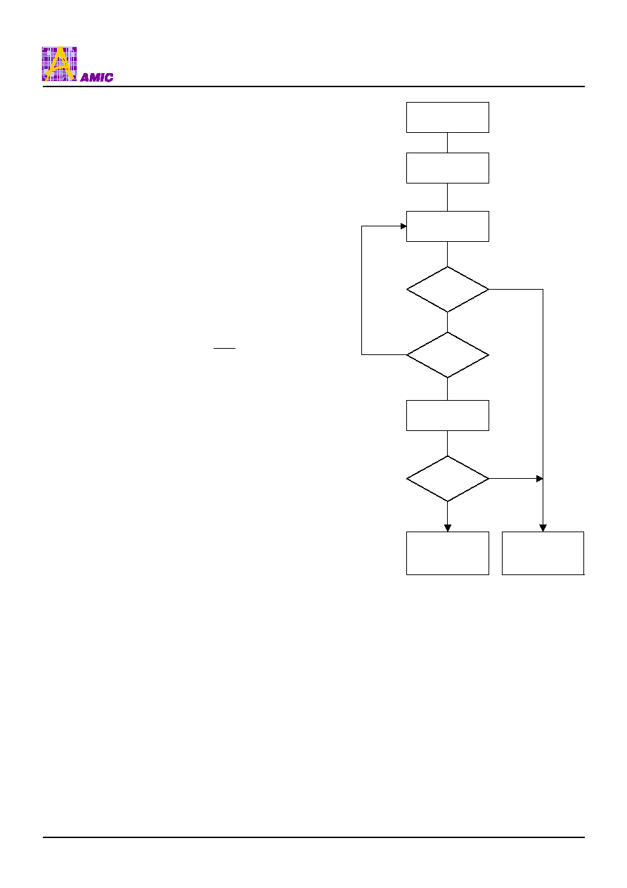
A29L160A Series
(May, 2005, Version 0.1)
20
AMIC Technology, Corp.
The I/O
5
failure condition may appear if the system tries to
program a "1 "to a location that is previously programmed to
"0." Only an erase operation can change a "0" back to a "1."
Under this condition, the device halts the operation, and
when the operation has exceeded the timing limits, I/O
5
produces a "1."
Under both these conditions, the system must issue the reset
command to return the device to reading array data.
I/O
3
: Sector Erase Timer
After writing a sector erase command sequence, the system
may read I/O
3
to determine whether or not an erase
operation has begun. (The sector erase timer does not apply
to the chip erase command.) If additional sectors are
selected for erasure, the entire time-out also applies after
each additional sector erase command. When the time-out is
complete, I/O
3
switches from "0" to "1." The system may
ignore I/O
3
if the system can guarantee that the time
between additional sector erase commands will always be
less than 50
�
s. See also the "Sector Erase Command
Sequence" section.
After the sector erase command sequence is written, the
system should read the status on I/O
7
(
Data
Polling) or I/O
6
(Toggle Bit 1) to ensure the device has accepted the
command sequence, and then read I/O
3
. If I/O
3
is "1", the
internally controlled erase cycle has begun; all further
commands (other than Erase Suspend) are ignored until the
erase operation is complete. If I/O
3
is "0", the device will
accept additional sector erase commands. To ensure the
command has been accepted, the system software should
check the status of I/O
3
prior to and following each
subsequent sector erase command. If I/O
3
is high on the
second status check, the last command might not have been
accepted. Table 10 shows the outputs for I/O
3
.
START
Read I/O
7
-I/O
0
Toggle Bit
= Toggle ?
Program/Erase
Operation Not
Commplete, Write
Reset Command
Yes
Notes :
1. Read toggle bit twice to determine whether or not it is
toggling. See text.
2. Recheck toggle bit because it may stop toggling as I/O
5
changes to "1". See text.
No
Read I/O
7
- I/O
0
Twice
I/O
5
= 1?
Toggle Bit
= Toggle ?
Yes
Yes
Program/Erase
Operation Complete
No
No
Read I/O
7
-I/O
0
(Notes 1,2)
Figure 6. Toggle Bit Algorithm
(Note 1)
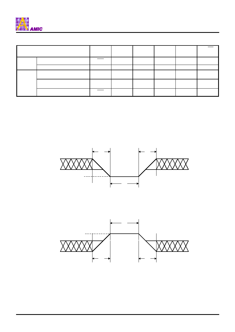
A29L160A Series
(May, 2005, Version 0.1)
21
AMIC Technology, Corp.
Table 10. Write Operation Status
I/O
7
I/O
6
I/O
5
I/O
3
I/O
2
RY/
BY
Operation
(Note
1) (Note
2) (Note
1)
Embedded Program Algorithm
7
I/O
Toggle 0 N/A
No
toggle
0
Standard
Mode
Embedded Erase Algorithm
0
Toggle
0
1
Toggle
0
Reading within Erase
Suspended Sector
1 No
toggle
0
N/A Toggle 1
Reading within Non-Erase
Suspend Sector
Data Data Data Data Data 1
Erase
Suspend
Mode
Erase-Suspend-Program
7
I/O
Toggle 0 N/A N/A 0
Notes:
1. I/O
7
and I/O
2
require a valid address when reading status information. Refer to the appropriate subsection for further details.
2. I/O
5
switches to "1" when an Embedded Program or Embedded Erase operation has exceeded the maximum timing limits.
See "I/O5: Exceeded Timing Limits" for more information.
Maximum Negative Input Overshoot
20ns
20ns
20ns
+0.8V
-0.5V
-2.0V
Maximum Positive Input Overshoot
20ns
20ns
20ns
VCC+0.5V
2.0V
VCC+2.0V

A29L160A Series
(May, 2005, Version 0.1)
22
AMIC Technology, Corp.
DC Characteristics
CMOS Compatible
Parameter
Symbol
Parameter Description
Test Description
Min.
Typ.
Max.
Unit
I
LI
Input Load Current
V
IN
= VSS to VCC. VCC = VCC Max
�
1.0
�
A
I
LIT
A9 Input Load Current
VCC = VCC Max, A9 =12.5V
35
�
A
I
LO
Output Leakage Current
V
OUT
= VSS to VCC. VCC = VCC Max
�
1.0
�
A
5 MHz
9 16
CE
= V
IL
,
OE
= V
IH
Byte Mode
1 MHz
2 4
5 MHz
9
16
I
CC1
VCC Active Read Current
(Notes 1, 2)
CE
= V
IL
,
OE
= V
IH
Word Mode
1 MHz
2
4
mA
I
CC2
VCC Active Write (Program/Erase)
Current (Notes 2, 3, 4)
CE
= V
IL
,
OE
=V
IH
20
30 mA
I
CC3
VCC Standby Current (Note 2)
CE
= V
IH
,
RESET
= VCC
�
0.3V
0.2
5
�
A
I
CC4
VCC Standby Current During Reset
(Note 2)
RESET
= VSS
�
0.3V
0.2 5
�
A
I
CC5
Automatic Sleep Mode
(Note 2, 4, 5)
V
IH
= VCC
�
0.3V; V
IL
= VSS
�
0.3V
0.2 5
�
A
V
IL
Input Low Level
-0.5
0.8
V
V
IH
Input High Level
0.7 x VCC
VCC + 0.3
V
V
ID
Voltage for Autoselect and
Temporary Unprotect Sector
VCC = 3.3 V
11.5
12.5
V
V
OL
Output Low Voltage
I
OL
= 4.0mA, VCC = VCC Min
0.45
V
V
OH1
I
OH
= -2.0 mA, VCC = VCC Min
0.85 x VCC
V
V
OH2
Output High Voltage
I
OH
= -100
�
A, VCC = VCC Min
VCC - 0.4
V
Notes:
1. The I
CC
current listed is typically less than 2 mA/MHz, with
OE
at V
IH
. Typical VCC is 3.3V.
2. Maximum I
CC
specifications are tested with VCC = VCC max.
3. I
CC
active while Embedded Algorithm (program or erase) is in progress.
4. Automatic sleep mode enables the low power mode when addresses remain stable for t
ACC
+ 30ns. Typical sleep mode current
is 200nA.
5. Not 100% tested.

A29L160A Series
(May, 2005, Version 0.1)
23
AMIC Technology, Corp.
DC Characteristics (continued)
Zero Power Flash
0
500
1000
1500
2000
2500
3000
3500
4000
5
0
10
15
20
25
Time in ns
Supply Current in mA
Note: Addresses are switching at 1MHz
I
CC1
Current vs. Time (Showing Active and Automatic Sleep Currents)
1
2
3
4
5
0
2
4
6
8
10
Frequency in MHz
Su
p
p
ly
Cu
rrent
in mA
C
25
T
:
Note
�
=
Typical I
CC1
vs. Frequency
3.6V
3.0V
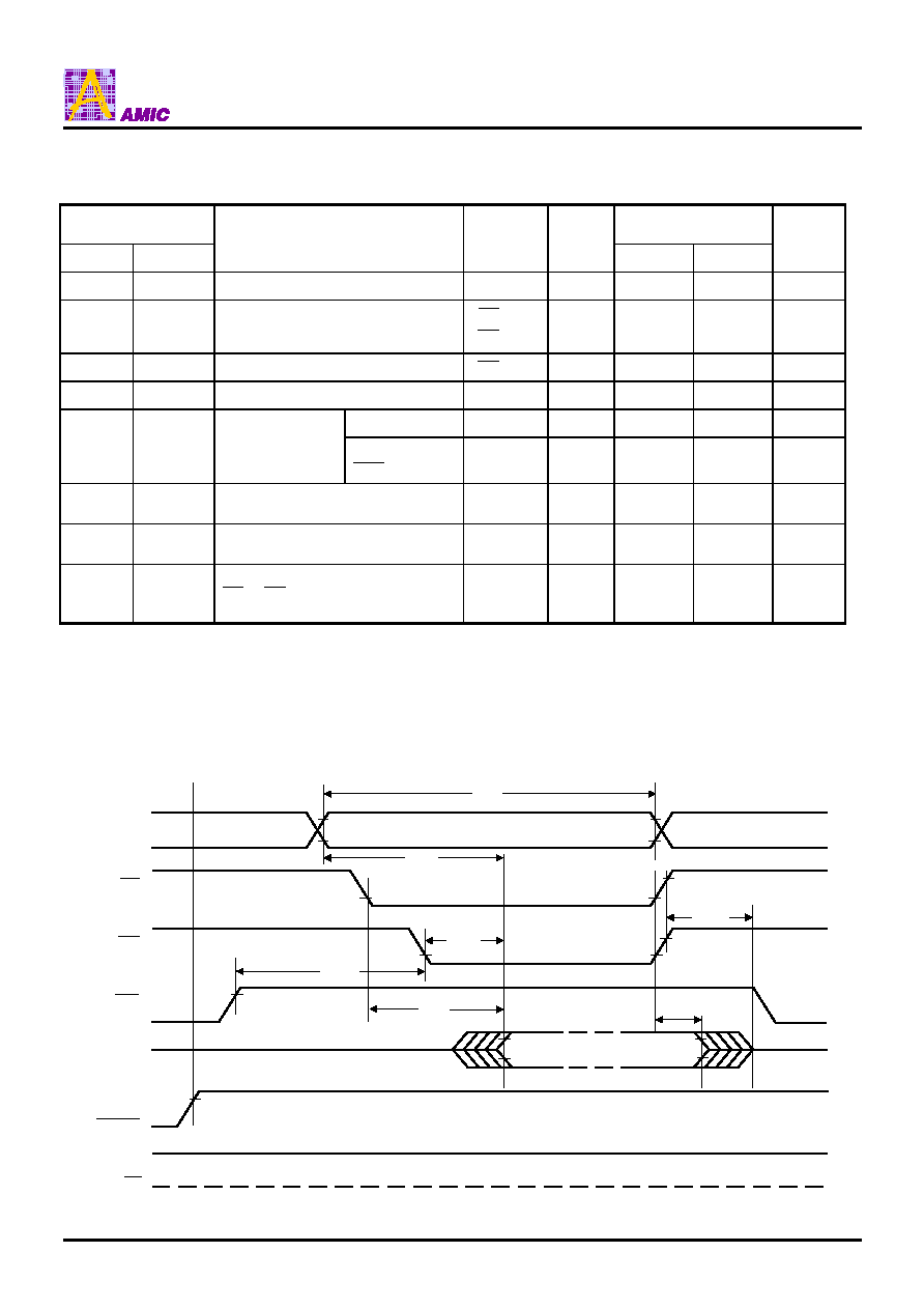
A29L160A Series
(May, 2005, Version 0.1)
24
AMIC Technology, Corp.
AC Characteristics
Read Only Operations
Parameter Symbols
Speed
JEDEC
Std
Description Test
Setup
-70
-90
Unit
t
AVAV
t
RC
Read Cycle Time (Note 1)
Min.
70
90
ns
t
AVQV
t
ACC
Address to Output Delay
CE
= V
IL
OE
= V
IL
Max.
70
90
ns
t
ELQV
t
CE
Chip Enable to Output Delay
OE
= V
IL
Max.
70
90
ns
t
GLQV
t
OE
Output Enable to Output Delay
Max.
30
35
ns
Read
Min.
0
0
ns
t
OEH
Output Enable Hold
Time (Note 1)
Toggle and
Data
Polling
Min. 10 10
ns
t
EHQZ
t
HZ
Chip Enable to Output High Z
(Notes 1)
Max. 25 30 ns
t
GHQZ
t
DF
Output Enable to Output High Z
(Notes 1)
25 30 ns
t
AXQX
t
OH
Output Hold Time from Addresses,
CE
or
OE
, Whichever Occurs First
(Note 1)
Min. 0
0 ns
Notes:
1. Not 100% tested.
2. See Test Conditions and Test Setup for test specifications.
Timing Waveforms for Read Only Operation
Addresses
Addresses Stable
CE
OE
WE
Output Valid
High-Z
Output
t
RC
t
OEH
t
OE
t
CE
High-Z
t
OH
t
DF
t
ACC
0V
RESET
RY/BY
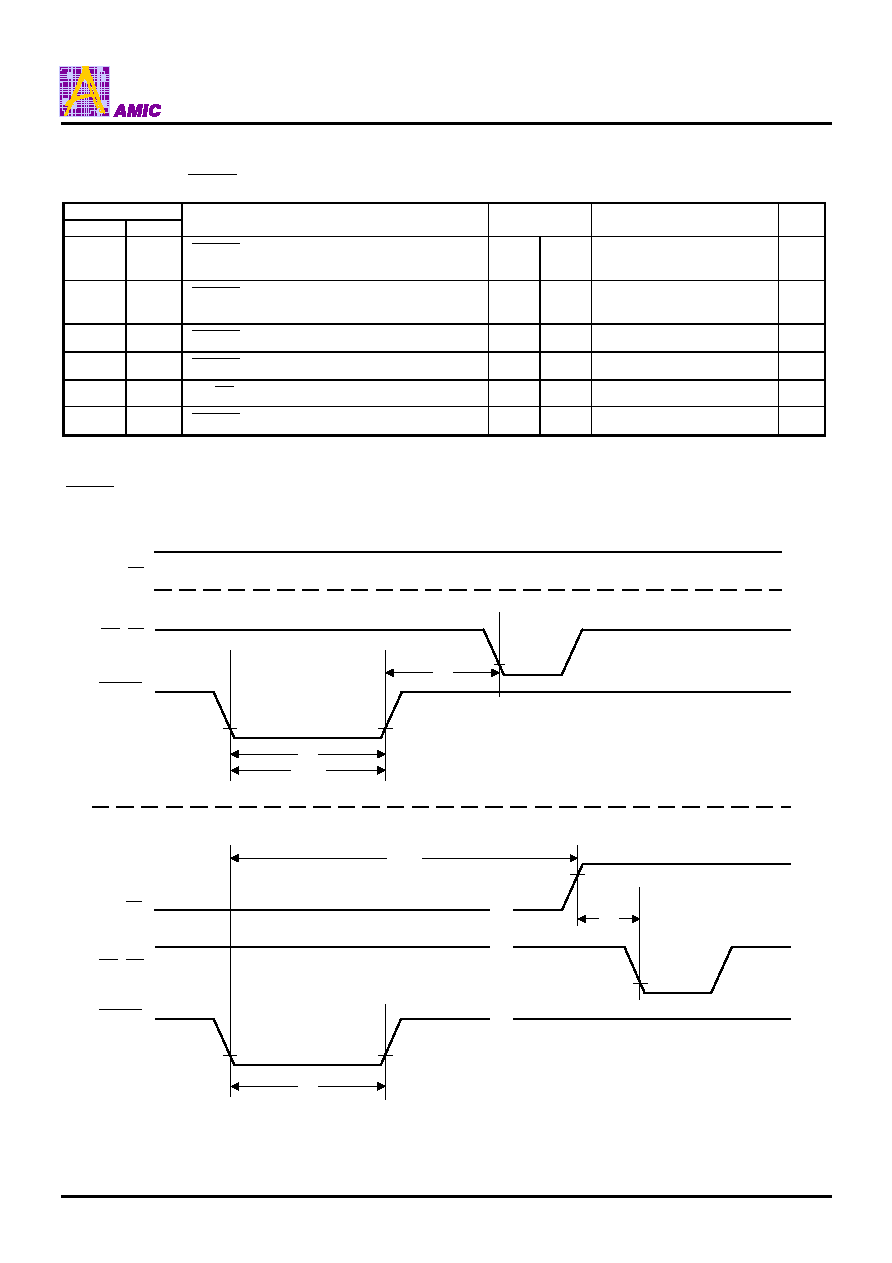
A29L160A Series
(May, 2005, Version 0.1)
25
AMIC Technology, Corp.
AC Characteristics
Hardware Reset (
RESET
)
Parameter
JEDEC Std
Description
Test Setup
All Speed Options
Unit
t
READY
RESET
Pin Low (During Embedded
Algorithms) to Read or Write (See Note)
Max
20
�
s
t
READY
RESET
Pin Low (Not During Embedded
Algorithms) to Read or Write (See Note)
Max
500 ns
t
RP
RESET
Pulse Width
Min
500
ns
t
RH
RESET
High Time Before Read (See Note)
Min
50
ns
t
RB
RY/
BY
Recovery Time
Min
0
ns
t
RPD
RESET
Low to Standby Mode
Min
20
�
s
Note: Not 100% tested.
RESET
Timings
CE, OE
RESET
t
RH
t
RP
t
Ready
Reset Timings NOT during Embedded Algorithms
RESET
t
RP
~~
Reset Timings during Embedded Algorithms
RY/BY
~ ~
t
RB
~ ~
t
Ready
CE, OE
RY/BY

A29L160A Series
(May, 2005, Version 0.1)
26
AMIC Technology, Corp.
Temporary Sector Unprotect
Parameter
JEDEC Std
Description
All Speed Options
Unit
t
VIDR
V
ID
Rise and Fall Time (See Note)
Min
500
ns
t
RSP
RESET
Setup Time for Temporary Sector
Unprotect
Min 4
�
s
Note: Not 100% tested.
Temporary Sector Unprotect Timing Diagram
AC Characteristics
Word/Byte Configuration (
BYTE
)
Parameter
All Speed Options
JEDEC Std
Description
-70 -90
Unit
t
ELFL/
t
ELFH
CE
to
BYTE
Switching Low or High
Max 5 ns
t
FLQZ
BYTE
Switching Low to Output High-Z
Max 25 30 ns
t
HQV
BYTE
Switching High to Output Active
Min 70 90 ns
Program or Erase Command Sequence
RESET
~~
~~
~~
12V
0 or 3V
t
VIDR
t
VIDR
0 or 3V
t
RSP
CE
WE
RY/BY
~~
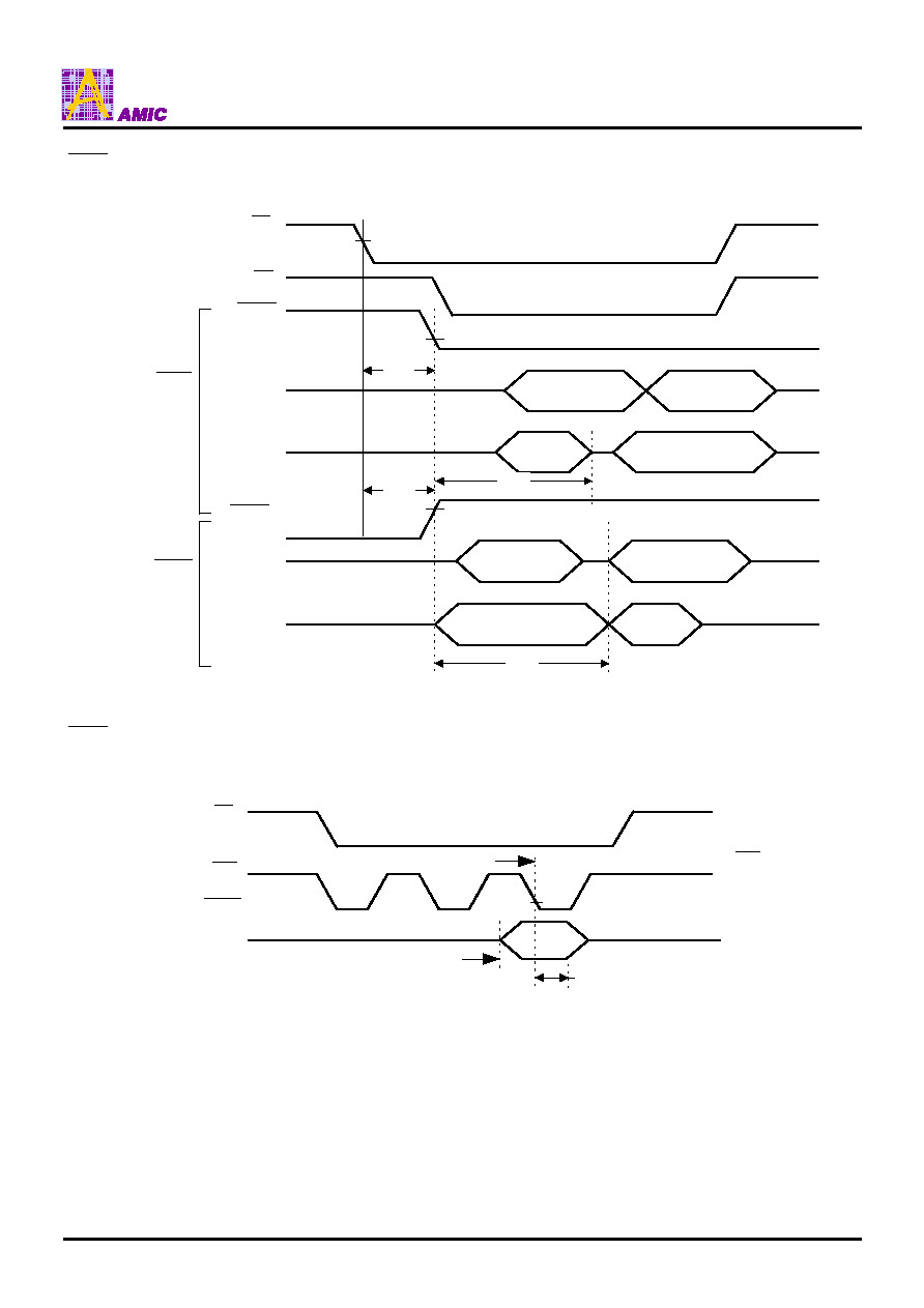
A29L160A Series
(May, 2005, Version 0.1)
27
AMIC Technology, Corp.
Data Output
(I/O
0
-I/O
14
)
Data Output
(I/O
0
-I/O
7
)
I/O
15
Output
Address Input
Data Output
(I/O
0
-I/O
14
)
Data Output
(I/O
0
-I/O
7
)
I/O
15
Output
Address Input
t
FHQV
t
FLQZ
t
ELFH
t
ELFL
CE
OE
BYTE
I/O
0
-I/O
14
I/O
15
(A-1)
BYTE
I/O
0
-I/O
14
I/O
15
(A-1)
BYTE
Switching
from word to
byte mode
BYTE
Switching
from byte to
word mode
BYTE
Timings for Read Operations
BYTE
Timings for Write Operations
Note:
Refer to the Erase/Program Operations table for t
AS
and t
AH
specifications.
The falling edge of the last WE signal
t
HOLD
(t
AH
)
t
SET
(t
AS
)
CE
BYTE
WE

A29L160A Series
(May, 2005, Version 0.1)
28
AMIC Technology, Corp.
AC Characteristics
Erase and Program Operations
Parameter
Speed
JEDEC
Std
Description
-70
-90
Unit
t
AVAV
t
WC
Write Cycle Time (Note 1)
Min.
70
90
ns
t
AVWL
t
AS
Address Setup Time
Min.
0
ns
t
WLAX
t
AH
Address Hold Time
Min.
45
45
ns
t
DVWH
t
DS
Data Setup Time
Min.
35
45
ns
t
WHDX
t
DH
Data Hold Time
Min.
0
ns
t
OES
Output Enable Setup Time
Min.
0
ns
t
GHWL
t
GHWL
Read Recover Time Before Write
(
OE
high to
WE
low)
Min.
0
ns
t
ELWL
t
CS
CE
Setup Time
Min.
0
ns
t
WHEH
t
CH
CE
Hold Time
Min.
0
ns
t
WLWH
t
WP
Write Pulse Width
Min.
35
35
ns
t
WHWL
t
WPH
Write Pulse Width High
Min.
30
ns
Byte Typ.
20
t
WHWH1
t
WHWH1
Byte Programming Operation
(Note 2)
Word Typ.
40
�
s
t
WHWH2
t
WHWH2
Sector
Erase
Operation
(Note 2)
Typ.
1.0
sec
t
vcs
VCC Set Up Time (Note 1)
Min.
50
�
s
t
RB
Recovery Time from RY/
BY
(Note 1)
Min
0
ns
t
BUSY
Program/Erase Valid to RY/
BY
Delay (Note 1)
Min
90
ns
Notes:
1. Not 100% tested.
2. See the "Erase and Programming Performance" section for more information.
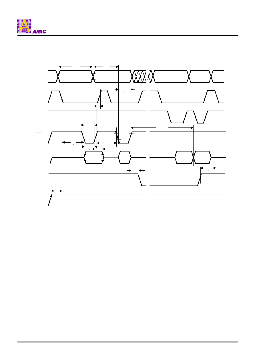
A29L160A Series
(May, 2005, Version 0.1)
29
AMIC Technology, Corp.
Timing Waveforms for Program Operation
Addresses
CE
OE
WE
Data
VCC
A0h
PD
t
WC
PA
Program Command Sequence (last two cycles)
PA
D
OUT
~ ~
~ ~
PA
~ ~
Status
~ ~
~ ~
~ ~
~ ~
t
AS
t
VCS
Read Status Data (last two cycles)
555h
t
AH
t
WHWH1
t
CH
t
WP
t
WPH
t
CS
t
DS
t
DH
Note :
1. PA = program addrss, PD = program data, Dout is the true data at the program address.
2. Illustration shows device in word mode.
~ ~
t
RB
t
BUSY
RY/BY
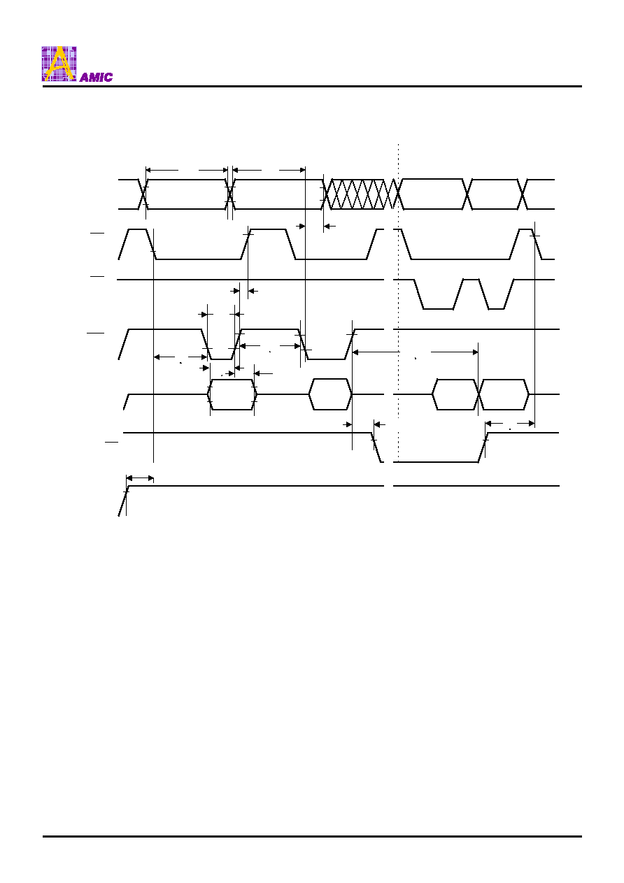
A29L160A Series
(May, 2005, Version 0.1)
30
AMIC Technology, Corp.
Addresses
CE
OE
WE
Data
VCC
55h
30h
t
WC
SA
Erase Command Sequence (last two cycles)
VA
Complete
~ ~
~ ~
VA
~ ~
In
Progress
~ ~
~ ~
~ ~
~ ~
t
AS
t
VCS
Read Status Data
2AAh
t
AH
t
WHWH2
t
CH
t
WP
t
WPH
t
CS
t
DS
t
DH
Note :
1. SA = Sector Address (for Sector Erase), VA = Valid Address for reading status data (see "Write Operaion Ststus").
2. Illustratin shows device in word mode.
555h for chip erase
10h for chip erase
~ ~
t
RB
t
BUSY
RY/BY
Timing Waveforms for Chip/Sector Erase Operation

A29L160A Series
(May, 2005, Version 0.1)
31
AMIC Technology, Corp.
Timing Waveforms for
Data
Polling (During Embedded Algorithms)
Addresses
CE
OE
WE
I/O
7
t
RC
VA
VA
VA
~ ~
~ ~
~ ~
~ ~
~ ~
Complement
~ ~
Complement
True
Valid Data
High-Z
Status Data
~ ~
Status Data
True
Valid Data
High-Z
I/O
0
- I/O
6
t
ACC
t
CE
t
CH
t
OE
t
OEH
t
DF
t
OH
Note : VA = Valid Address. Illustation shows first status cycle after command sequence, last status read cycle, and array data
read cycle.
~ ~
t
BUSY
RY/BY
High-Z
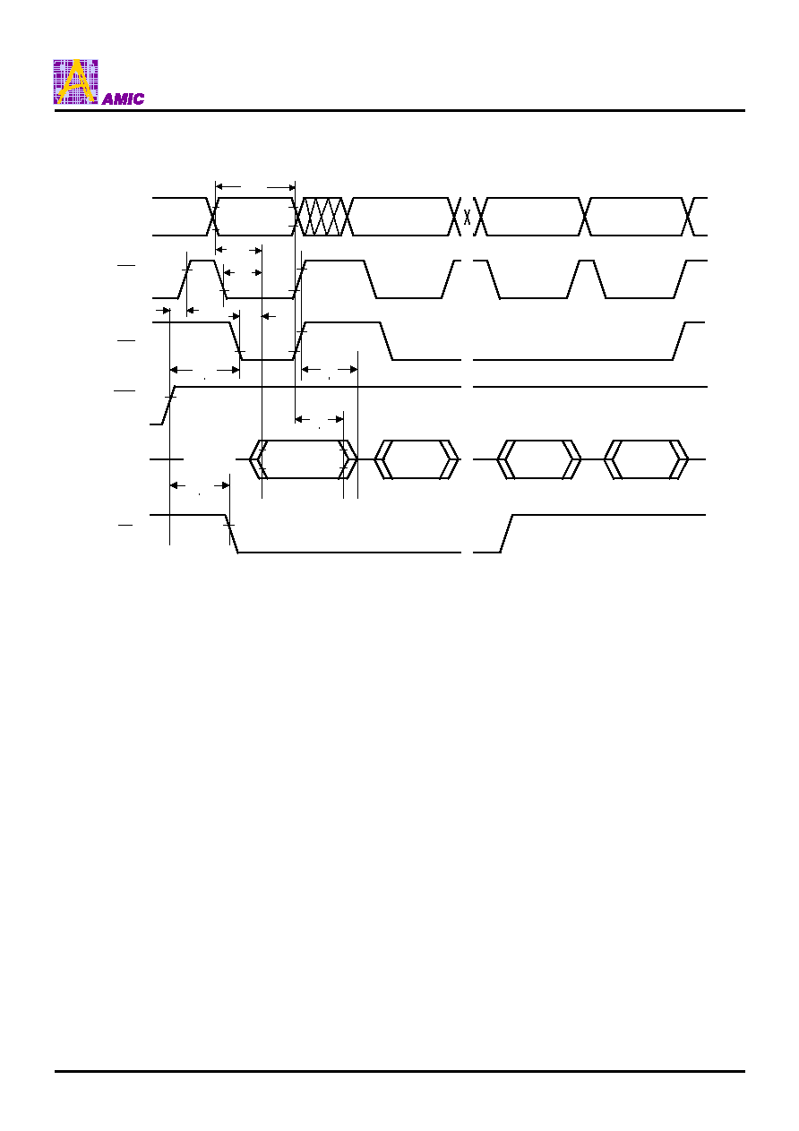
A29L160A Series
(May, 2005, Version 0.1)
32
AMIC Technology, Corp.
Timing Waveforms for Toggle Bit (During Embedded Algorithms)
Note: VA = Valid Address; not required for I/O
6
. Illustration shows first two status cycle after command sequence, last status
read cycle, and array data read cycle.
Addresses
CE
OE
WE
I/O
6
, I/O
2
t
RC
VA
VA
VA
~ ~
~ ~
~ ~
~ ~
~ ~
Valid Status
t
ACC
t
CE
t
CH
t
OE
t
OEH
t
DF
t
OH
VA
Valid Status
Valid Status
Valid Data
~ ~
(first read)
(second read)
(stop togging)
RY/BY
~ ~
t
BUSY
High-Z

A29L160A Series
(May, 2005, Version 0.1)
33
AMIC Technology, Corp.
Timing Waveforms for Sector Protect/Unprotect
V
ID
Note : For sector protect, A6=0, A1=1, A0=0. For sector unprotect, A6=1, A1=1, A0=0
~ ~
~ ~
~ ~
~ ~
V
IH
RESET
SA, A6,
A1, A0
Data
CE
WE
OE
Valid*
Valid*
Valid*
60h
60h
40h
Status
Sector Protect/Unprotect
Verify
1us
Sector Protect:150us
Sector Unprotect:15ms
Timing Waveforms for I/O
2
vs. I/O
6
Enter
Embedded
Erasing
Erase
Suspend
Enter Erase
Suspend Program
Erase
Resume
WE
I/O
6
I/O
2
Erase
Erase Suspend
Read
Erase Suspend
Read
Erase
Erase
Complete
I/O
2
and I/O
6
toggle with OE and CE
Note : Both I/O
6
and I/O
2
toggle with OE or CE. See the text on I/O
6
and I/O
2
in the section "Write Operation Status" for
more information.
~ ~
~ ~
~ ~
Erase
Suspend
Program
~ ~
~ ~
~ ~
~ ~
~ ~
~ ~
~ ~
~ ~
~ ~
~ ~
~ ~
~ ~

A29L160A Series
(May, 2005, Version 0.1)
34
AMIC Technology, Corp.
Timing Waveforms for Alternate
CE
Controlled Write Operation
Addresses
WE
OE
CE
Data
555 for program
2AA for erase
PA
D
OUT
~ ~
~ ~
I/O
7
~ ~
~ ~
~ ~
Data Polling
Note :
1. PA = Program Address, PD = Program Data, SA = Sector Address, I/O
7
= Complement of Data Input, D
OUT
= Array Data.
2. Figure indicates the last two bus cycles of the command sequence.
PD for program
30 for sector erase
10 for chip erase
~ ~
t
BUSY
t
WHWH1 or 2
t
AH
t
AS
t
WC
t
WH
t
CP
t
WS
t
CPH
PA for program
SA for sector erase
555 for chip erase
A0 for program
55 for erase
t
RH
t
DS
t
DH
~ ~
~ ~
RESET
RY/BY
Erase and Programming Performance
Parameter
Typ. (Note 1)
Max. (Note 2)
Unit
Comments
Sector Erase Time
1.0
8
sec
Chip Erase Time
35
sec
Excludes 00h programming
prior to erasure
Byte Programming Time
20
300
�
s
Word Programming Time
40
500
�
s
Byte Mode
22
33
sec
Chip Programming Time
(Note 3)
Word Mode
15
22
sec
Excludes system-level
overhead (Note 5)
Notes:
1. Typical program and erase times assume the following conditions: 25
�
C, 3.0V VCC, 10,000 cycles. Additionally, programming
typically assumes checkerboard pattern.
2. Under worst case conditions of 90
�
C, VCC = 3.0V, 100,000 cycles.
3. The typical chip programming time is considerably less than the maximum chip programming time listed, since most bytes
program faster than the maximum byte program time listed. If the maximum byte program time given is exceeded, only then
does the device set I/O
5
= 1. See the section on I/O
5
for further information.
4. In the pre-programming step of the Embedded Erase algorithm, all bytes are programmed to 00h before erasure.
5. System-level overhead is the time required to execute the four-bus-cycle command sequence for programming. See Table 9
for further information on command definitions.
6. The device has a guaranteed minimum erase and program cycle endurance of 10,000 cycles.
A29L160A Series
(May, 2005, Version 0.1)
35
AMIC Technology, Corp.
Latch-up Characteristics
Description Min.
Max.
Input Voltage with respect to VSS on all I/O pins
-1.0V
VCC+1.0V
VCC Current
-100 mA
+100 mA
Input voltage with respect to VSS on all pins except I/O pins
(including A9,
OE
and
RESET
)
-1.0V
12.5V
Includes all pins except VCC. Test conditions: VCC = 5.0V, one pin at time.
TSOP and SOP Pin Capacitance
Parameter Symbol
Parameter Description
Test Setup
Typ.
Max.
Unit
C
IN
Input
Capacitance
V
IN
=0
6
7.5
pF
C
OUT
Output Capacitance
V
OUT
=0
8.5
12
pF
C
IN2
Control Pin Capacitance
V
IN
=0
7.5
9
pF
Notes:
1. Sampled, not 100% tested.
2. Test conditions T
A
= 25
�
C, f = 1.0MHz
Data Retention
Parameter
Test Conditions
Min
Unit
150
�
C
10 Years
Minimum Pattern Data Retention Time
125
�
C
20 Years

A29L160A Series
(May, 2005, Version 0.1)
36
AMIC Technology, Corp.
Test Conditions
Test Specifications
Test Condition
-70
-90
Unit
Output Load
1 TTL gate
Output Load Capacitance, C
L
(including jig capacitance)
30
100
pF
Input Rise and Fall Times
5
5
ns
Input Pulse Levels
0.0 - 3.0
0.0 - 3.0
V
Input timing measurement reference levels
1.5
1.5
V
Output timing measurement reference levels
1.5
1.5
V
Test Setup
6.2 K
Device
Under
Test
C
L
Diodes = IN3064 or Equivalent
2.7 K
3.3 V

A29L160A Series
(May, 2005, Version 0.1)
37
AMIC Technology, Corp.
Ordering Information
Top Boot Sector Flash
Part No.
Access Time
(ns)
Active Read
Current
Typ. (mA)
Program/Erase
Current
Typ. (mA)
Standby Current
Typ. (
�
A)
Package
A29L160ATM-70
44Pin SOP
A29L160ATM-70U
44Pin SOP
A29L160ATM-70I
44Pin SOP
A29L160ATM-70F
44Pin Pb-Free SOP
A29L160ATM-70UF
44Pin Pb-Free SOP
A29L160ATM-70IF
44Pin Pb-Free SOP
A29L160ATV-70
48Pin TSOP
A29L160ATV-70U
48Pin TSOP
A29L160ATV-70I
48Pin TSOP
A29L160ATV-70F
48 Pin Pb-Free TSOP
A29L160ATV-70UF
48 Pin Pb-Free TSOP
A29L160ATV-70IF
48 Pin Pb-Free TSOP
A29L160ATG-70
48-ball TFBGA
A29L160ATG-70U
48-ball TFBGA
A29L160ATG-70I
48-ball TFBGA
A29L160ATG-70F
48-ball Pb-Free TFBGA
A29L160ATG-70UF
48-ball Pb-Free TFBGA
A29L160ATG-70IF
70 9 20 0.2
48-ball Pb-Free TFBGA
A29L160ATM-90
44Pin SOP
A29L160ATM-90U
44Pin SOP
A29L160ATM-90I
44Pin SOP
A29L160ATM-90F
44Pin Pb-Free SOP
A29L160ATM-90UF
44Pin Pb-Free SOP
A29L160ATM-90IF
44Pin Pb-Free SOP
A29L160ATV-90
48Pin TSOP
A29L160ATV-90U
48Pin TSOP
A29L160ATV-90I
48Pin TSOP
A29L160ATV-90F
48Pin Pb-Free TSOP
A29L160ATV-90UF
48Pin Pb-Free TSOP
A29L160ATV-90IF
48Pin Pb-Free TSOP
A29L160ATG-90
48-ball TFBGA
A29L160ATG-90U
48-ball TFBGA
A29L160ATG-90I
48-ball TFBGA
A29L160ATG-90F
48-ball Pb-Free TFBGA
A29L160ATG-90UF
48-ball Pb-Free TFBGA
A29L160ATG-90IF
90 9 20 0.2
48-ball Pb-Free TFBGA
Note: -U is for industrial operating temperature range: -40
�
C to +85
�
C
-I is for industrial operating temperature range: -25
�
C to +85
�
C
A29L160A Series
(May, 2005, Version 0.1)
38
AMIC Technology, Corp.
Ordering Information (continued)
Bottom Boot Sector Flash
Part No.
Access Time
(ns)
Active Read
Current
Typ. (mA)
Program/Erase
Current
Typ. (mA)
Standby Current
Typ. (
�
A)
Package
A29L160AUM-70
44Pin SOP
A29L160AUM-70U
44Pin SOP
A29L160AUM-70I
44Pin SOP
A29L160AUM-70F
44Pin Pb-Free SOP
A29L160AUM-70UF
44Pin Pb-Free SOP
A29L160AUM-70IF
44Pin Pb-Free SOP
A29L160AUV-70
48Pin TSOP
A29L160AUV-70U
48Pin TSOP
A29L160AUV-70I
48Pin TSOP
A29L160AUV-70F
48 Pin Pb-Free TSOP
A29L160AUV-70UF
48 Pin Pb-Free TSOP
A29L160AUV-70IF
48 Pin Pb-Free TSOP
A29L160AUG-70
48-ball TFBGA
A29L160AUG-70U
48-ball TFBGA
A29L160AUG-70I
48-ball TFBGA
A29L160AUG-70F
48-ball Pb-Free TFBGA
A29L160AUG-70UF
48-ball Pb-Free TFBGA
A29L160AUG-70IF
70 9 20 0.2
48-ball Pb-Free TFBGA
A29L160AUM-90
44Pin SOP
A29L160AUM-90U
44Pin SOP
A29L160AUM-90I
44Pin SOP
A29L160AUM-90F
44Pin Pb-Free SOP
A29L160AUM-90UF
44Pin Pb-Free SOP
A29L160AUM-90IF
44Pin Pb-Free SOP
A29L160AUV-90
48Pin TSOP
A29L160AUV-90U
48Pin TSOP
A29L160AUV-90I
48Pin TSOP
A29L160AUV-90F
48Pin Pb-Free TSOP
A29L160AUV-90UF
48Pin Pb-Free TSOP
A29L160AUV-90IF
48Pin Pb-Free TSOP
A29L160AUG-90
48-ball TFBGA
A29L160AUG-90U
48-ball TFBGA
A29L160AUG-90I
48-ball TFBGA
A29L160AUG-90F
48-ball Pb-Free TFBGA
A29L160AUG-90UF
48-ball Pb-Free TFBGA
A29L160AUG-90IF
90 9 20 0.2
48-ball Pb-Free TFBGA
Note: -U is for industrial operating temperature range: -40
�
C to +85
�
C
-I is for industrial operating temperature range: -25
�
C to +85
�
C
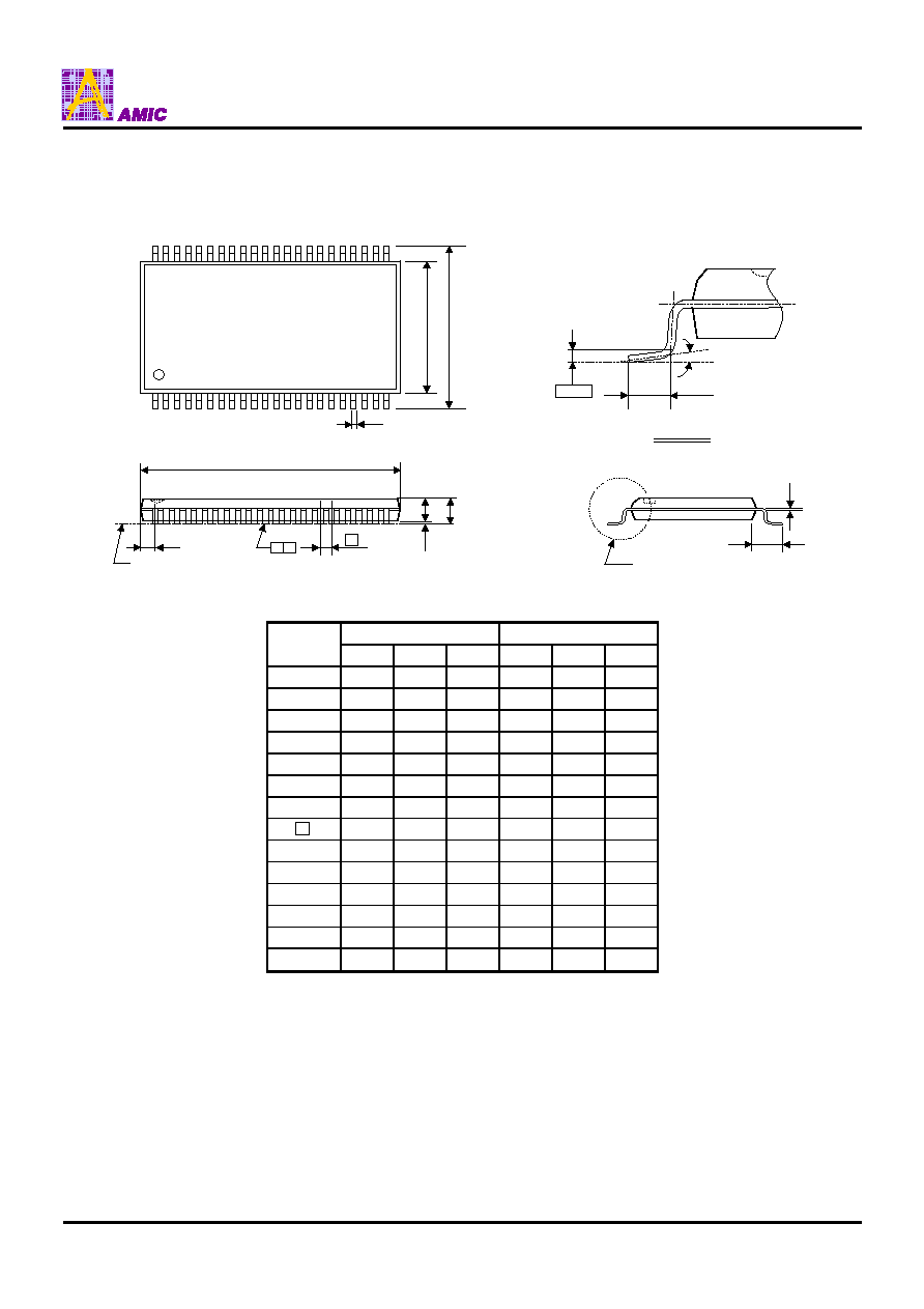
A29L160A Series
(May, 2005, Version 0.1)
39
AMIC Technology, Corp.
Package Information
SOP 44L Outline Dimensions
unit: inches/mm
1
L
L
1
C
22
See Detail F
Detail F
23
44
S
D
Seating Plane
D y
E
H
E
A
1
A
2
A
e
b
0.010"
Gauge Plane
Dimensions in inches
Dimensions in mm
Symbol
Min Nom
Max Min Nom
Max
A - -
0.118
- -
3.00
A
1
0.004
- -
0.10
- -
A
2
0.103
0.106
0.109
2.62
2.69
2.77
b 0.013
0.016
0.020
0.33
0.40
0.50
C 0.007
0.008
0.010
0.18
0.20
0.25
D
- 1.122
1.130
- 28.50
28.70
E 0.490
0.496
0.500
12.45
12.60
12.70
e
- 0.050
- - 1.27 -
H
E
0.620
0.631
0.643
15.75
16.03
16.33
L 0.024
0.032
0.040
0.61
0.80
1.02
L
1
- 0.0675
- - 1.71 -
S - -
0.045
- -
1.14
y - -
0.004
- -
0.10
0
�
-
8
�
0
�
-
8
�
Notes:
1. The maximum value of dimension D includes end flash.
2. Dimension E does not include resin fins.
3. Dimension S includes end flash.

A29L160A Series
(May, 2005, Version 0.1)
40
AMIC Technology, Corp.
Package Information
TSOP 48L (Type I) Outline Dimensions
unit: inches/mm
1
E
c
D
L
Detail "A"
0.25
24
25
48
D
1
D
y
e
S
A
1
A
2
A
Detail "A"
b
Dimensions in inches
Dimensions in mm
Symbol
Min Nom
Max Min Nom
Max
A -
-
0.047
-
-
1.20
A
1
0.002
- 0.006
0.05 - 0.15
A
2
0.037
0.039
0.042
0.94
1.00
1.06
b 0.007
0.009
0.011
0.18
0.22
0.27
c 0.004
-
0.008
0.12 - 0.20
D 0.779
0.787
0.795
19.80
20.00
20.20
D
1
0.720
0.724
0.728
18.30
18.40
18.50
E -
0.472
0.476
-
12.00
12.10
e
0.020 BASIC
0.50 BASIC
L 0.016
0.020
0.024
0.40
0.50
0.60
S
0.011 Typ.
0.28 Typ.
y -
-
0.004
-
-
0.10
0� - 8� 0� - 8�
Notes:
1. The maximum value of dimension D includes end flash.
2. Dimension E does not include resin fins.
3. Dimension S includes end flash.

A29L160A Series
(May, 2005, Version 0.1)
41
AMIC Technology, Corp.
Package Information
48 Balls CSP (6 x 8 mm) Outline Dimensions
unit: mm
(48TFBGA)
A
1
H
G
F
E
D
C
B
A
TOP VIEW
SIDE VIEW
C
SEATING PLANE
1 2 3 4 5 6
BOTTOM VIEW
Ball*A1 CORNER
H
G
F
E
D
C
B
A
E
E
1
e
e
D
1
D
b
0.10 C
A
Dimensions in mm
Symbol
Min.
Nom.
Max.
A -
-
1.20
A
1
0.20
0.25
0.30
b 0.30
-
0.40
D 5.90
6.00
6.10
D
1
4.00
BSC
e -
0.80
-
E 7.90
8.00
8.10
E
1
5.60
BSC