Äîêóìåíòàöèÿ è îïèñàíèÿ www.docs.chipfind.ru

A416316B Series
Preliminary
64K X 16 CMOS DYNAMIC RAM WITH FAST PAGE MODE
PRELIMINARY (November, 2000, Version 0.0)
AMIC Technology, Inc.
Document Title
64K X 16 CMOS DYNAMIC RAM WITH FAST PAGE MODE
Revision History
Rev. No. History
Issue Date
Remark
0.0
Initial issue
November 15, 2000
Preliminary
A416316B Series
Preliminary
64K X 16 CMOS DYNAMIC RAM WITH FAST PAGE MODE
PRELIMINARY (November, 2000, Version 0.0) 1
AMIC Technology, Inc.
Features
n
Organization: 65,536 words X 16 bits
n
Part Identification:
-
A416316B
-
A416316B-L (with self-refresh mode)
n
High speed
- 30/35/40 ns RAS access time
- 16/18/20 ns column address access time
- 10/11/12 ns CAS access time
n
Low power consumption
- Operating: 75mA (-30 max)
-
Standby: 3 mA (TTL)
n
Separate CAS (
UCAS
, LCAS ) for byte selection
n
Self refresh mode
n
256 refresh cycles, 4 ms refresh interval
n
Read-modify-write, RAS -only, CAS -before- RAS ,
Hidden refresh capability
n
TTL-compatible, three-state I/O
n
JEDEC standard packages
-
400mil, 40-pin SOJ
-
400mil, 40/44 TSOP type II package
n
Single 5V power supply/built-in VBB generator
Pin Configuration
Pin Descriptions
n
n
SOJ
n
n
TSOP
VCC
I/O
0
I/O
1
NC
A1
A2
A3
VCC
A4
A5
A6
A7
NC
I/O
13
I/O
14
I/O
15
VSS
A416316BS
21
WE
RAS
I/O
12
OE
I/O
2
I/O
3
I/O
4
I/O
5
I/O
6
I/O
7
A0
NC
NC
VCC
VSS
UCAS
LCAS
NC
I/O
8
I/O
9
I/O
10
I/O
11
VSS
20
19
18
12
16
17
13
14
15
11
10
9
8
7
6
5
4
3
2
1
22
23
24
25
26
27
28
29
30
31
32
33
34
35
36
37
38
39
40
VCC
I/O
0
I/O
1
NC
A1
A2
A3
A4
A5
A6
A7
NC
I/O
13
I/O
14
I/O
15
VSS
A416316BV
23
WE
RAS
I/O
12
OE
I/O
2
I/O
3
I/O
4
I/O
5
I/O
6
I/O
7
A0
NC
NC
VCC
VSS
UCAS
LCAS
NC
I/O
8
I/O
9
I/O
10
I/O
11
VSS
22
21
20
14
18
19
15
16
17
13
10
9
8
7
6
5
4
3
2
1
24
25
26
27
28
29
30
31
32
35
36
37
38
39
40
41
42
43
44
VCC
Symbol
Description
A0 A7
Address Inputs
I/O
0
- I/O
15
Data Input/Output
RAS
Row Address Strobe
UCAS
Column Address Strobe/Upper Byte Control
LCAS
Column Address Strobe/Lower Byte Control
WE
Write Enable
OE
Output Enable
VCC
+5V Power Supply
VSS
Ground
NC
No Connection
A416316B Series
PRELIMINARY (November, 2000, Version 0.0) 2
AMIC Technology, Inc.
Selection Guide
Symbol
Description
-30
-35
-40
Unit
t
RAC
Maximum RAS Access Time
30
35
40
ns
t
AA
Maximum Column Address Access Time
16
18
20
ns
t
CAC
Maximum CAS Access Time
10
11
12
ns
t
OEA
Maximum Output Enable ( OE ) Access Time
10
11
12
ns
t
RC
Minimum Read or Write Cycle Time
65
70
75
ns
t
PC
Minimum Fast Page Mode Cycle Time
19
21
23
ns
I
CC1
Maximum Operating Current
95
85
75
mA
I
CC6
Maximum CMOS Standby Current
2
2
2
mA
Functional Description
The A416316B is a high performance CMOS Dynamic
Random Access Memory organized as 65,536 words X
16 bits. The A416316B is fabricated with advanced
CMOS technology and designed with innovative design
techniques resulting in high speed, extremely low power
and wide operating margins at component and system
levels.
The A416316B features a high speed page mode
operation in which high speed read, write and read-write
are performed on any of the bits defined by the column
address. The asynchronous column address uses an
extremely short row address capture time to ease the
system level timing constraints associated with
multiplexed addressing. Output is tri-stated by a column
address strobe ( UCAS and LCAS ) which acts as an
output enable independent of RAS . Very fast UCAS and
LCAS to output access time eases system design.
All inputs are TTL compatible. Fast Page Mode
operation allows random access up to 256 X 16 bits
within a page, with cycle time as short as 19/21/23 ns.
The A416316B is best suited for graphics, digital signal
processing and high performance peripherals.
The A416316B is available in JEDEC standard 40-pin
plastic SOJ package and 40/44 TSOP type II package.
A416316B Series
PRELIMINARY (November, 2000, Version 0.0) 3
AMIC Technology, Inc.
Block Diagram
RAS CLOCK
GENERATOR
UPPER
BYTE
DATA
I/O
BUFFER
SENSE AMP
COLUMN
DECODER
REFRESH
CONTROLLER
ADDRESS BUFFERS
WE CLOCK
GENERATOR
UCAS CLOCK
GENERATOR
SUBSTRATE
BIAS
GENERATOR
256 X 256 X 16
ARRAY
ROW DECODER
RAS
UCAS
A0
A7
A6
A5
A4
A3
A2
A1
VSS
VCC
I/O
8
I/O
9
I/O
10
I/O
11
Y0 - Y7
256
X0 - X7
I/O
12
I/O
13
I/O
14
I/O
15
OE CLOCK
GENERATOR
WE
OE
LCAS CLOCK
GENERATOR
LCAS
256 X 16
LOWER
BYTE
DATA
I/O
BUFFER
I/O
0
I/O
1
I/O
2
I/O
3
I/O
4
I/O
5
I/O
6
I/O
7
Recommended Operating Conditions
(Ta = 0
°
C to +70
°
C)
Symbol
Description
Min.
Typ.
Max.
Unit
VCC
Supply Voltage
4.5
5.0
5.5
V
VSS
0.0
0.0
0.0
V
V
IH
Input Voltage
2.4
-
VCC + 1
V
V
IL
-1.0
-
0.8
V
A416316B Series
PRELIMINARY (November, 2000, Version 0.0) 4
AMIC Technology, Inc.
Truth Table
Function
RAS
UCAS
LCAS
WE
OE
Address
I/Os
Notes
Standby
H
H
H
L
L
L
L
Read: Word
L
L
L
H
L
Row/Col.
Data Out
Read: Lower Byte
L
H
L
H
L
Row/Col.
I/O
0-7
= Data Out
I/O
8-15
= High-Z
Read: Upper Byte
L
L
H
H
L
Row/Col.
I/O
0-7
= High-Z
I/O
8-15
= Data Out
Write: Word(Early)
L
L
L
L
X
Row/Col.
Data In
Write: Lower Byte(Early)
L
H
L
L
X
Row/Col.
I/O
0-7
= Data In
I/O
8-15
= X
Write: Upper Byte(Early)
L
L
H
L
X
Row/Col.
I/O
0-7
= X
I/O
8-15
= Data In
Read-Write
L
L
L
H
L
L
H
Row/Col. Data Out
Data In
1.2
Fast-Page-Mode Read: Hi-Z
-First cycle
-Subsequent Cycles
L
L
H
L
H
L
H
L
H
L
H
H
H
L
H
L
Row/Col.
Col.
Data Out
Data Out
2
2
Fast-Page-Mode Write(Early)
-First cycle
-Subsequent Cycles
L
L
H
L
H
L
H
L
H
L
L
L
X
X
Row/Col.
Col.
Data In
Data In
1
1
Fast-Page-Mode Read-Write
-First cycle
-Subsequent Cycles
L
L
H
L
H
L
H
L
H
L
H
L
H
L
L
H
L
H
Row/Col.
Col.
Data In
Data In
1, 2
1, 2
Hidden Refresh Read
L
H
L
L
L
H
L
Row/Col.
Data Out
2
Hidden Refresh Write
L
H
L
L
L
L
X
Row/Col.
Data In
High-Z
1
RAS
-Only Refresh
L
H
H
X
X
Row
High-Z
CBR Refresh
H
L
L
L
X
X
X
High-Z
3
Self Refresh (L-ver only)
H
L
L
L
X
X
X
High-Z
Note: 1. Byte Write may be executed with either
UCAS
or
LCAS
active.
2. Byte Read may be executed with either
UCAS
or
LCAS
active.
3. Only one
CAS
signal (
UCAS
or
LCAS
) must be active.
A416316B Series
PRELIMINARY (November, 2000, Version 0.0) 5
AMIC Technology, Inc.
Absolute Maximum Ratings*
Input Voltage (Vin) . . . . . . . . . . . . . . . . . . . -1.0V to +7.0V
Output Voltage (Vout) . . . . . . . . . . . . . . . . -1.0V to +7.0V
Power Supply Voltage (VCC) . . . . . . . . . . -1.0V to +7.0V
Operating Temperature (T
OPR
) . . . . . . . . . . 0
°
C to +70
°
C
Storage Temperature (T
STG
) . . . . . . . . . -55
°
C to +150
°
C
Soldering Temperature X Time (T
SLODER
) . . . . . . . . . . . . . .
. . . . . . . . . . . . . . . . . . . . . . . . . . . . . . . . . 260
°
C X 10sec
Power Dissipation (P
D
) . . . . . . . . . . . . . . . . . . . . . . . . 1W
Short Circuit Output Current (Iout) . . . . . . . . . . . . . 50mA
Latch-up Current . . . . . . . . . . . . . . . . . . . . . . . . . . 200mA
*Comments
Stresses above those listed under "Absolute Maximum
Ratings" may cause permanent damage to this device.
These are stress ratings only. Functional operation of
this device at these or any other conditions above
those indicated in the operational sections of these
specification is not implied or intended. Exposure to
the absolute maximum rating conditions for extended
periods may affect device reliability.
DC Electrical Characteristics
(VCC = 5V
±
10%, VSS = 0V, Ta = 0
°
C to +70
°
C)
Symbol
Parameter
-30
-35
-40
Unit
Test Conditions
Notes
Min.
Max.
Min.
Max.
Min.
Max.
I
IL
Input Leakage Current
-10
+10
-10
+10
-10
+10
µ
A
0V
Vin
+5.5V
Pins not under test = 0V
I
OL
Output Leakage
Current
-10
+10
-10
+10
-10
+10
µ
A
DOUT disabled,
0V
Vout
+5.5V
I
CC1
Operating Current
-
95
-
85
-
75
mA
RAS
,
UCAS
,
LCAS
Address cycling
t
RC
= min.
1, 2
I
CC2
TTL Standby Power
Supply Current
-
3
-
3
-
3
mA
RAS
=
CAS
V
IH
All other inputs
VSS
I
CC3
Refresh Current
(
RAS
only Refresh)
-
95
-
85
-
75
mA
RAS
cycling,
UCAS
=
LCAS
= V
IH
,
t
RC
= min.
1
I
CC4
Fast Page Mode
Current
-
95
-
85
-
75
mA
RAS
= V
IL
,
UCAS
,
LCAS
Address cycling
t
PC
= min.
1, 2
I
CC5
Refresh Current
(
CAS
-before-
RAS
Refresh )
-
95
-
85
-
75
mA
RAS
,
UCAS
,
LCAS
cycling
t
RC
= min.
1
I
CC6
CMOS Standby
Power Supply Current
-
2
-
2
-
2
mA
RAS
=
CAS
VCC - 0.2V
All other inputs
VSS
I
CC7
Self Refresh Mode
Current
-
3
-
3
-
3
mA
RAS
=
CAS
VSS + 0.2V
All other inputs
VSS
V
OH
Output High Voltage
2.4
-
2.4
-
2.4
-
V
I
OUT
= -5.0mA
V
OL
Output Low Voltage
-
0.4
-
0.4
-
0.4
V
I
OUT
= 4.2mA
A416316B Series
PRELIMINARY (November, 2000, Version 0.0) 6
AMIC Technology, Inc.
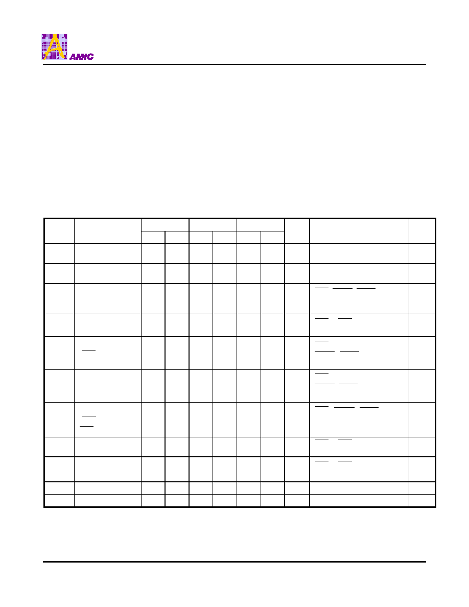
AC Characteristics
(VCC = 5V
±
10%, VSS = 0V, Ta = 0
°
C to +70
°
C)
#
Std
Symbol
Parameter
-30
-35
-40
Unit
Notes
Min. Max. Min. Max. Min. Max.
1
t
RC
Random Read or Write Cycle Time
65
-
70
-
75
-
ns
2
t
RP
RAS
Precharge Time
25
-
25
-
25
-
ns
3
t
RAS
RAS
Pulse Width
30
75K
35
75K
40
75K
ns
4
t
CAS
CAS
Pulse Width
12
-
12
-
12
-
ns
5
t
RCD
RAS
to CAS Delay Time
15
20
16
24
17
28
ns
6
6
t
RAD
RAS
to Column Address Delay Time
10
14
11
17
12
20
ns
7
7
t
RSH
CAS
to RAS Hold Time
10
-
10
-
10
-
ns
8
t
CSH
CAS
Hold Time
30
-
35
-
40
-
ns
9
t
CRP
CAS
to RAS Precharge Time
5
-
5
-
5
-
ns
10
t
ASR
Row Address Setup Time
0
-
0
-
0
-
ns
11
t
RAH
Row Address Hold Time
5
-
6
-
7
-
ns
t
T
Transition Time (Rise and Fall)
2
50
2
50
2
52
ns
4, 5
t
REF
Refresh Period
-
4
-
4
-
4
ms
3
12
t
CLZ
CAS
to Output in Low Z
0
-
0
-
0
-
ns
8
13
t
RAC
Access Time from RAS
-
30
-
35
-
40
ns
6,7
14
t
CAC
Access Time from CAS
-
10
-
11
-
12
ns
6, 13
15
t
AA
Access Time from Column Address
-
16
-
18
-
20
ns
7, 13
16
t
AR
Column Address Hold Time from RAS
26
-
28
-
30
-
ns
17
t
RCS
Read Command Setup Time
0
-
0
-
0
-
ns
A416316B Series
PRELIMINARY (November, 2000, Version 0.0) 7
AMIC Technology, Inc.
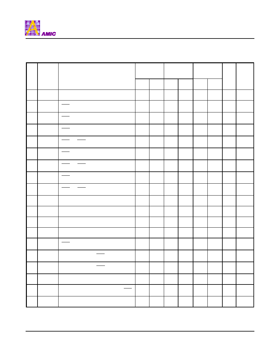
AC Characteristics (continued)
(VCC = 5V
±
10%, VSS = 0V, Ta = 0
°
C to +70
°
C)
#
Std
Symbol
Parameter
-30
-35
-40
Unit
Notes
Min. Max. Min. Max. Min. Max.
18
t
RCH
Read Command Hold Time
0
-
0
-
0
-
ns
9
19
t
RRH
Read Command Hold Time Reference
to RAS
0
-
0
-
0
-
ns
9
20
t
RAL
Column Address to RAS Lead Time
16
-
18
-
20
-
ns
21
t
COH
Output Hold After CAS Low
5
-
5
-
5
-
ns
22
t
ODS
Output Disable Setup Time
0
-
0
-
0
-
ns
23
t
OFF
Output Buffer Turn-Off Delay Time
0
6
0
6
0
6
ns
8, 10
24
t
ASC
Column Address Setup Time
0
-
0
-
0
-
ns
25
t
CAH
Column Address Hold Time
5
-
5
-
5
-
ns
26
t
RPS
RAS
Precharge Setup Time
50
-
60
-
70
-
ns
27
t
WCS
Write Command Setup Time
0
-
0
-
0
-
ns
11
28
t
WCH
Write Command Hold Time
5
-
5
-
5
-
ns
11
29
t
WCR
Write Command Hold Time to RAS
26
-
28
-
30
-
ns
30
t
WP
Write Command Pulse Width
5
-
5
-
5
-
ns
31
t
RWL
Write Command to RAS Lead Time
10
-
11
-
12
-
ns
32
t
CWL
Write Command to CAS Lead Time
10
-
11
-
12
-
ns
33
t
DS
Data-in setup Time
0
-
0
-
0
-
ns
12
34
t
DH
Data-in Hold Time
5
-
5
-
5
-
ns
12
35
t
DHR
Data-in Hold Time to RAS
26
-
28
-
30
-
ns
36
t
RMW
Read-Modify-Write Cycle Time
100
-
105
-
100
-
ns
37
t
RWD
RAS
to WE Delay Time
(Read-Modify-Write)
50
-
54
-
58
-
ns
11
A416316B Series
PRELIMINARY (November, 2000, Version 0.0) 8
AMIC Technology, Inc.
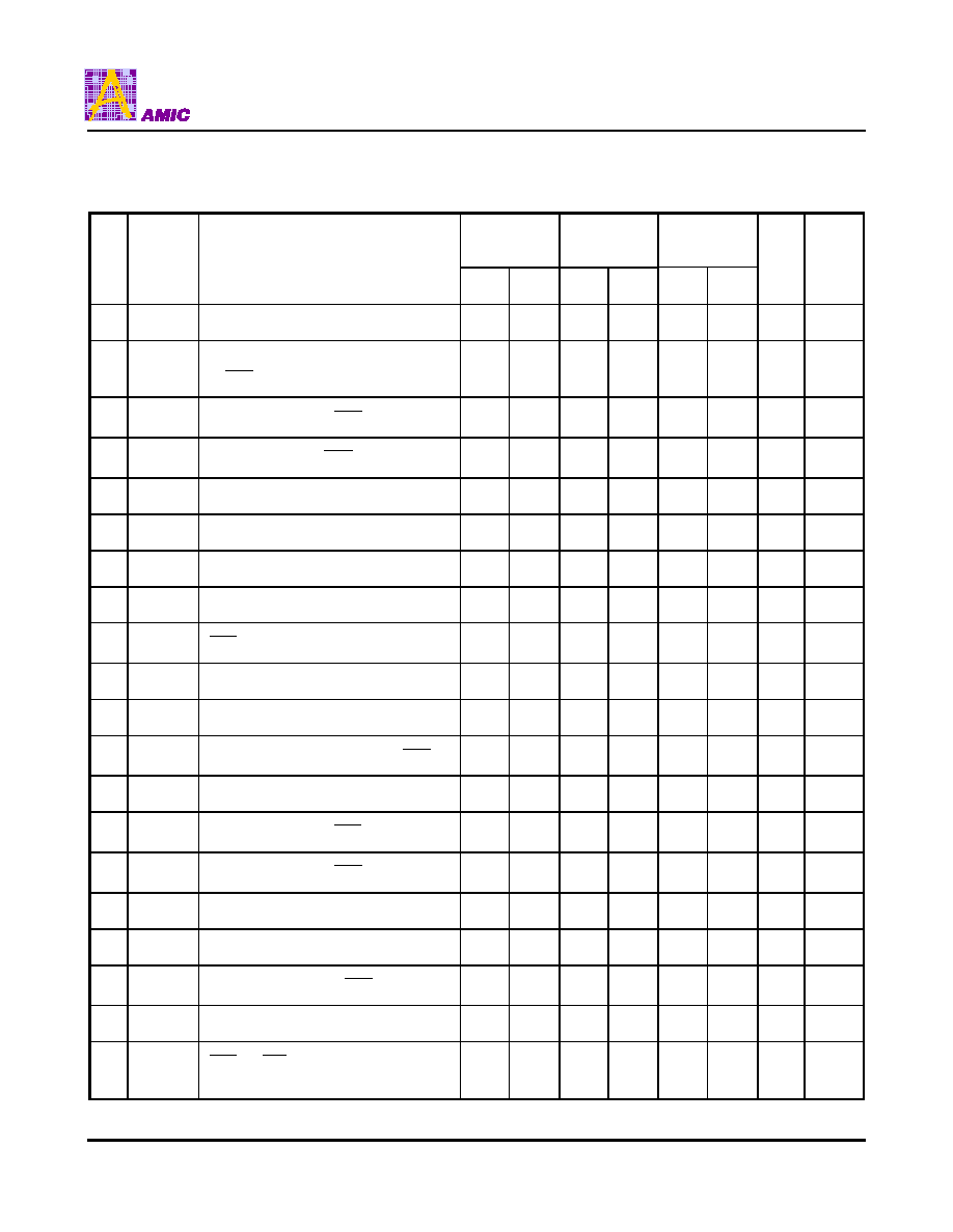
AC Characteristics (continued)
(VCC = 5V
±
10%, VSS = 0V, Ta = 0
°
C to +70
°
C)
#
Std
Symbol
Parameter
-30
-35
-40
Unit
Notes
Min. Max. Min. Max. Min. Max.
38
t
CWD
CAS
to WE Delay Time
(Read-Modify-Write)
26
-
28
-
30
-
ns
11
39
t
AWD
Column Address to WE Delay Time
(Read-Modify-Write)
32
-
35
-
35
-
ns
11
40
t
RASS
RAS
Pulse Width (Self Refresh Mode)
300
-
300
-
300
-
µ
s
41
t
CPN
CAS
Precharge Time
( CAS before RAS )
10
100K
10
100K
10
100K
ns
42
t
PC
Read or Write Cycle Time (Fast Page)
19
-
21
-
23
-
ns
14
43
t
CPA
Access Time from CAS Precharge
(Fast Page)
-
19
-
21
-
23
ns
13
44
t
CP
CAS
Precharge Time (Fast Page)
3
-
4
-
5
-
ns
45
t
PRM
Fast Page Mode RMW Cycle Time
56
-
58
-
60
-
ns
46
t
CRW
Fast Page Mode CAS Pulse Width
(RMW)
-
44
-
46
-
48
ns
47
t
RASP
RAS
Pulse Width (Fast Page)
30
75K
35
75K
40
75K
ns
48
t
CSR
CAS
Setup Time ( CAS -before- RAS )
0
-
0
-
0
-
ns
3
49
t
CHR
CAS
Hold Time ( CAS -before- RAS )
7
-
8
-
8
-
ns
3
50
t
RPC
RAS
to CAS Precharge Time
( CAS -before- RAS )
0
-
0
-
0
-
ns
51
t
ROH
RAS
Hold Time Reference to OE
6
-
7
-
8
-
ns
52
t
OEA
OE
Access Time
-
10
-
11
-
12
ns
53
t
OED
OE
to Data Delay
5
-
5
-
5
-
ns
54
t
OEZ
Output Buffer Turn-off Delay from OE
0
5
0
6
0
6
ns
8
A416316B Series
PRELIMINARY (November, 2000, Version 0.0) 9
AMIC Technology, Inc.
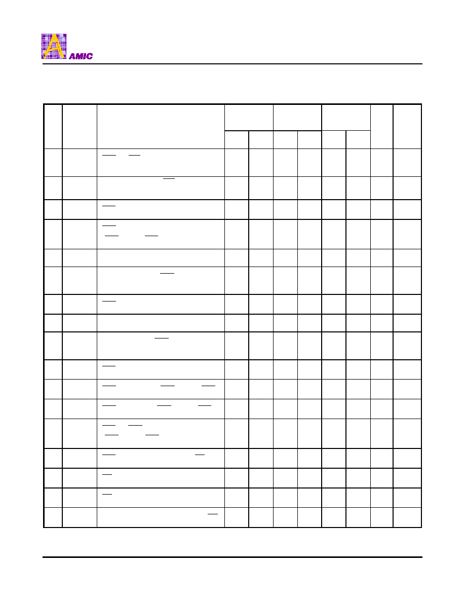
AC Characteristics (continued)
(VCC = 5V
±
10%, VSS = 0V, Ta = 0
°
C to +70
°
C)
#
Std
Symbol
Parameter
-30
-35
-40
Unit
Notes
Min. Max. Min. Max. Min. Max.
55
t
OEH
OE
Command Hold Time
0
-
0
-
0
-
ns
56
t
CPT
CAS
Precharge Time
( CAS -before- RAS Counter Test)
20
-
20
-
20
-
ns
Notes:
1. I
CC1
, I
CC3
, I
CC4
, and I
CC5
depend on cycle rate.
2. I
CC1
and I
CC4
depend on output loading. Specified values are obtained with the outputs open.
3. An initial pause of 200
µ
s is required after power-up followed by any 8 RAS cycles before proper device operation is
achieved. In the case of an internal refresh counter, a minimum of 8 CAS -before- RAS initialization cycles instead of 8
RAS cycles are required. 8 initialization cycles are required after extended periods of bias without clocks (greater than
8ms).
4. AC Characteristics assume t
T
= 3ns. All AC parameters are measured with a load equivalent to one TTL loads and
50pF, V
IL
(min.)
GND and V
IH
(max.)
VCC.
5. V
IH
(min.) and V
IL
(max.) are reference levels for measuring timing of input signals. Transition times are measured
between V
IH
and V
IL
.
6. Operation within the t
RCD
(max.) limit insures that t
RAC
(max.) can be met. t
RCD
(max.) is specified as a reference
point only. If t
RCD
is greater than the specified t
RCD
(max.) limit, then access time is controlled exclusively by t
CAC
.
7. Operation within the t
RAD
(max.) limit insures that t
RAC
(max.) can be met. t
RAD
(max.) is specified as a reference
point only. If t
RAD
is greater than the specified t
RAD
(max.) limit, then access time is controlled exclusively by t
AA
.
8. Assumes three state test load (5pF and a 380
Thevenin equivalent).
9. Either t
RCH
or t
RRH
must be satisfied for a read cycle.
10. t
OFF
(max.) defines the time at which the output achieves the open circuit condition; it is not referenced to output
voltage levels.
11. t
WCS
, t
WCH
, t
RWD
, t
CWD
and t
AWD
are not restrictive operating parameters. They are included in the data sheet
as electrical characteristics only. If t
WCS
t
WCS
(min.) and t
WCH
t
WCH
(min.), the cycle is an early write cycle
and data-out pins will remain open circuit, high impedance, throughout the entire cycle. If t
RWD
t
RWD
(min.) , t
CWD
t
CWD
(min.) and t
AWD
t
AWD
(min.), the cycle is a read-modify-write cycle and the data out will contain data read from
the selected cell. If neither of the above conditions is satisfied, the condition of the data out at access time is
indeterminate.
12. These parameters are referenced to
UCAS
and
LCAS
leading edge in early write cycles and to WE leading edge in
read-modify-write cycles.
13. Access time is determined by the longer of t
AA
or t
CAC
or t
CPA
.
14. t
ASC
t
CP
to achieve t
PC
(min.) and t
CPA
(max.) values.
15. These parameters are sampled and not 100% tested.
A416316B Series
PRELIMINARY (November, 2000, Version 0.0) 10
AMIC Technology, Inc.
t
RAS(3)
t
RP(2)
t
RC(1)
t
CRP(9)
t
CSH(8)
t
RCD(5)
t
RSH(7)
t
CAS(4)
t
ASR(10)
t
CRP(9)
t
RAH(11)
t
ASC(24)
t
CAH(25)
t
RAD(6)
t
RAL(20)
t
RCH(18)
t
RRH(19)
t
AR(16)
t
RCS(17)
t
ROH(51)
t
OEA(52)
t
RAC(13)
t
AA(15)
t
CAC(14)
t
CLZ(12)
t
OEZ(54)
t
OFF(23)
High-Z
: High or Low
Valid Data-out
Row Address
Column Address
I/O
0
~
I/O
15
OE
WE
A0 ~ A7
UCAS
LCAS
RAS
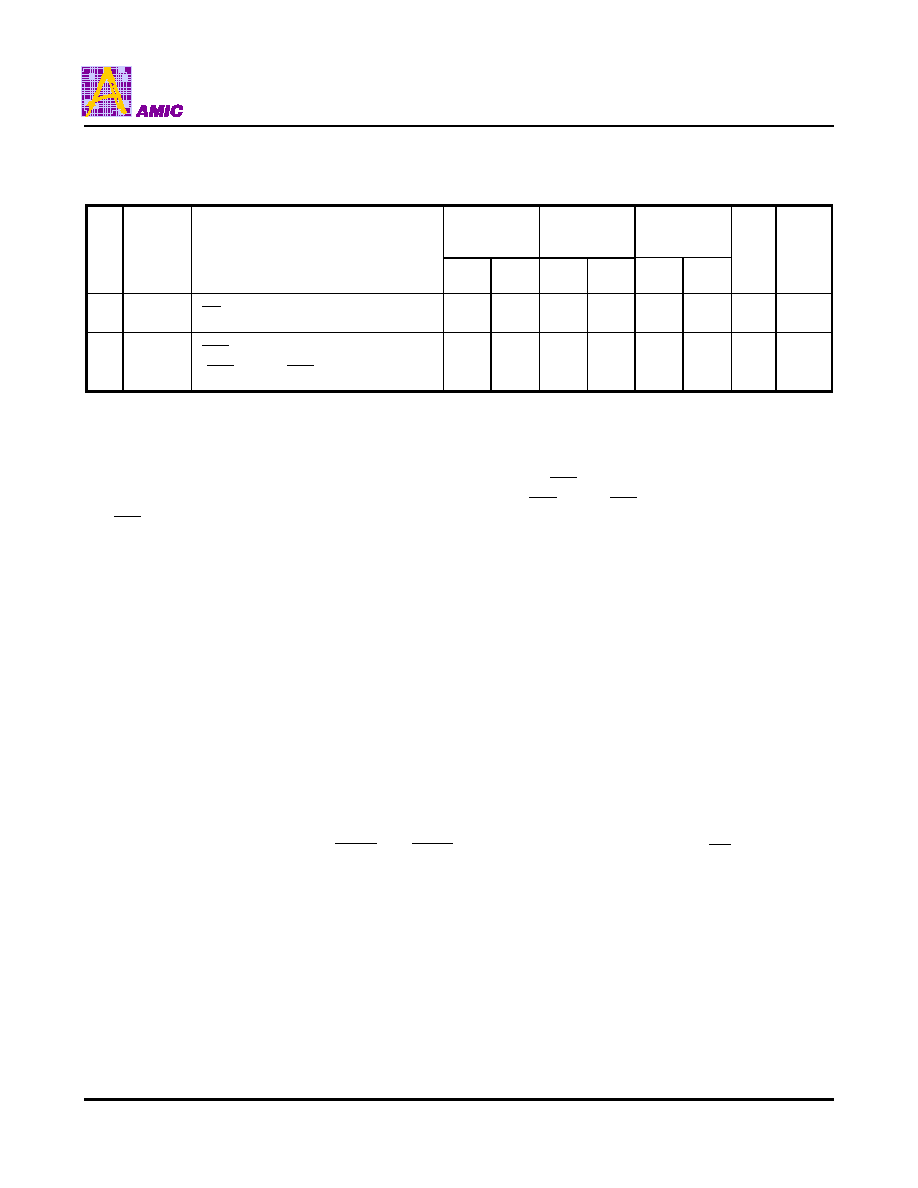
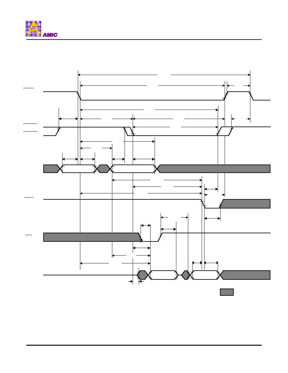
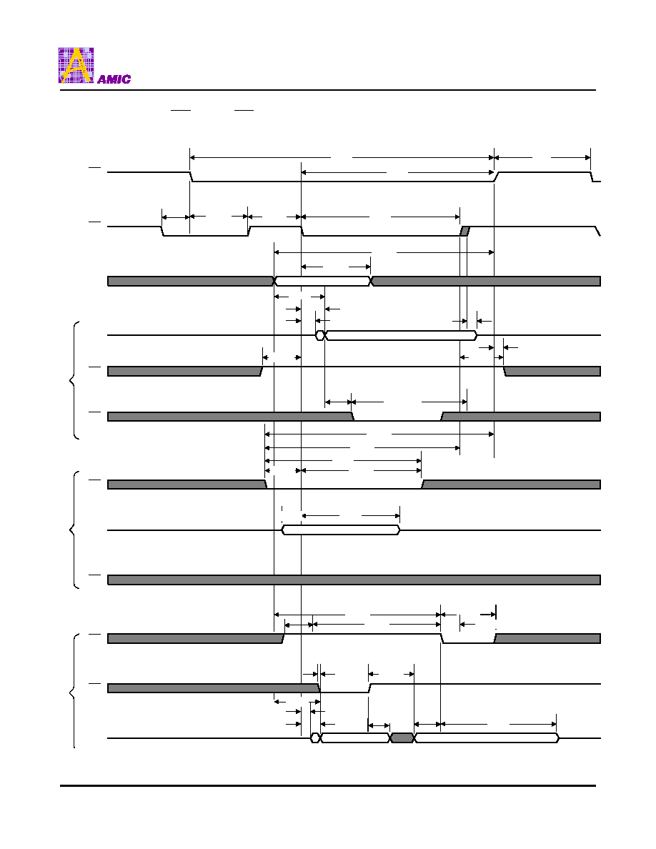
Word Read Cycle
A416316B Series
PRELIMINARY (November, 2000, Version 0.0) 11
AMIC Technology, Inc.
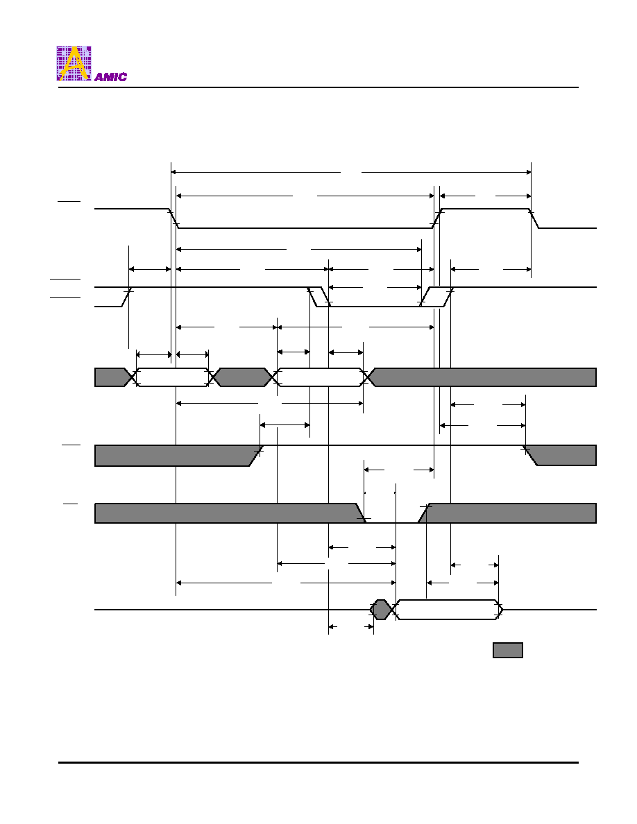
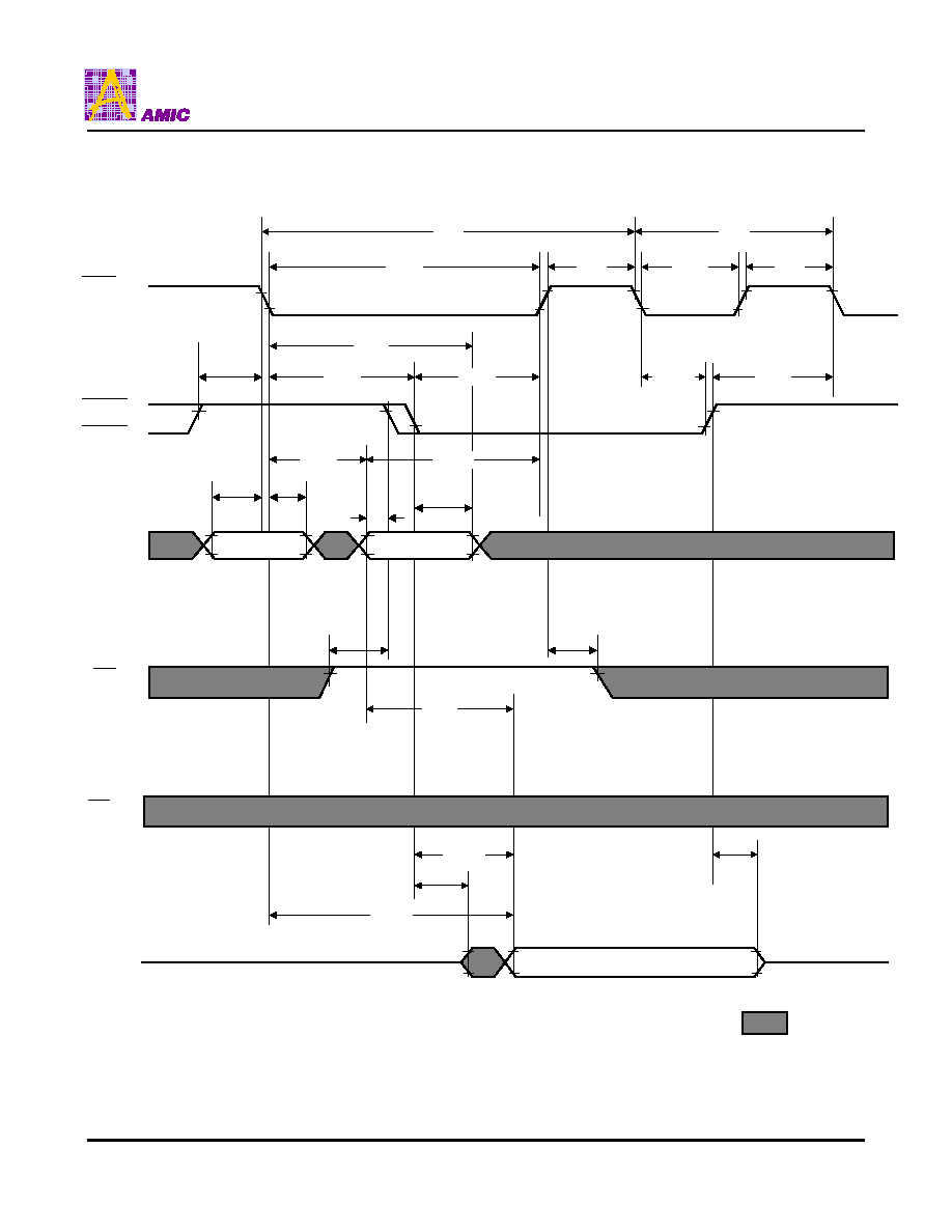
Word Write Cycle (Early Write)
t
RAS(3)
t
RP(2)
t
RC(1)
t
CRP(9)
t
CSH(8)
t
RCD(5)
t
RSH(7)
t
CAS(4)
t
ASR(10)
t
CRP(9)
t
RAH(11)
t
ASC(24)
t
CAH(25)
t
RAD(6)
t
RAL(20)
t
WCH(28)
: High or Low
Row Address
Column Address
I/O
0
~
I/O
15
OE
A0 ~ A7
UCAS
LCAS
RAS
t
AR(16)
t
CWL(32)
t
RWL(31)
t
WP(30)
t
WCS(27)
Valid Data-in
t
DS(33)
t
DH(34)
WE
t
WCR(29)
t
DHR(35)
A416316B Series
PRELIMINARY (November, 2000, Version 0.0) 12
AMIC Technology, Inc.
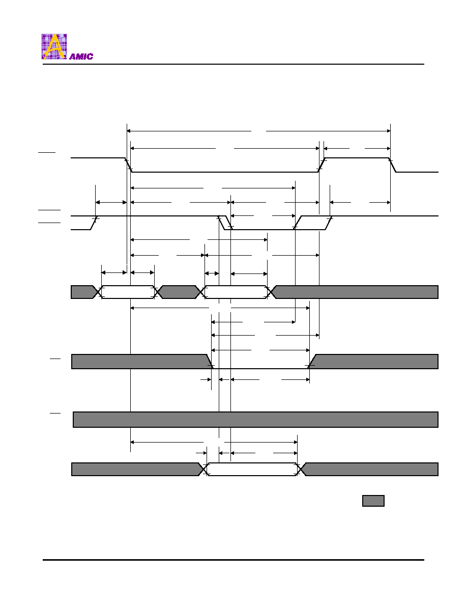
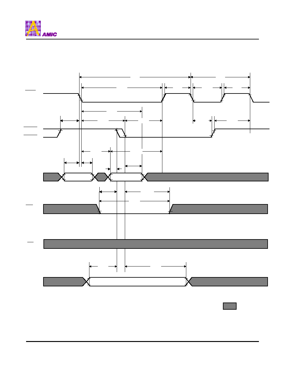
Word Write Cycle (
Late Write)
t
RAS(3)
t
RP(2)
t
RC(1)
t
CRP(9)
t
CSH(8)
t
RCD(5)
t
RSH(7)
t
CAS(4)
t
ASR(10)
t
CRP(9)
t
ASC(24)
t
CAH(25)
t
RAD(6)
t
RAL(20)
Row Address
Column Address
A0 ~ A7
UCAS
LCAS
RAS
t
AR(16)
t
CWL(32)
t
RWL(31)
t
WP(30)
t
RAH(11)
t
OEH(55)
t
OED(54)
t
DS(33)
t
DH(34)
I/O
0
~
I/O
15
: High or Low
OE
WE
High-Z
Vaild Data-in
t
WCR(29)
t
DHR(35)
A416316B Series
PRELIMINARY (November, 2000, Version 0.0) 13
AMIC Technology, Inc.
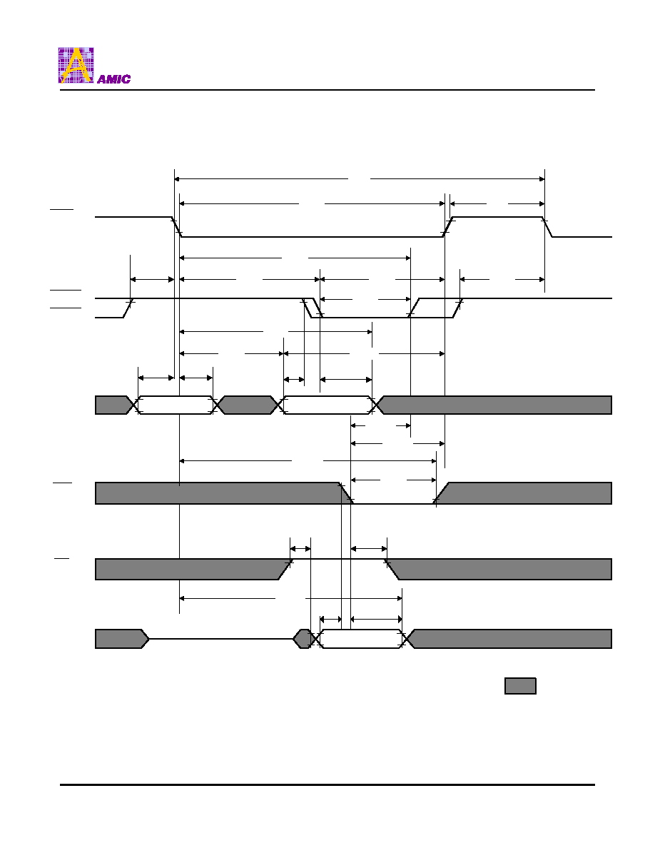
Word Read-Modify-Write Cycle
t
RAS(3)
t
RP(2)
t
RMW(36)
t
CRP(9)
t
CSH(8)
t
RCD(5)
t
RSH(7)
t
CAS(4)
t
ASR(10)
t
CRP(9)
t
RAH(11)
t
CAH(25)
t
RAD(6)
Row Address
Column Address
A0 ~ A7
UCAS
LCAS
RAS
t
AR(16)
t
RWL(31)
t
ASC(24)
t
CWL(32)
t
AWD(39)
t
CWD38)
t
RWD(37)
t
WP(30))
t
OEA(52)
t
OEZ(54)
t
CLZ(12)
t
CAC(14)
t
OED(53)
t
AA(15)
t
RAC(13)
t
DS(33)
t
DH(34)
High-Z
Data-out
Data-in
: High or Low
I/O
0
~
I/O
15
OE
WE

A416316B Series
PRELIMINARY (November, 2000, Version 0.0) 14
AMIC Technology, Inc.
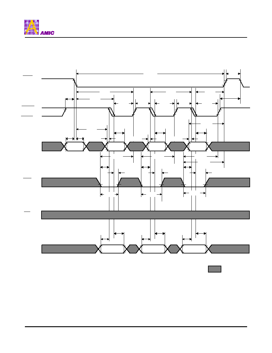
Fast Page Mode Word Read Cycle
t
RASP(47)
t
RP(2)
RAS
UCAS
LCAS
t
CAS(4)
t
CP(44)
t
CAS(4)
t
CP(44)
t
CAS(4)
t
RCD(5)
t
CSH(8)
t
CRP(9)
t
CRP(9)
t
PC(42)
t
RSH(7)
t
ASR(10)
t
RAH(11)
t
RAD(6)
t
AR(16)
t
ASC(24)
t
CAH(25)
t
ASC(24)
t
CAH(25)
t
CAH(25)
t
ASC(24)
t
RAL(20)
t
RCS(17)
t
RCH(18)
t
RCS(17)
t
RCS(17)
t
RCH(18)
t
RRH(19)
t
RCH(18)
t
AA(15)
t
AA(15)
t
OFF(23)
t
OFF(23)
t
CLZ(12)
t
CLZ(12)
t
RAC(13)
t
CAC(14)
t
AA(15)
t
CAC(14)
t
OEA(52)
t
OFF(23)
t
CLZ(12)
t
CAC(14)
t
OEZ(54)
t
OEZ(54)
t
OEZ(54)
t
OEA(52)
t
OEA(52)
t
CPA(43)
t
CPA(43)
t
ROH(51)
Row
Column
Column
A0 ~ A7
OE
WE
I/O
0
~
I/O
15
Data-out
Data-out
Data-out
: High or Low
Column
A416316B Series
PRELIMINARY (November, 2000, Version 0.0) 15
AMIC Technology, Inc.
Fast Page Mode Early Word Write Cycle
t
RASP(47)
t
RP(2)
RAS
UCAS
LCAS
t
CAS(4)
t
CP(44)
t
CAS(4)
t
CP(44)
t
CAS(4)
t
RCD(5)
t
CSH(8)
t
CRP(9)
t
CRP(9)
t
PC(42)
t
RSH(7)
t
ASR(10)
t
RAH(11)
t
RAD(6)
t
ASC(24)
t
CAH(25)
t
ASC(24)
t
CAH(25)
t
CAH(25)
t
ASC(24)
t
RAL(20)
Row
Column
Column
A0 ~ A7
WE
t
CWL(32)
t
WCH(28)
t
WCS(27)
t
WCS(27)
Column
t
CWL(32)
t
WCH(28)
t
WCS(27)
t
WCH(28)
t
CWL(32)
t
RWL(31)
t
WP(30)
t
WP(30)
t
WP(30)
t
DH(34)
t
DS(33)
t
DH(34)
t
DS(33)
t
DS(33)
t
DH(34)
Data-in
Data-in
Data-in
I/O
0
~
I/O
15
OE
: High or Low
A416316B Series
PRELIMINARY (November, 2000, Version 0.0) 16
AMIC Technology, Inc.
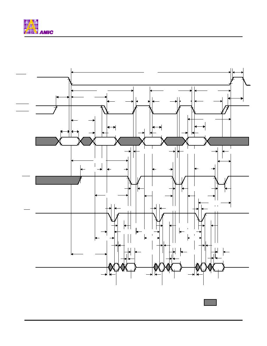
Fast Page Mode Word Read-Modify-Write Cycle
t
RASP(47)
RAS
t
CAS(4)
t
CP(44)
t
CAS(4)
t
CP(44)
t
CAS(4)
t
RCD(5)
t
CSH(8)
t
CRP(9)
t
CRP(9)
t
PRMW(45)
t
RSH(7)
t
RP(2)
t
ASR(10)
t
RAH(11)
t
RAD(6)
t
ASC(24)
t
CAH(25)
t
ASC(24)
t
CAH(25)
t
ASC(24)
t
CAH(25)
t
RAL(20)
t
RCS(17)
t
CWD(38)
t
RWD(37)
t
CWL(32)
t
CWD(38)
t
CWL(32)
t
CWD(38)
t
CWL(32)
t
RWL(31)
t
OEA(52)
t
OEA(52)
t
OEA(52)
t
WP(30)
t
WP(30)
t
WP(30)
t
AWD(39)
t
AWD(39)
t
AWD(39)
t
ROH(51)
t
CAC(14)
t
AA(15)
t
RAC(13)
t
OED(53)
t
OEZ(54)
t
DS(33)
t
AA(15)
t
CPA(43)
t
DH(34)
t
OEZ(54)
t
OED(53)
t
DS(33)
t
DH(34)
t
OEZ(54)
t
DS(33)
t
OED(53)
t
DH(34)
t
AA(15)
t
CPA(43)
t
CLZ(12)
t
CLZ(12)
t
CLZ(12)
High-Z
: High or Low
I/O
0
~
I/O
15
OE
WE
A0 ~ A7
UCAS
LCAS
Data-out
Data-in
Data-out
Data-in
Data-out
Data-in
Row
Column
Column
Column
A416316B Series
PRELIMINARY (November, 2000, Version 0.0) 17
AMIC Technology, Inc.
RAS
Only Refresh Cycle
CAS
Before RAS
Refresh Cycle
t
RAS(3)
t
RP(2)
t
RC(1)
RAS
t
CRP(9)
t
RPC(50)
t
ASR(10)
t
RAH(11)
A0 ~ A7
UCAS
LCAS
: High or Low
Row
Note: WE, OE = Don't care.
t
RAS(3)
t
RP(2)
t
RC(1)
RAS
t
RP(2)
t
RPC(50)
t
CPN(41)
t
CSR(48)
t
CHR(49)
t
OFF(23)
I/O
0
~
I/O
15
UCAS
LCAS
High-Z
: High or Low
Note: WE, OE, A0 ~ A7 = Don't care.
A416316B Series
PRELIMINARY (November, 2000, Version 0.0) 18
AMIC Technology, Inc.
Timing Waveform of
CAS
-before-
RAS
Refresh Counter Test Cycle
t
CAC
(14)
t
RAS
(3)
t
RSH
(7)
t
RP
(2)
t
CPT
(56)
t
CHR
(49)
t
CAS
(4)
t
RAL
(20)
t
CAH
(25)
t
AA
(15)
t
CAC
(14)
t
CLZ
(12)
t
OFF
(23)
t
RCH
(18)
t
RCS
(17)
t
RRH
(19)
t
RWL
(31)
t
CWL
(32)
t
WP
(30)
t
WCH
(28)
t
WCS
(27)
t
DH
(34)
t
DS
(33)
t
WP
(30)
t
CWL
(32)
t
AWD
(39)
t
CWD
(38)
t
OED
(53)
t
OEA
(52)
t
DH
(34)
t
CLZ
(12)
t
AA
(15)
Col Address
Data Out
Data In
Data In
Data Out
RAS
CAS
Address
WE
I/O
OE
I/O
I/O
WE
OE
WE
OE
Read Cycle
Write Cycle
Read-Write Cycle
t
OEA
(52)
t
ROH
(53)
t
CSR
(48)
t
RCS
(17)
t
DS
(33)
t
OEZ
(54)
A416316B Series
PRELIMINARY (November, 2000, Version 0.0) 19
AMIC Technology, Inc.
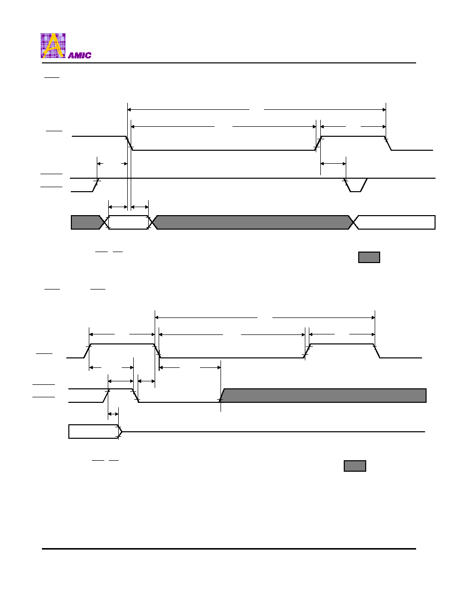
Hidden Refresh Cycle (Word Read)
t
RAS(3)
t
RP(2)
t
RC(1)
t
CRP(9)
t
AR(16)
t
RCD(5)
t
ASR(10)
t
CRP(9)
t
ASC(24)
t
CAH(25)
t
RAD(6)
A0 ~ A7
UCAS
LCAS
RAS
t
RAH(11)
t
RRH(19)
t
RCS(17)
I/O
0
~
I/O
15
: High or Low
OE
High-Z
t
RAS(3)
t
RP(2)
t
CHR(49)
t
RC(1)
t
RSH(7)
t
RAL(20)
t
CAC(14)
t
OFF(23)
t
AA(15)
t
CLZ(12)
t
RAC(13)
WE
Row
Column
Valid Data-out
A416316B Series
PRELIMINARY (November, 2000, Version 0.0) 20
AMIC Technology, Inc.
Hidden Refresh Cycle (Early Word Write)
t
RAS(3)
t
RP(2)
t
RC(1)
t
CRP(9)
t
AR(16)
t
RCD(5)
t
ASR(10)
t
CRP(9)
t
ASC(24)
t
CAH(25)
t
RAD(6)
A0 ~ A7
RAS
t
RAH(11)
: High or Low
OE
t
RAS(3)
t
RP(2)
t
CHR(49)
t
RC(1)
t
RSH(7)
t
RAL(20)
WE
Row
Column
t
WCS(27)
t
WCH(28)
t
WP(30)
t
DS(33)
t
DH(34)
Valid Data-in
I/O
0
~
I/O
15
UCAS
LCAS
A416316B Series
PRELIMINARY (November, 2000, Version 0.0) 21
AMIC Technology, Inc.
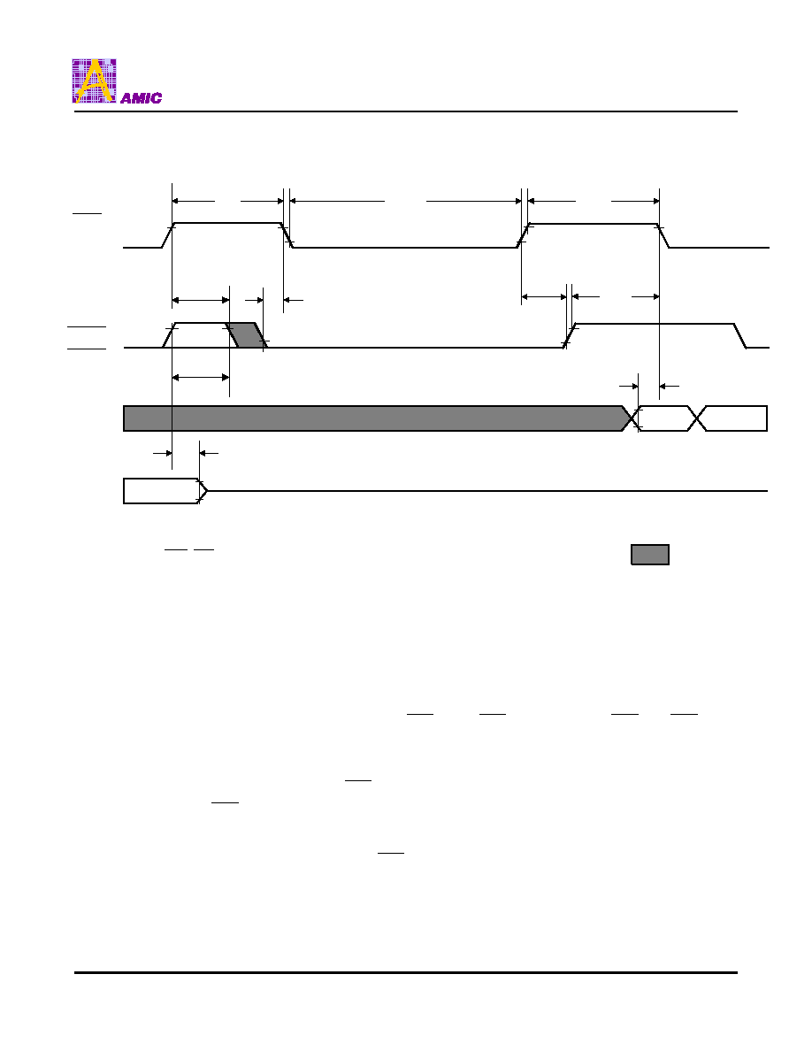
Self Refresh Mode (A416316B-L Only)
n
Self Refresh Mode.
a. Entering the Self Refresh Mode:
The A416316B-L Self Refresh Mode is entered by using
CAS
before
RAS
cycle and holding
RAS
and
CAS
signal
"low" longer than 300
µ
s.
b. Continuing the Self Refresh Mode:
The Self Refresh Mode is continued by holding
RAS
"low" after entering the Self Refresh Mode.
It does not depend on
CAS
being "high" or "low" after entering the Self Refresh Mode continue the Self Refresh Mode.
c. Exiting the Self Refresh Mode:
The A416316B exits the Self Refresh Mode when the
RAS
signal is brought "high".
t
RASS(40)
t
PR(2)
t
CRP(9)
t
CSR(48)
t
RPC(50)
RAS
t
RPS(26)
t
CHS(21)
t
ASR(10)
t
CPN(41)
t
OFF(23)
A0 ~ A7
: High or Low
High-Z
I/O
0
~
I/O
15
UCAS
LCAS
ROW
COL
Note: WE, OE = Don't care.
A416316B Series
PRELIMINARY (November, 2000, Version 0.0) 22
AMIC Technology, Inc.
Capacitance
15
(f = 1MHz, Ta = Room Temperature, VCC = 5V
±
10%)
Symbol
Signals
Parameter
Max.
Unit
Test Conditions
C
IN1
A0 A7
5
pF
Vin = 0V
C
IN2
RAS
,
UCAS
,
LCAS
, WE ,
OE
Input Capacitance
7
pF
Vin = 0V
C
I/O
I/O
0
- I/O
15
I/O Capacitance
7
pF
Vin = Vout = 0V
Ordering Codes
Package\ RAS Access Time
30ns
35ns
40ns
Self-Refresh
40L SOJ (400 mil)
A416316BS-30
A416316BS-35
A416316BS-40
No
40/44L TSOP type II (400mil)
A416316BV-30
A416316BV-35
A416316BV-40
No
40L SOJ (400mil)
A416316BS-30L
A416316BS-35L
A416316BS-40L
Yes
40/44L TSOP II (400mil)
A416316BV-30L
A416316BV-35L
A416316BV-40L
Yes
A416316B Series
PRELIMINARY (November, 2000, Version 0.0) 23
AMIC Technology, Inc.
Package Information
SOJ 40L Outline Dimensions
unit: inches/mm
Dimensions in inches
Dimensions in mm
Symbol
Min
Nom
Max
Min
Nom
Max
A
-
-
0.144
-
-
3.66
A
1
0.025
-
-
0.64
-
-
A
2
0.105
0.110
0.115
2.67
2.79
2.92
b
1
0.026
0.028
0.032
0.66
0.71
0.81
b
0.016
0.018
0.022
0.41
0.46
0.56
C
0.008
0.010
0.014
0.20
0.25
0.36
D
1.020
1.025
1.030
25.91
26.04
26.16
E
0.395
0.400
0.405
10.03
10.16
10.29
e
0.044
0.050
0.056
1.12
1.27
1.42
e
1
0.355
0.366
0.376
9.114
9.383
9.652
H
E
0.430
0.440
0.450
10.92
11.18
11.43
L
0.081
0.093
0.105
2.083
2.39
2.70
S
-
-
0.050
-
-
1.27
y
-
-
0.004
-
-
0.10
0
°
-
10
°
0
°
-
10
°
Notes:
1. The maximum value of dimension D includes end flash.
2. Dimension E does not include resin fins.
3. Dimension e
1
is for PC Board surface mount pad pitch design
reference only.
4. Dimension S includes end flash.
1
E
H
E
20
21
40
A
1
A
2
e
e
1
C
S
D
Seating Plane
D
y
L
1
A
b
b
A416316B Series
PRELIMINARY (November, 2000, Version 0.0) 24
AMIC Technology, Inc.
Package Information
TSOP 40/44L (Type II) Outline Dimensions
unit: inches/mm
1
E
H
E
L
1
L
1
c
44
A
1
A
2
A
S
D
y
e
D
B
L
L
Dimensions in inches
Dimensions in mm
Symbol
Min
Nom
Max
Min
Nom
Max
A
-
-
0.047
-
-
1.20
A
1
0.002
-
0.006
0.05
-
0.15
A
2
0.037
0.039
0.041
0.95
1.00
1.05
B
0.013
0.015
0.017
0.32
0.37
0.42
c
0.003
0.005
0.009
0.08
0.13
0.23
D
0.720
0.725
0.730
18.28
18.41
18.54
E
0.395
0.400
0.405
10.03
10.16
10.29
e
0.031 BSC
0.80 BSC
H
E
0.455
0.463
0.471
11.56
11.76
11.96
L
0.016
0.020
0.024
0.40
0.50
0.60
L
1
-
0.031
-
-
0.80
-
S
-
-
0.035
-
-
0.90
y
-
-
0.004
-
-
0.10
1°
3°
5°
1°
3°
5°
Notes:
1. The maximum value of dimension D includes end flash.
2. Dimension E does not include resin fins.
3. Dimension S includes end flash.