A420616 Series
Preliminary
1M X 16 CMOS DYNAMIC RAM WITH EDO PAGE MODE
PRELIMINARY (June, 2002, Version 0.2)
1
AMIC Technology, Inc.
Features
n
Organization: 1,048,576 words X 16 bits
n
Part Identification
- A420616 (1K Ref.)
n
Single 5.0V power supply/built-in VBB generator
n
Low power consumption
- Operating: 120mA (-45 max)
-
Standby: 1.0mA (TTL), 1.0mA (CMOS)
1.5mA (Self-refresh current)
n
High speed
- 45/50 ns RAS access time
- 20/22 ns column address access time
-
12/13 ns CAS access time
-
18/20 ns EDO Page Mode Cycle Time
n
Industrial operating temperature range: -40
°
C to 85
°
C
for -U
n
Fast Page Mode with Extended Data Out
n
Separate CAS (
UCAS
,
LCAS
) for byte selection
n
1K Refresh Cycle in 16ms
n
Read-modify-write, RAS -only, CAS -before- RAS ,
Hidden refresh capability
n
TTL-compatible, three-state I/O
n
JEDEC standard packages
-
400mil, 42-pin SOJ
-
400mil, 44/50 TSOP type II package
General Description
The A420616 is a new generation randomly accessed
memory for graphics, organized in a 1,048,576-word by
16-bit configuration. This product can execute Byte Write
and Byte Read operation via two CAS pins.
The A420616 offers an accelerated Fast Page Mode
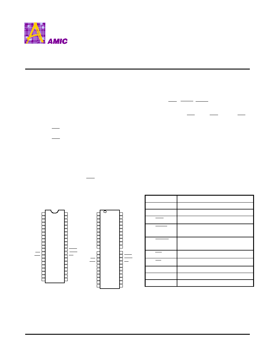
Pin Configuration
n
n
SOJ
n
n
TSOP
VCC
I/O
0
I/O
1
NC
NC
A1
A2
A3
A4
A5
A6
A7
A8
I/O
13
I/O
14
I/O
15
VSS
A420616S
23
WE
RAS
I/O
12
OE
I/O
2
I/O
3
I/O
4
I/O
5
I/O
6
I/O
7
NC
NC
VCC
UCAS
LCAS
NC
I/O
8
I/O
9
I/O
10
I/O
11
VSS
20
19
18
12
16
17
13
14
15
11
10
9
8
7
6
5
4
3
2
1
24
25
26
27
28
29
30
31
32
33
34
35
36
37
38
39
40
41
42
VCC
I/O
0
I/O
1
NC
A0
A1
A2
A4
A5
A6
A7
A8
I/O
13
I/O
14
I/O
15
VSS
A420616V
24
WE
RAS
I/O
12
I/O
2
I/O
3
I/O
4
I/O
5
I/O
6
I/O
7
NC
NC
NC
VCC
VSS
LCAS
UCAS
NC
I/O
8
I/O
9
I/O
10
I/O
11
VSS
21
20
19
13
17
18
14
15
16
12
10
9
8
7
6
5
4
3
2
1
25
26
27
28
29
30
31
32
33
35
36
37
38
39
40
41
42
43
44
VCC
OE
21
22
VSS
VCC
A0
A9
11
22
23
A3
A9
NC
34
NC
cycle with a feature called Extended Data Out (EDO).
This allow random access of up to 1024 words within a
row at a 56/50 MHz EDO cycle, making the A420616
ideally suited for graphics, digital signal processing and
high performance computing systems.
Pin Descriptions
Symbol
Description
A0 A9
Address Inputs
I/O
0
- I/O
15
Data Input/Output
RAS
Row Address Strobe
LCAS
Column Address Strobe for Lower Byte
(I/O
0
I/O
7
)
UCAS
Column Address Strobe for Upper Byte
(I/O
8
I/O
15
)
WE
Write Enable
OE
Output Enable
VCC
5.0V Power Supply
VSS
Ground
NC
No Connection
A420616 Series
PRELIMINARY
(June, 2002, Version 0.2)
2
AMIC Technology, Inc.
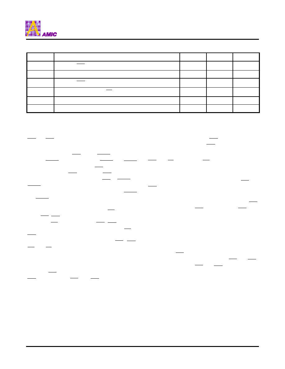
Selection Guide
Symbol
Description
-45
-50
Unit
t
RAC
Maximum RAS Access Time
45
50
ns
t
AA
Maximum Column Address Access Time
20
22
ns
t
CAC
Maximum CAS Access Time
12
13
ns
t
OEA
Maximum Output Enable ( OE ) Access Time
12
13
ns
t
RC
Minimum Read or Write Cycle Time
76
84
ns
t
PC
Minimum EDO Cycle Time
18
20
ns
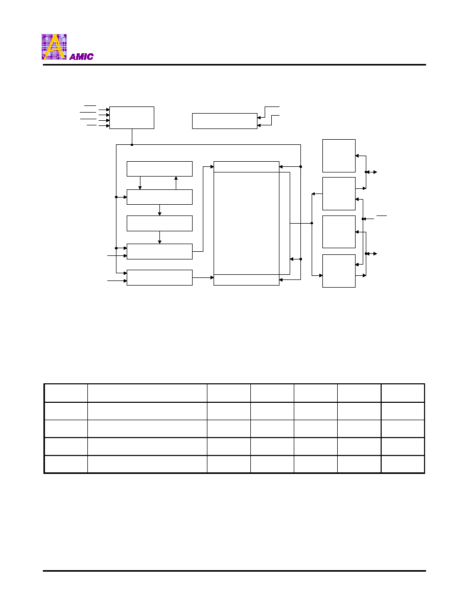
Functional Description
The A420616 reads and writes data by multiplexing an 20-
bit address into a 10-bit row and 10-bit column address.
RAS and CAS are used to strobe the row address and the
column address, respectively.
The A420616 has two CAS inputs:
LCAS
controls I/O
0
-
I/O
7
, and
UCAS
controls I/O
8
-
I/O
15
,
UCAS
and
LCAS
function in an identical manner to CAS in that either will
generate an internal CAS signal. The CAS function and
timing are determined by the first CAS (
UCAS
or
LCAS
) to transition low and by the last to transition high.
Byte Read and Byte Write are controlled by using
LCAS
and
UCAS
separately.
A Read cycle is performed by holding the WE signal high
during RAS / CAS operation. A Write cycle is executed by
holding the WE signal low during RAS / CAS operation;
the input data is latched by the falling edge of WE or
CAS , whichever occurs later. The data inputs and outputs
are routed through 16 common I/O pins, with RAS , CAS ,
WE and OE controlling the in direction.
EDO Page Mode operation all 1024(1K) columns within a
selected row to be randomly accessed at a high data rate.
A EDO Page Mode cycle is initiated with a row address
latched by RAS followed by a column address latched by
CAS . While holding RAS low, CAS can be toggled to
strobe changing column addresses, thus achieving shorter
cycle times.
The A420616 offers an accelerated Fast Page Mode cycle
through a feature called Extended Data Out, which keeps
the output drivers on during the CAS precharge time (t
cp
).
Since data can be output after CAS goes high, the user is
not required to wait for valid data to appear before starting
the next access cycle. Data-out will remain valid as long as
RAS and OE are low, and WE is high; this is the only
characteristic which differentiates Extended Data Out
operation from a standard Read or Fast Page Read.
A memory cycle is terminated by returning both RAS and
CAS high. Memory cell data will retain its correct state by
maintaining power and accessing all 1024(1K)
combinations of the 10-bit row addresses, regardless of
sequence, at least once every 16ms through any RAS
cycle (Read, Write) or RAS Refresh cycle ( RAS -only,
CBR, or Hidden). The CBR Refresh cycle automatically
controls the row addresses by invoking the refresh counter
and controller.
Power-On
The initial application of the VCC supply requires a 200 µs
wait followed by a minimum of any eight initialization cycles
containing a RAS clock. During Power-On, the VCC
current is dependent on the input levels of RAS and CAS .
It is recommended that RAS and CAS track with VCC or
be held at a valid V
IH
during Power-On to avoid current
surges.
A420616 Series
PRELIMINARY
(June, 2002, Version 0.2)
4
AMIC Technology, Inc.
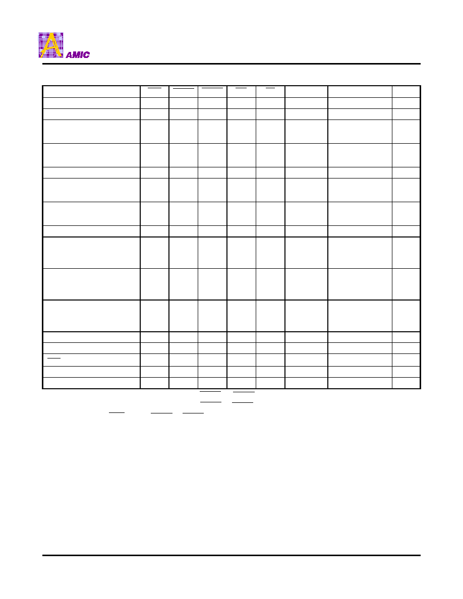
Truth Table
Function
RAS
UCAS
LCAS
WE
OE
Address
I/Os
Notes
Standby
H
H
H
X
X
X
High-Z
Read: Word
L
L
L
H
L
Row/Col.
Data Out
Read: Lower Byte
L
H
L
H
L
Row/Col.
I/O
0-7
= Data Out
I/O
8-15
= High-Z
Read: Upper Byte
L
L
H
H
L
Row/Col.
I/O
0-7
= High-Z
I/O
8-15
= Data Out
Write: Word
L
L
L
L
H
Row/Col.
Data In
Write: Lower Byte
L
H
L
L
H
Row/Col.
I/O
0-7
= Data In
I/O
8-15
= X
Write: Upper Byte
L
L
H
L
H
Row/Col.
I/O
0-7
= X
I/O
8-15
= Data In
Read-Write
L
L
L
H
L
L
H
Row/Col.
Data Out
Data In
1,2
EDO-Page-Mode Read: Hi-Z
-First cycle
-Subsequent Cycles
L
L
H
L
H
L
H
L
H
L
H
H
H
L
H
L
Row/Col.
Col.
Data Out
Data Out
2
2
EDO-Page-Mode Write
-First cycle
-Subsequent Cycles
L
L
H
L
H
L
H
L
H
L
L
L
H
H
Row/Col.
Col.
Data In
Data In
1
1
EDO-Page-Mode Read-Write
-First cycle
-Subsequent Cycles
L
L
H
L
H
L
H
L
H
L
H
L
H
L
L
H
L
H
Row/Col.
Col.
Data Out
Data In
Data Out
Data In
1, 2
1, 2
Hidden Refresh Read
L
H
L
L
L
H
L
Row/Col.
Data Out
2
Hidden Refresh Write
L
H
L
L
L
L
X
Row/Col.
Data In
High-Z
1
RAS -Only Refresh
L
H
H
X
X
Row
High-Z
CBR Refresh
H
L
L
L
X
X
X
High-Z
3
Self Refresh
H
L
L
L
H
X
X
High-Z
Note: 1. Byte Write may be executed with either
UCAS
or
LCAS
active.
2. Byte Read may be executed with either
UCAS
or
LCAS
active.
3. Only one
CAS
signal (
UCAS
or
LCAS
) must be active.