
A426316B Series
Preliminary
64K X 16 CMOS DYNAMIC RAM WITH EDO PAGE MODE
PRELIMINARY (November, 2000, Version 0.0)
AMIC Technology, Inc.
Document Title
64K X 16 CMOS DYNAMIC RAM WITH EDO PAGE MODE
Revision History
Rev. No. History
Issue Date
Remark
0.0
Initial issue
November 15, 2000
Preliminary
A426316B Series
Preliminary
64K X 16 CMOS DYNAMIC RAM WITH EDO PAGE MODE
PRELIMINARY (November, 2000, Version 0.0) 1
AMIC Technology, Inc.
Features
n
Organization: 65,536 words X 16 bits
n
Part Identification:
-
A426316B
-
A426316B-L (with self-refresh mode)
n
High speed
- 30/35/40 ns RAS access time
- 16/18/20 ns column address access time
- 10/11/12 ns CAS access time
n
Low power consumption
- Operating: 75mA (-30 max)
-
Standby: 3 mA (TTL)
n
Separate CAS (
UCAS
, LCAS ) for byte selection
n
Self refresh mode
n
256 refresh cycles, 4 ms refresh interval
n
Read-modify-write, RAS -only, CAS -before- RAS ,
Hidden refresh capability
n
TTL-compatible, three-state I/O
n
JEDEC standard packages
-
400mil, 40-pin SOJ
-
400mil, 40/44 TSOP type II package
n
Single 5V power supply/built-in VBB generator
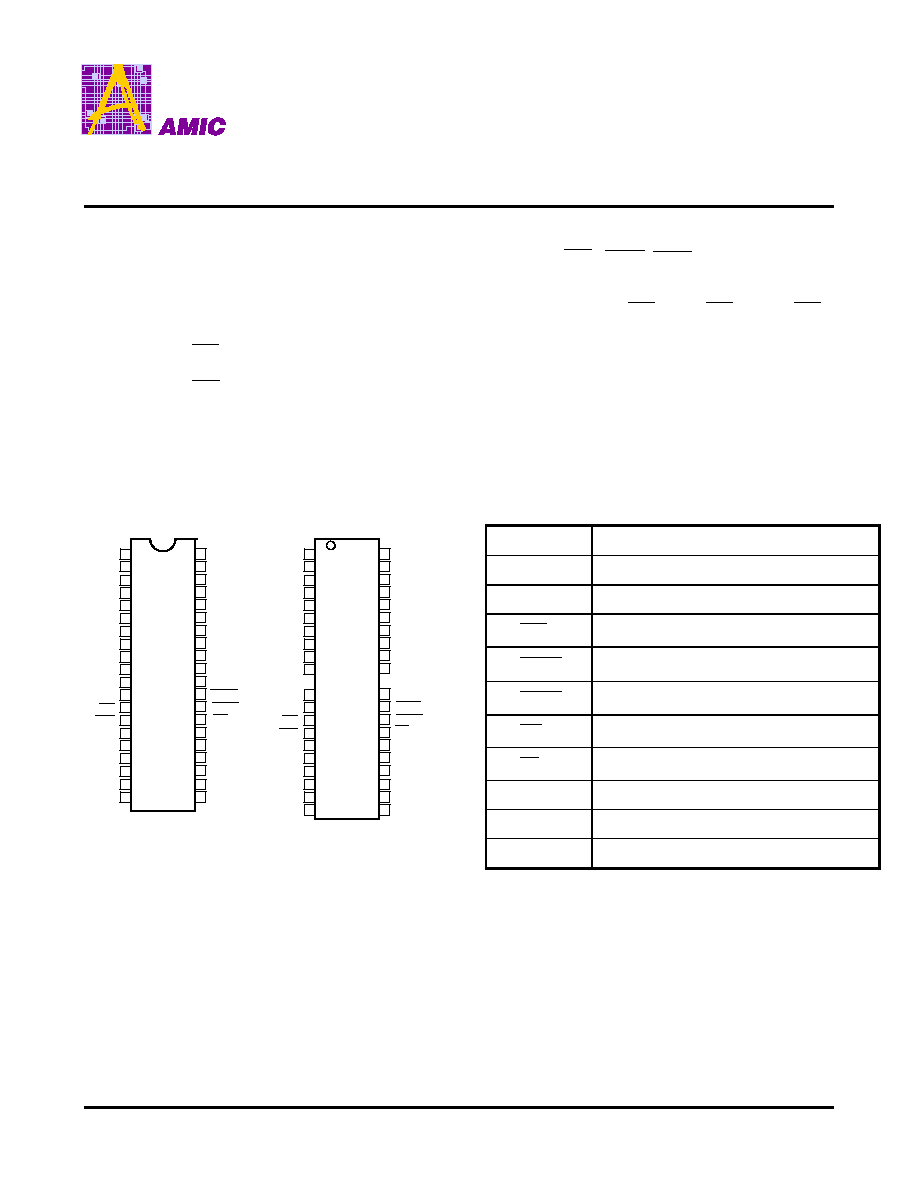
Pin Configuration
Pin Descriptions
n
n
SOJ
n
n
TSOP
VCC
I/O
0
I/O
1
NC
A1
A2
A3
VCC
A4
A5
A6
A7
NC
I/O
13
I/O
14
I/O
15
VSS
A426316BS
21
WE
RAS
I/O
12
OE
I/O
2
I/O
3
I/O
4
I/O
5
I/O
6
I/O
7
A0
NC
NC
VCC
VSS
UCAS
LCAS
NC
I/O
8
I/O
9
I/O
10
I/O
11
VSS
20
19
18
12
16
17
13
14
15
11
10
9
8
7
6
5
4
3
2
1
22
23
24
25
26
27
28
29
30
31
32
33
34
35
36
37
38
39
40
VCC
I/O
0
I/O
1
NC
A1
A2
A3
A4
A5
A6
A7
NC
I/O
13
I/O
14
I/O
15
VSS
A426316BV
23
WE
RAS
I/O
12
OE
I/O
2
I/O
3
I/O
4
I/O
5
I/O
6
I/O
7
A0
NC
NC
VCC
VSS
UCAS
LCAS
NC
I/O
8
I/O
9
I/O
10
I/O
11
VSS
22
21
20
14
18
19
15
16
17
13
10
9
8
7
6
5
4
3
2
1
24
25
26
27
28
29
30
31
32
35
36
37
38
39
40
41
42
43
44
VCC
Symbol
Description
A0 � A7
Address Inputs
I/O
0
- I/O
15
Data Input/Output
RAS
Row Address Strobe
UCAS
Column Address Strobe/Upper Byte Control
LCAS
Column Address Strobe/Lower Byte Control
WE
Write Enable
OE
Output Enable
VCC
+5V Power Supply
VSS
Ground
NC
No Connection
A426316B Series
PRELIMINARY (November, 2000, Version 0.0) 2
AMIC Technology, Inc.
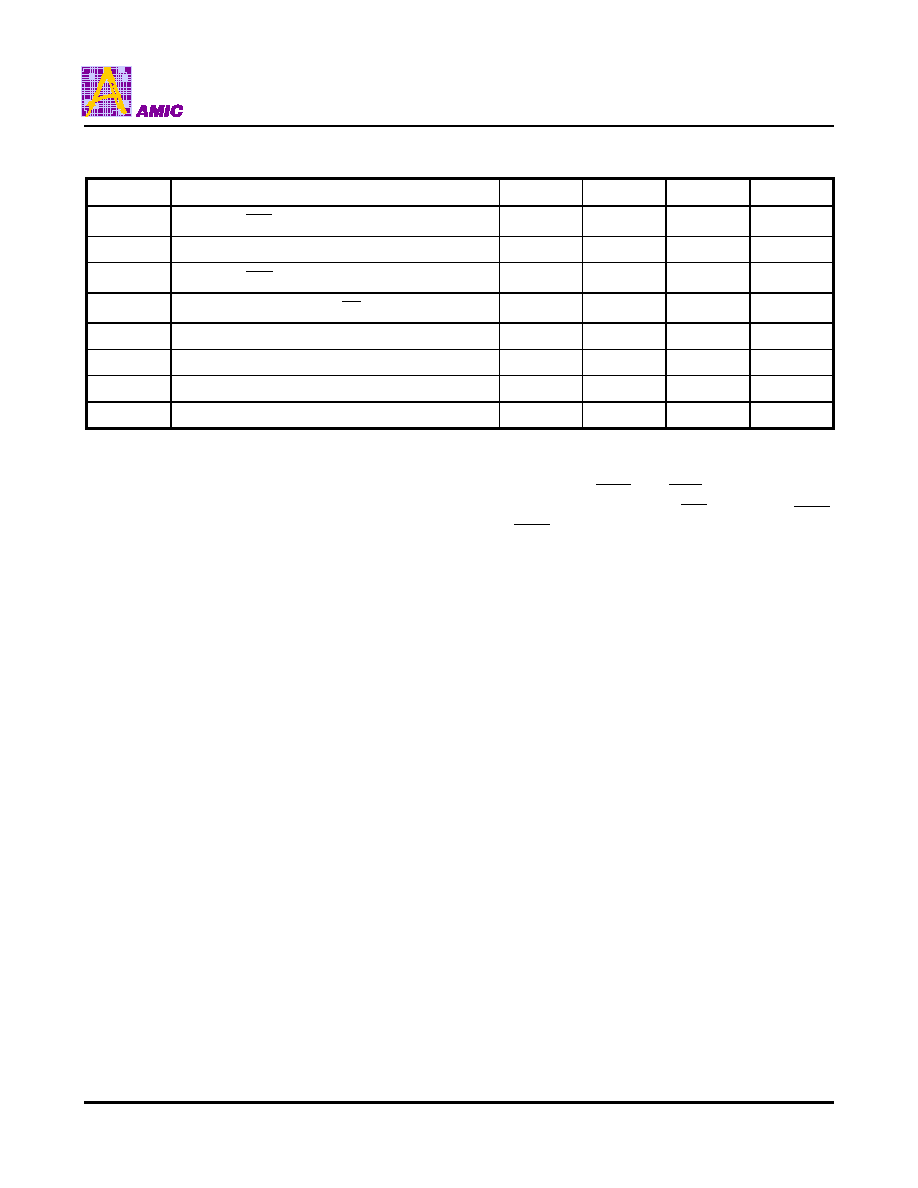
Selection Guide
Symbol
Description
-30
-35
-40
Unit
t
RAC
Maximum RAS Access Time
30
35
40
ns
t
AA
Maximum Column Address Access Time
16
18
20
ns
t
CAC
Maximum CAS Access Time
10
11
12
ns
t
OEA
Maximum Output Enable ( OE ) Access Time
10
11
12
ns
t
RC
Minimum Read or Write Cycle Time
65
70
75
ns
t
PC
Minimum EDO Page Mode Cycle Time
12
14
15
ns
I
CC1
Maximum Operating Current
95
85
75
mA
I
CC6
Maximum CMOS Standby Current
2
2
2
mA
Functional Description
The A426316B is a high performance CMOS Dynamic
Random Access Memory organized as 65,536 words X
16 bits. The A426316B is fabricated with advanced
CMOS technology and designed with innovative design
techniques resulting in high speed, extremely low power
and wide operating margins at component and system
levels.
The A426316B features a high speed page mode
operation in which high speed read, write and read-write
are performed on any of the bits defined by the column
address. The asynchronous column address uses an
extremely short row address capture time to ease the
system level timing constraints associated with
multiplexed addressing. Output is tri-stated by a column
address strobe ( UCAS and LCAS ) which acts as an
output enable independent of RAS . Very EDO UCAS
and LCAS to output access time eases system design.
All inputs are TTL compatible. EDO Page Mode
operation allows random access up to 256 X 16 bits
within a page, with cycle time as short as 12/14/15 ns.
The A426316B is best suited for graphics, digital signal
processing and high performance peripherals.
The A426316B is available in JEDEC standard 40-pin
plastic SOJ package and 40/44 TSOP type II package.
A426316B Series
PRELIMINARY (November, 2000, Version 0.0) 3
AMIC Technology, Inc.
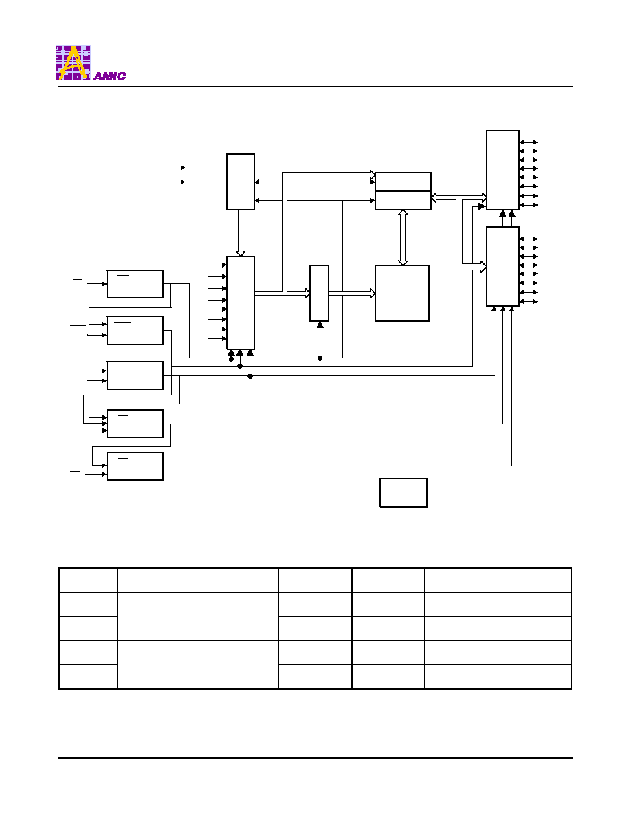
Block Diagram
RAS CLOCK
GENERATOR
UPPER
BYTE
DATA
I/O
BUFFER
SENSE AMP
COLUMN
DECODER
REFRESH
CONTROLLER
ADDRESS BUFFERS
WE CLOCK
GENERATOR
UCAS CLOCK
GENERATOR
SUBSTRATE
BIAS
GENERATOR
256 X 256 X 16
ARRAY
ROW DECODER
RAS
UCAS
A0
A7
A6
A5
A4
A3
A2
A1
VSS
VCC
I/O
8
I/O
9
I/O
10
I/O
11
Y0 - Y7
256
X0 - X7
I/O
12
I/O
13
I/O
14
I/O
15
OE CLOCK
GENERATOR
WE
OE
LCAS CLOCK
GENERATOR
LCAS
256 X 16
LOWER
BYTE
DATA
I/O
BUFFER
I/O
0
I/O
1
I/O
2
I/O
3
I/O
4
I/O
5
I/O
6
I/O
7
Recommended Operating Conditions
(Ta = 0
�
C to +70
�
C)
Symbol
Description
Min.
Typ.
Max.
Unit
VCC
Supply Voltage
4.5
5.0
5.5
V
VSS
0.0
0.0
0.0
V
V
IH
Input Voltage
2.4
-
VCC + 1
V
V
IL
-1.0
-
0.8
V

A426316B Series
PRELIMINARY (November, 2000, Version 0.0) 4
AMIC Technology, Inc.
Truth Table
Function
RAS
UCAS
LCAS
WE
OE
Address
I/Os
Notes
Standby
H
H
H
X
X
X
High-Z
Read: Word
L
L
L
H
L
Row/Col.
Data Out
Read: Lower Byte
L
H
L
H
L
Row/Col.
I/O
0-7
= Data Out
I/O
8-15
= High-Z
Read: Upper Byte
L
L
H
H
L
Row/Col.
I/O
0-7
= High-Z
I/O
8-15
= Data Out
Write: Word(Early)
L
L
L
L
X
Row/Col.
Data In
Write: Lower Byte(Early)
L
H
L
L
X
Row/Col.
I/O
0-7
= Data In
I/O
8-15
= X
Write: Upper Byte(Early)
L
L
H
L
X
Row/Col.
I/O
0-7
= X
I/O
8-15
= Data In
Read-Write
L
L
L
H
L
L
H
Row/Col. Data Out
Data In
1.2
EDO-Page-Mode Read: Hi-Z
-First cycle
-Subsequent Cycles
L
L
H
L
H
L
H
L
H
L
H
H
H
L
H
L
Row/Col.
Col.
Data Out
Data Out
2
2
EDO-Page-Mode Write(Early)
-First cycle
-Subsequent Cycles
L
L
H
L
H
L
H
L
H
L
L
L
X
X
Row/Col.
Col.
Data In
Data In
1
1
EDO-Page-Mode Read-Write
-First cycle
-Subsequent Cycles
L
L
H
L
H
L
H
L
H
L
H
L
H
L
L
H
L
H
Row/Col.
Col.
Data In
Data In
1, 2
1, 2
Hidden Refresh Read
L
H
L
L
L
H
L
Row/Col.
Data Out
2
Hidden Refresh Write
L
H
L
L
L
L
X
Row/Col.
Data In
High-Z
1
RAS
-Only Refresh
L
H
H
X
X
Row
High-Z
CBR Refresh
H
L
L
L
X
X
X
High-Z
3
Self Refresh (L-ver only)
H
L
L
L
X
X
X
High-Z
Note: 1. Byte Write may be executed with either
UCAS
or
LCAS
active.
2. Byte Read may be executed with either
UCAS
or
LCAS
active.
3. Only one
CAS
signal (
UCAS
or
LCAS
) must be active.