
A42U0616 Series
Preliminary
1M X 16 CMOS DYNAMIC RAM WITH EDO PAGE MODE
Preliminary (June, 2001, Version 0.0)
AMIC Technology, Inc.
Document Title
1M X 16 CMOS DYNAMIC RAM WITH EDO PAGE MODE
Revision History
Rev. No. History
Issue Date
Remark
0.0
Initial issue
June 13, 2001
Preliminary

A42U0616 Series
Preliminary
1M X 16 CMOS DYNAMIC RAM WITH EDO PAGE MODE
PRELIMINARY (June, 2001, Version 0.0)
1
AMIC Technology, Inc.
Features
n
Organization: 1,048,576 words X 16 bits
n
Part Identification
- A42U0616 (1K Ref.)
n
Single 2.5V power supply/built-in VBB generator
n
Low power consumption
- Operating: 120mA (-50 max)
-
Standby: 1mA (TTL), 0.2mA (CMOS),
250µA (Self-refresh current)
n
High speed
- 50/60/80 ns RAS access time
- 25/30/40 ns column address access time
-
13/15/20 ns CAS access time
-
20/25/35 ns EDO Page Mode Cycle Time
n
Separate CAS (
UCAS
,
LCAS
) for byte selection
n
Fast Page Mode with Extended Data Out
n
Read-modify-write, RAS -only, CAS -before- RAS ,
Hidden refresh capability
n
TTL-compatible, three-state I/O
n
JEDEC standard packages
-
400mil, 42-pin SOJ
-
400mil, 50/44 TSOP type II package
General Description
The A42U0616 is a new generation randomly accessed
memory for graphics, organized in a 1,048,576 -word by
16-bit configuration. This product can execute Write and
Read operation via CAS pin.
The A42U0616 offers an accelerated Fast Page Mode
cycle with a feature called Extended Data Out (EDO).
Pin Configuration
n
n
SOJ
n
n
TSOP
VCC
I/O
0
I/O
1
NC
NC
A1
A2
A3
A4
A5
A6
A7
A8
I/O
13
I/O
14
I/O
15
VSS
A42U0616S
23
WE
RAS
I/O
12
OE
I/O
2
I/O
3
I/O
4
I/O
5
I/O
6
I/O
7
NC
NC
VCC
UCAS
LCAS
NC
I/O
8
I/O
9
I/O
10
I/O
11
VSS
20
19
18
12
16
17
13
14
15
11
10
9
8
7
6
5
4
3
2
1
24
25
26
27
28
29
30
31
32
33
34
35
36
37
38
39
40
41
42
VCC
I/O
0
I/O
1
NC
A0
A1
A2
A4
A5
A6
A7
A8
I/O
13
I/O
14
I/O
15
VSS
A42U0616V
24
WE
RAS
I/O
12
I/O
2
I/O
3
I/O
4
I/O
5
I/O
6
I/O
7
NC
NC
NC
VCC
VSS
LCAS
UCAS
NC
I/O
8
I/O
9
I/O
10
I/O
11
VSS
21
20
19
13
17
18
14
15
16
12
10
9
8
7
6
5
4
3
2
1
25
26
27
28
29
30
31
32
33
35
36
37
38
39
40
41
42
43
44
VCC
OE
21
22
VSS
VCC
A0
A9
11
22
23
A3
A9
NC
34
NC
This allow random access of up to 1024(1K Ref.) words
within a row at a 50/40/28 MHz EDO cycle, making the
A42U0616 ideally suited for graphics, digital signal
processing and high performance computing systems.
Pin Descriptions
Symbol
Description
A0 - A9
Address Inputs (1K product)
I/O
0
- I/O
15
Data Input/Output
RAS
Row Address Strobe
LCAS
Column Address Strobe for Lower Byte
(I/O
0
≠ I/O
7
)
UCAS
Column Address Strobe for Upper Byte
(I/O
8
≠ I/O
15
)
WE
Write Enable
OE
Output Enable
VCC
2.5V Power Supply
VSS
Ground
NC
No Connection
A42U0616 Series
PRELIMINARY
(June, 2001, Version 0.0)
2
AMIC Technology, Inc.
Selection Guide
Symbol
Description
-50
-60
-80
Unit
t
RAC
Maximum RAS Access Time
50
60
80
ns
t
AA
Maximum Column Address Access Time
25
30
40
ns
t
CAC
Maximum CAS Access Time
13
15
20
ns
t
OEA
Maximum Output Enable ( OE ) Access Time
13
15
20
ns
t
RC
Minimum Read or Write Cycle Time
84
104
134
ns
t
PC
Minimum EDO Cycle Time
20
25
35
ns
Functional Description
The A42U0616 reads and writes data by multiplexing an
20-bit address into a 10-bit row and 10-bit column address.
RAS and CAS are used to strobe the row address and the
column address, respectively.
The A42U0616 has two CAS inputs:
LCAS
controls I/O
0
-
I/O
7
, and
UCAS
controls I/O
8
-
I/O
15
,
UCAS
and
LCAS
function in an identical manner to CAS in that either will
generate an internal CAS signal. The CAS function and
timing are determined by the first CAS (
UCAS
or
LCAS
) to transition low and by the last to transition high.
Byte Read and Byte Write are controlled by using
LCAS
and
UCAS
separately.
A Read cycle is performed by holding the WE signal high
during RAS / CAS operation. A Write cycle is executed by
holding the WE signal low during RAS / CAS operation;
the input data is latched by the falling edge of WE or
CAS , whichever occurs later. The data inputs and outputs
are routed through 16 common I/O pins, with RAS , CAS ,
WE and OE controlling the in direction.
EDO Page Mode operation all 1024(1K) columns within a
selected row to be randomly accessed at a high data rate.
A EDO Page Mode cycle is initiated with a row address
latched by RAS followed by a column address latched by
CAS . While holding RAS low, CAS can be toggled to
strobe changing column addresses, thus achieving shorter
cycle times.
The A42U0616 offers an accelerated Fast Page Mode
cycle through a feature called Extended Data Out, which
keeps the output drivers on during the CAS precharge
time (t
cp
). Since data can be output after CAS goes high,
the user is not required to wait for valid data to appear
before starting the next access cycle. Data-out will remain
valid as long as RAS and OE are low, and WE is high;
this is the only characteristic which differentiates Extended
Data Out operation from a standard Read or Fast Page
Read.
A memory cycle is terminated by returning both RAS and
CAS high. Memory cell data will retain its correct state by
maintaining power and accessing all 1024(1K)
combinations of the 10-bit row addresses, regardless of
sequence, at least once every 16ms through any RAS
cycle (Read, Write) or RAS Refresh cycle ( RAS -only,
CBR, or Hidden). The CBR Refresh cycle automatically
controls the row addresses by invoking the refresh counter
and controller.
Power-On
The initial application of the VCC supply requires a 200 µs
wait followed by a minimum of any eight initialization cycles
containing a RAS clock. During Power-On, the VCC
current is dependent on the input levels of RAS and CAS .
It is recommended that RAS and CAS track with VCC or
be held at a valid V
IH
during Power-On to avoid current
surges.

A42U0616 Series
PRELIMINARY
(June, 2001, Version 0.0)
3
AMIC Technology, Inc.
Block Diagram
Recommended Operating Conditions
(Ta = 0
∞
C to +70
∞
C)
Symbol
Description
Min.
Typ.
Max.
Unit
VCC
Power Supply
2.25
2.5
2.75
V
VSS
Input High Voltage
0
0
0
V
V
IH
Input High Voltage
1.8
-
VCC + 0.2
V
V
IL
Input Low Voltage
-1.0
-
0.8
V
Control
Clocks
VBB Generator
Refresh Timer
Refresh control
Refresh Counter
Row Address Buffer
Col. Address Buffer
Row Decoder
Column Decoder
Memory Array
1,048,576 x 16
Cells
Sense Amps & I/O
Lower
Data in
Buffer
Lower
Data out
Buffer
Upper
Data in
Buffer
Upper
Data out
Buffer
Vcc
Vss
RAS
UCAS
LCAS
WE
A0~A9
A0~A9
I/O
0
to
I/O
7
I/O
8
to
I/O
15
OE

A42U0616 Series
PRELIMINARY
(June, 2001, Version 0.0)
4
AMIC Technology, Inc.
Truth Table
Function
RAS
UCAS
LCAS
WE
OE
Address
I/Os
Notes
Standby
H
X
X
X
X
X
High-Z
Read: Word
L
L
L
H
L
Row/Col.
Data Out
Read: Lower Byte
L
H
L
H
L
Row/Col.
I/O
0-7
= Data Out
I/O
8-15
= High-Z
Read: Upper Byte
L
L
H
H
L
Row/Col.
I/O
0-7
= High-Z
I/O
8-15
= Data Out
Write: Word
L
L
L
L
H
Row/Col.
Data In
Write: Lower Byte
L
H
L
L
H
Row/Col.
I/O
0-7
= Data In
I/O
8-15
= X
Write: Upper Byte
L
L
H
L
H
Row/Col.
I/O
0-7
= X
I/O
8-15
= Data In
Read-Write
L
L
L
H
L
L
H
Row/Col.
Data Out
Data In
1,2
EDO-Page-Mode Read: Hi-Z
-First cycle
-Subsequent Cycles
L
L
H
L
H
L
H
L
H
L
H
H
H
L
H
L
Row/Col.
Col.
Data Out
Data Out
2
2
EDO-Page-Mode Write
-First cycle
-Subsequent Cycles
L
L
H
L
H
L
H
L
H
L
L
L
H
H
Row/Col.
Col.
Data In
Data In
1
1
EDO-Page-Mode Read-Write
-First cycle
-Subsequent Cycles
L
L
H
L
H
L
H
L
H
L
H
L
H
L
L
H
L
H
Row/Col.
Col.
Data Out
Data In
Data Out
Data In
1, 2
1, 2
Hidden Refresh Read
L
H
L
L
L
H
L
Row/Col.
Data Out
2
Hidden Refresh Write
L
H
L
L
L
L
X
Row/Col.
Data In
High-Z
1
RAS -Only Refresh
L
H
H
X
X
Row
High-Z
CBR Refresh
H
L
L
L
X
X
X
High-Z
3
Self Refresh
H
L
L
L
H
X
X
High-Z
Note: 1. Byte Write may be executed with either
UCAS
or
LCAS
active.
2. Byte Read may be executed with either
UCAS
or
LCAS
active.
3. Only one
CAS
signal (
UCAS
or
LCAS
) must be active.

A42U0616 Series
PRELIMINARY
(June, 2001, Version 0.0)
5
AMIC Technology, Inc.
Absolute Maximum Ratings*
Input Voltage (Vin) . . . . . . . . . . . . . . . -0.5V to VCC+0.5V
Output Voltage (Vout) . . . . . . . . . . . . . -0.5V to VCC+0.5V
Power Supply Voltage (VCC) . . . . . . . -0.5V to VCC+0.5V
Operating Temperature (T
OPR
) . . . . . . . . . . 0
∞
C to +70
∞
C
Storage Temperature (T
STG
) . . . . . . . . . -55
∞
C to +150
∞
C
Soldering Temperature X Time (T
SOLDER
) . . . . . . . . . . . . . .
. . . . . . . . . . . . . . . . . . . . . . . . . . . . . . . . . 260
∞
C X 10sec
Power Dissipation (P
D
) . . . . . . . . . . . . . . . . . . . . . . . . 1W
Short Circuit Output Current (Iout) . . . . . . . . . . . . . . 50mA
Latch-up Current . . . . . . . . . . . . . . . . . . . . . . . . . . 200mA
*Comments
Stresses above those listed under "Absolute Maximum
Ratings" may cause permanent damage to this device.
These are stress ratings only. Functional operation of
this device at these or any other conditions above
those indicated in the operational sections of these
specification is not implied or intended. Exposure to
the absolute maximum rating conditions for extended
periods may affect device reliability.
DC Electrical Characteristics
(VCC = 2.5V
±
10%, VSS = 0V, Ta = 0
∞
C to +70
∞
C)
-50
-60
-80
Symbol
Parameter
Min. Max. Min. Max. Min. Max.
Unit
Test Conditions
Notes
I
IL
Input Leakage
Current
-5
+5
-5
+5
-5
+5
µ
A
0V
Vin
Vin + 0.2V
Pins not under
Test = 0V
I
OL
Output Leakage
Current
-5
+5
-5
+5
-5
+5
µ
A
D
OUT
disabled,
0V
Vout
+ VCC
I
CC1
Operating Power
Supply Current
-
120
-
110
-
100
mA
RAS
,
UCAS
,
LCAS
Address cycling; t
RC
= min.
1, 2
I
CC2
TTL Standby Power
Supply Current
-
1
-
1
-
1
mA
RAS
=
UCAS
=
LCAS
=V
IH
I
CC3
Average Power
Supply Current,
RAS Refresh Mode
-
120
-
110
-
100
mA
RAS
cycling,
UCAS
=
LCAS
= V
IH
,
t
RC
= min.
1
I
CC4
EDO Page Mode
Average Power
Supply Current
-
100
-
90
-
80
mA
RAS
=
V
IL
,
UCAS
,
LCAS
Address
cycling; t
PC
= min.
1, 2
I
CC5
CAS -before- RAS
Refresh Power
Supply Current
-
110
-
100
-
90
mA
RAS
,
UCAS
,
LCAS
cycling; t
RC
= min.
1
I
CC6
CMOS Standby
Power Supply
Current
-
0.2
-
0.2
-
0.2
mA
RAS
=
UCAS
=
LCAS
=
VCC - 0.2V
I
CC7
Self Refresh Mode
Current
-
250
-
250
-
250
µA
RAS
=
CAS
VSS+0.2V
All other input high levels
are VCC-0.2V or input low
levels are VSS +0.2V
V
OH
2.0
-
2.0
-
2.0
-
V
I
OUT
= -2mA
V
OL
Output Voltage
-
0.4
-
0.4
-
0.4
V
I
OUT
= 2mA

A42U0616 Series
PRELIMINARY (June, 2001, Version 0.0)
6
AMIC Technology, Inc.
AC Characteristics
(VCC = 2.5V
±
10%, VSS = 0V, Ta = 0
∞
C to +70
∞
C)
Test Conditions:
Input timing reference level: V
IH
/V
IL
=1.8V/0.8V
Output reference level: V
OH
/V
OL
=1.6V/0.8V
Output Load: 1TTL gate + CL (100pF)
Assumed t
T
=2ns
-50
-60
-80
#
Std
Symbol
Parameter
Min.
Max. Min. Max. Min. Max.
Unit
Notes
t
T
Transition Time (Rise and Fall)
1
50
1
50
1
50
ns
4, 5
t
REF
Refresh Period
-
16
-
16
-
16
ms
3
1
t
RC
Random Read or Write Cycle Time
84
-
104
-
134
-
ns
2
t
RP
RAS Precharge Time
30
-
40
-
50
-
ns
3
t
RAS
RAS Pulse Width
50
10K
60
10K
80
10K
ns
4
t
CAS
CAS Pulse Width
7
10K
10
10K
15
10K
ns
5
t
RCD
RAS to CAS Delay Time
11
37
14
45
20
60
ns
6
6
t
RAD
RAS to Column Address Delay Time
9
25
12
30
15
40
ns
7
7
t
RSH
CAS to RAS Hold Time
7
-
10
-
10
-
ns
8
t
CSH
CAS Hold Time
37
-
40
-
50
-
ns
9
t
CRP
CAS to RAS Precharge Time
5
-
5
-
5
-
ns
10
t
ASR
Row Address Setup Time
0
-
0
-
0
-
ns
11
t
RAH
Row Address Hold Time
7
-
10
-
10
-
ns
12
t
CLZ
CAS to Output in Low Z
0
-
0
-
0
-
ns
8
13
t
RAC
Access Time from RAS
-
50
-
60
-
80
ns
6,7
14
t
CAC
Access Time from CAS
-
13
-
15
-
20
ns
6, 12
15
t
AA
Access Time from Column Address
-
25
-
30
-
40
ns
7, 12
16
t
AR
Column Address Hold Time from RAS
44
-
55
-
70
-
ns
17
t
RCS
Read Command Setup Time
0
-
0
-
0
-
ns
18
t
RCH
Read Command Hold Time
0
-
0
-
0
-
ns
9
19
t
RRH
Read Command Hold Time Reference
to RAS
0
-
0
-
0
-
ns
9

A42U0616 Series
PRELIMINARY (June, 2001, Version 0.0)
7
AMIC Technology, Inc.
AC Characteristics
(continued)
(VCC = 2.5V
±
10%, VSS = 0V, Ta = 0
∞
C to +70
∞
C)
Test Conditions:
Input timing reference level: V
IH
/V
IL
=1.8V/0.8V
Output reference level: V
OH
/V
OL
=1.6V/0.8V
Output Load: 1TTL gate + CL (100pF)
Assumed t
T
=2ns
-50
-60
-80
#
Std
Symbol
Parameter
Min. Max. Min. Max. Min. Max.
Unit
Notes
20
t
RAL
Column Address to RAS Lead Time
25
-
30
-
40
-
ns
21
t
COH
Output Hold After CAS Low
5
-
5
-
3
-
ns
22
t
ODS
Output Disable Setup Time
0
-
0
-
0
-
ns
23
t
OFF
Output Buffer Turn-Off Delay Time
0
13
0
15
0
20
ns
8, 10
24
t
ASC
Column Address Setup Time
0
-
0
-
0
-
ns
25
t
CAH
Column Address Hold Time
7
-
10
-
10
-
ns
26
t
OES
OE
Low to CAS High Set Up
5
-
5
-
10
-
ns
27
t
WCS
Write Command Setup Time
0
-
0
-
0
-
ns
11
28
t
WCH
Write Command Hold Time
7
-
10
-
10
-
ns
11
29
t
WCR
Write Command Hold Time to RAS
44
-
55
-
70
-
ns
30
t
WP
Write Command Pulse Width
7
-
10
-
10
-
ns
31
t
RWL
Write Command to RAS Lead Time
13
-
15
-
20
-
ns
32
t
CWL
Write Command to CAS Lead Time
7
-
10
-
10
-
ns
33
t
DS
Data-in setup Time
0
-
0
-
0
-
ns
34
t
DH
Data-in Hold Time
7
-
10
-
15
-
ns
35
t
DHR
Data-in Hold Time to RAS
44
-
55
-
70
-
ns
36
t
RWC
Read-Modify-Write Cycle Time
110
-
135
-
180
-
ns
37
t
RWD
RAS to WE Delay Time (Read-Modify-
Write)
67
-
79
-
107
-
ns
11
38
t
CWD
CAS to WE Delay Time (Read-Modify-
Write)
30
-
34
-
47
-
ns
11
39
t
AWD
Column Address to WE Delay Time
(Read-Modify-Write)
42
-
49
-
67
-
ns
11

A42U0616 Series
PRELIMINARY (June, 2001, Version 0.0)
8
AMIC Technology, Inc.
AC Characteristics (continued)
(VCC = 2.5V
±
10%, VSS = 0V, Ta = 0
∞
C to +70
∞
C)
Test Conditions:
Input timing reference level: V
IH
/V
IL
=1.8V/0.8V
Output reference level: V
OH
/V
OL
=1.6V/0.8V
Output Load: 1TTL gate + CL (100pF)
Assumed t
T
=2ns
-50
-60
-80
#
Std
Symbol
Parameter
Min. Max. Min. Max. Min. Max.
Unit
Notes
40
t
OEH
OE Hold Time from WE
7
-
10
-
20
-
ns
41
t
OEP
OE High Pulse Width
2
-
2
-
5
-
ns
42
t
PC
Read or Write Cycle Time (EDO Page)
20
-
25
-
35
-
ns
13
43
t
CPA
Access Time from CAS Precharge
(EDO Page)
-
28
-
33
-
45
ns
12
44
t
CP
CAS Precharge Time (EDO Page)
7
-
10
-
10
-
ns
45
t
PCM
EDO Page Mode RMW Cycle Time
58
-
68
-
80
-
ns
46
t
CRW
EDO Page Mode CAS Pulse Width
(RMW)
34
-
38
-
42
-
ns
47
t
RASP
RAS Pulse Width (EDO Page)
50
100K
60
100K
80
100K
ns
48
t
CSR
CAS Setup Time ( CAS -before- RAS )
5
-
5
-
5
-
ns
3
49
t
CHR
CAS Hold Time ( CAS -before- RAS )
10
-
10
-
15
-
ns
3
50
t
RPC
RAS to CAS Precharge Time
( CAS -before- RAS )
5
-
5
-
5
-
ns
51
t
ROH
RAS Hold Time Reference to OE
5
-
5
-
5
-
ns
52
t
OEA
OE Access Time
-
13
-
15
-
20
ns
53
t
OED
OE to Data Delay
13
-
15
-
20
-
ns
54
t
OEZ
Output Buffer Turn-off Delay from OE
0
13
0
15
0
20
ns
8
55
t
RASS
RAS pulse width (
C
-B-
R
self-refresh)
100
-
100
-
100
-
µ
s
56
t
RPS
RAS precharge time
(
C
-B-
R
self-refresh)
84
-
104
-
134
-
ns
57
t
CHS
CAS hold time (
C
-B-
R
self-refresh)
-
50
-
50
-
50
ns

A42U0616 Series
PRELIMINARY (June, 2001, Version 0.0)
9
AMIC Technology, Inc.
Notes:
1. I
CC1
, I
CC3
, I
CC4
, and I
CC5
depend on cycle rate.
2. I
CC1
and I
CC4
depend on output loading. Specified values are obtained with the outputs open.
3. An initial pause of 200
µ
s is required after power-up followed by any 8 RAS cycles before proper device operation is
achieved. In the case of an internal refresh counter, a minimum of 8 CAS -before- RAS initialization cycles instead of
8 RAS cycles are required. 8 initialization cycles are required after extended periods of bias without clocks.
4. AC Characteristics assume t
T
= 2ns. All AC parameters are measured with a load equivalent to one TTL load and
100pF, V
IL
(min.)
GND and V
IH
(max.)
VCC.
5. V
IH
(min.) and V
IL
(max.) are reference levels for measuring timing of input signals. Transition times are measured
between V
IH
and V
IL
.
6. Operation within the t
RCD
(max.) limit insures that t
RAC
(max.) can be met. t
RCD
(max.) is specified as a reference
point only. If t
RCD
is greater than the specified t
RCD
(max.) limit, then access time is controlled exclusively by t
CAC
.
7. Operation within the t
RAD
(max.) limit insures that t
RAC
(max.) can be met. t
RAD
(max.) is specified as a reference
point only. If t
RAD
is greater than the specified t
RAD
(max.) limit, then access time is controlled exclusively by t
AA
.
8. Assumes three state test load (5pF and a 500
Thevenin equivalent).
9. Either t
RCH
or t
RRH
must be satisfied for a read cycle.
10. t
OFF
(max.) defines the time at which the output achieves the open circuit condition; it is not referenced to output
voltage levels.
11. t
WCS
, t
WCH
, t
RWD
, t
CWD
and t
AWD
are not restrictive operating parameters. They are included in the data sheet
as electrical characteristics only. If t
WCS
t
WCS
(min.) and t
WCH
t
WCH
(min.), the cycle is an early write cycle
and data-out pins will remain open circuit, high impedance, throughout the entire cycle. If t
RWD
t
RWD
(min.) , t
CWD
t
CWD
(min.) and t
AWD
t
AWD
(min.), the cycle is a read-modify-write cycle and the data out will contain data read from
the selected cell. If neither of the above conditions is satisfied, the condition of the data out at access time is
indeterminate.
12. Access time is determined by the longer of t
AA
or t
CAC
or t
CPA
.
13. t
ASC
t
CP
to achieve t
PC
(min.) and t
CPA
(max.) values.
A42U0616 Series
PRELIMINARY (June, 2001, Version 0.0)
10
AMIC Technology, Inc.
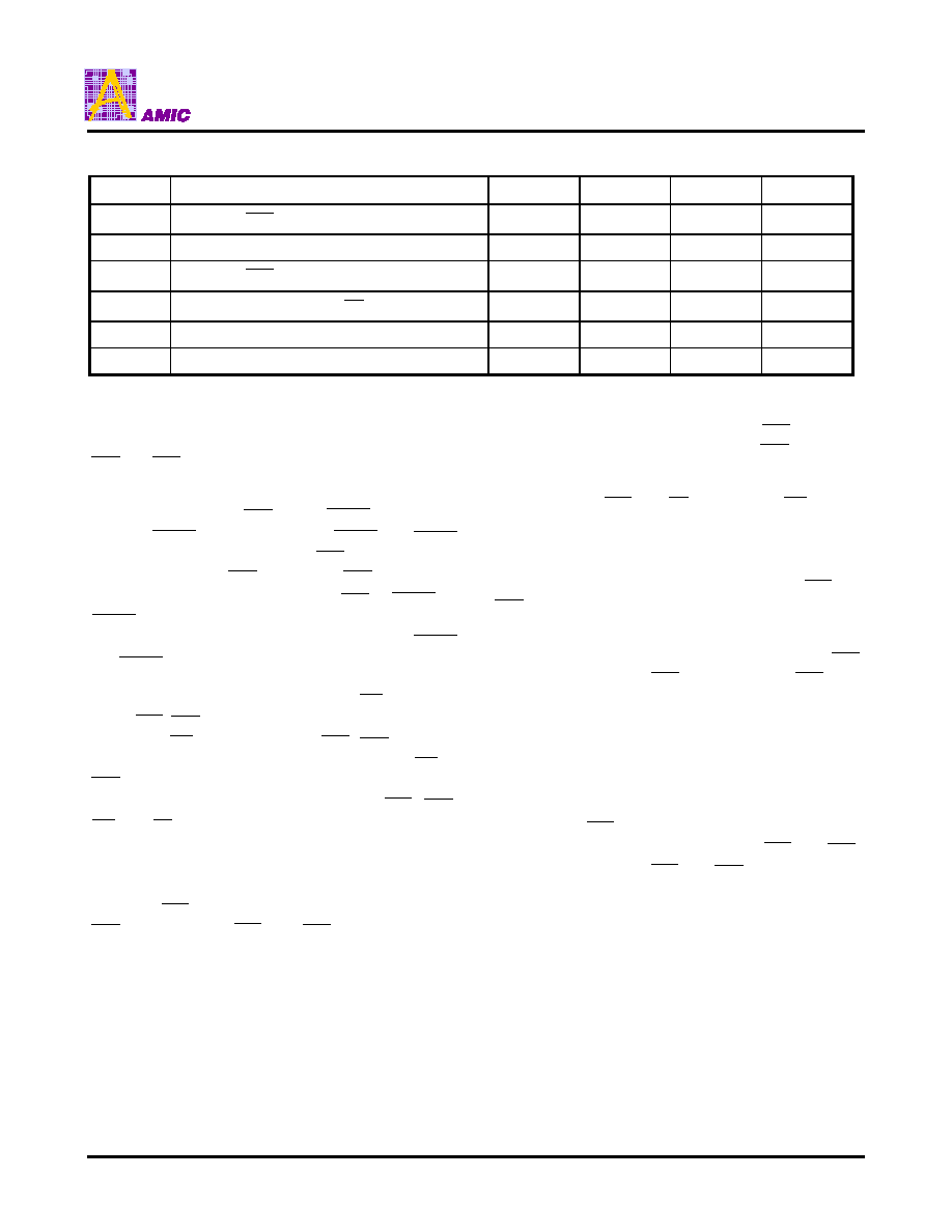
Word Read Cycle
t
RAS(3)
t
RP(2)
t
RC(1)
t
CRP(9)
t
CSH(8)
t
RCD(5)
t
RSH(7)
t
CAS(4)
t
ASR(10)
t
CRP(9)
t
RAH(11)
t
ASC(24)
t
CAH(25)
t
RAD(6)
t
RAL(20)
t
RCH(18)
t
RRH(19)
t
AR(16)
t
RCS(17)
t
ROH(51)
t
OEA(52)
t
RAC(13)
t
AA(15)
t
CAC(14)
t
CLZ(12)
t
OEZ(54)
t
OFF(23)
High-Z
: High or Low
Valid Data-out
Row Address
Column Address
I/O
0
~
I/O
15
OE
WE
Address
UCAS
LCAS
RAS
A42U0616 Series
PRELIMINARY (June, 2001, Version 0.0)
11
AMIC Technology, Inc.
Word Write Cycle (Early Write)
t
RAS(3)
t
RP(2)
t
RC(1)
t
CRP(9)
t
CSH(8)
t
RCD(5)
t
RSH(7)
t
CAS(4)
t
ASR(10)
t
CRP(9)
t
RAH(11)
t
ASC(24)
t
CAH(25)
t
RAD(6)
t
RAL(20)
t
WCH(28)
: High or Low
Row Address
Column Address
I/O
0
~
I/O
15
OE
Address
UCAS
LCAS
RAS
t
AR(16)
t
CWL(32)
t
RWL(31)
t
WP(30)
t
WCS(27)
Valid Data-in
t
DS(33)
t
DH(34)
WE
t
WCR(29)
t
DHR(35)
A42U0616 Series
PRELIMINARY (June, 2001, Version 0.0)
12
AMIC Technology, Inc.
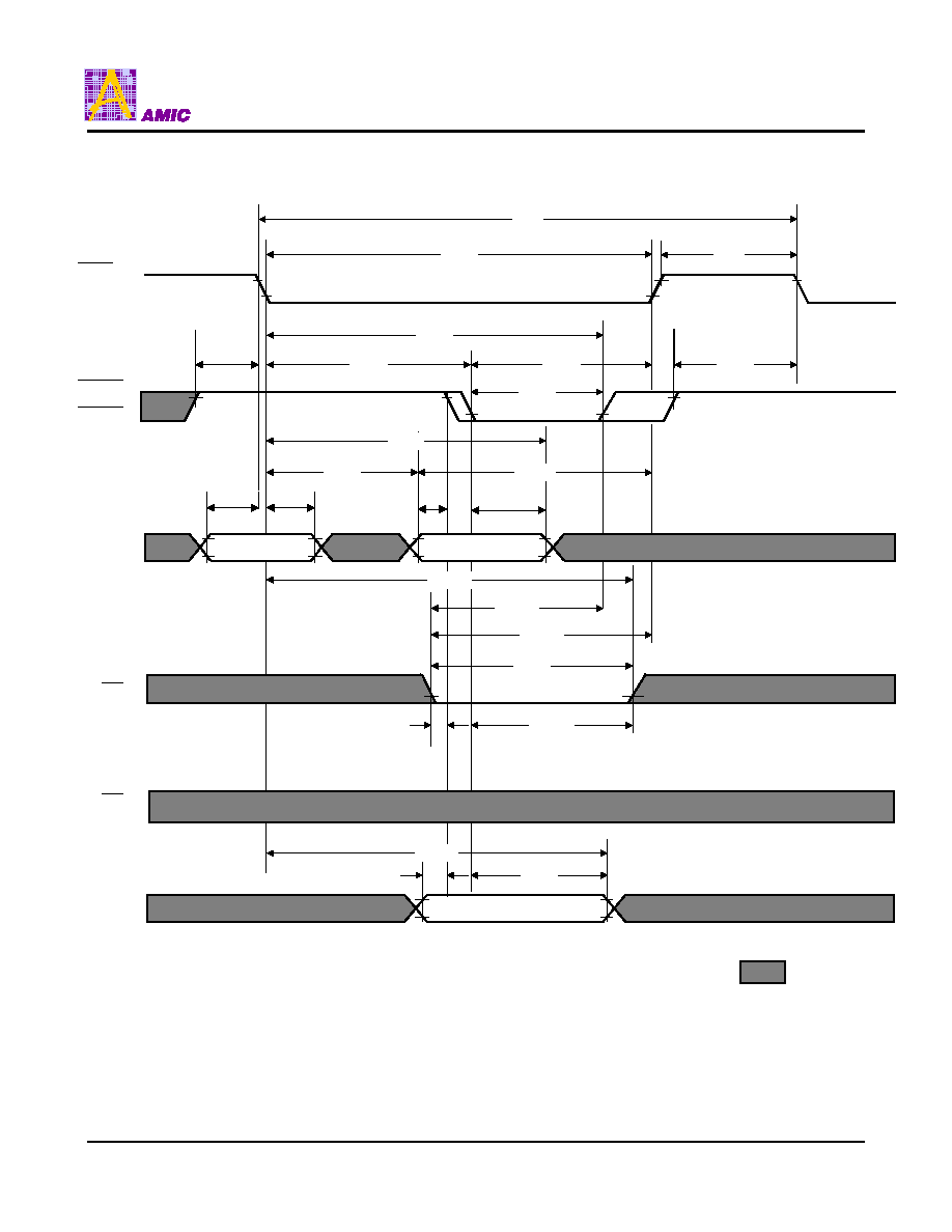
Word Write Cycle (
Late Write)
t
RAS(3)
t
RP(2)
t
RC(1)
t
CRP(9)
t
CSH(8)
t
RCD(5)
t
RSH(7)
t
CAS(4)
t
ASR(10)
t
CRP(9)
t
ASC(24)
t
CAH(25)
t
RAD(6)
t
RAL(20)
Row Address
Column Address
Address
UCAS
LCAS
RAS
t
AR(16)
t
CWL(32)
t
RWL(31)
t
WP(30)
t
RAH(11)
t
OEH(40)
t
OED(53)
t
DS(33)
t
DH(34)
I/O
0
~
I/O
15
: High or Low
OE
WE
High-Z
Vaild Data-in
t
WCR(29)
t
DHR(35)

A42U0616 Series
PRELIMINARY (June, 2001, Version 0.0)
13
AMIC Technology, Inc.
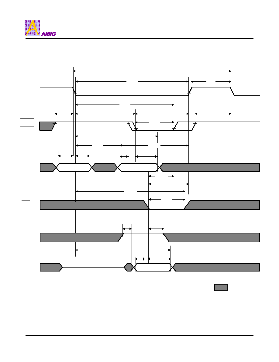
Word Read-Modify-Write Cycle
t
RAS(3)
t
RP(2)
t
RWC(36)
t
CRP(9)
t
CSH(8)
t
RCD(5)
t
RSH(7)
t
CAS(4)
t
ASR(10)
t
CRP(9)
t
RAH(11)
t
CAH(25)
t
RAD(6)
Row Address
Column Address
Address
UCAS
LCAS
RAS
t
AR(16)
t
RWL(31)
t
ASC(24)
t
CWL(32)
t
AWD(39)
t
CWD38)
t
RWD(37)
t
WP(30)
t
OEA(52)
t
OEZ(54)
t
CLZ(12)
t
CAC(14)
t
OED(53)
t
AA(15)
t
RAC(13)
t
DS(33)
t
DH(34)
High-Z
Data-out
Data-in
: High or Low
I/O
0
~
I/O
15
OE
WE
t
OEH(40)
t
RCS(17)

A42U0616 Series
PRELIMINARY (June, 2001, Version 0.0)
14
AMIC Technology, Inc.
EDO Page Mode Word Read Cycle
t
RASP(47)
t
RP(2)
RAS
UCAS
LCAS
t
CAS(4)
t
CAS(4)
t
CAS(4)
t
RCD(5)
t
CSH(8)
t
CRP(9)
t
CRP(9)
t
PC(42)
t
RSH(7)
t
ASR(10)
t
RAH(11)
t
RAD(6)
t
AR(16)
t
RAL(20)
Address
OE
WE
I/O
0
~
I/O
15
: High or Low
t
ASC(24)
t
CP(44)
t
CSH(8)
t
ASC(24)
t
CAH(25)
t
CAH(25)
Row
Column
Column
Column
t
RCH(25)
t
RCS(17)
t
RCS(17)
t
RCH(25)
t
RCS(17)
t
CAH(25)
t
RRH(19)
t
OFF(23)
t
OEZ(54)
t
AA(15)
t
OEA(52)
t
OEP(41)
t
CAC(14)
t
CLZ(12)
t
OEZ(54)
t
CPA(43)
t
OES(26)
t
AA(15)
t
OEA(52)
t
COH(21)
t
CAC(14)
t
RAC(13)
t
CAC(14)
t
CLZ(12)
Data-out
Data-out
Data-out

A42U0616 Series
PRELIMINARY (June, 2001, Version 0.0)
15
AMIC Technology, Inc.
EDO Page Mode Early Word Write Cycle
t
RASP(47)
t
RP(2)
RAS
UCAS
LCAS
t
CAS(4)
t
CP(44)
t
CAS(4)
t
CP(44)
t
CAS(4)
t
RCD(5)
t
CSH(8)
t
CRP(9)
t
CRP(9)
t
PC(42)
t
RSH(7)
t
ASR(10)
t
RAH(11)
t
RAD(6)
t
ASC(24)
t
CAH(25)
t
ASC(24)
t
CAH(25)
t
CAH(25)
t
ASC(24)
t
RAL(20)
Row
Column
Column
Address
WE
t
CWL(32)
t
WCH(28)
t
WCS(27)
t
WCS(27)
Column
t
CWL(32)
t
WCH(28)
t
WCS(27)
t
WCH(28)
t
CWL(32)
t
RWL(31)
t
WP(30)
t
WP(30)
t
WP(30)
t
DH(34)
t
DS(33)
t
DH(34)
t
DS(33)
t
DS(33)
t
DH(34)
Data-in
Data-in
Data-in
I/O
0
~
I/O
15
OE
: High or Low
A42U0616 Series
PRELIMINARY (June, 2001, Version 0.0)
16
AMIC Technology, Inc.
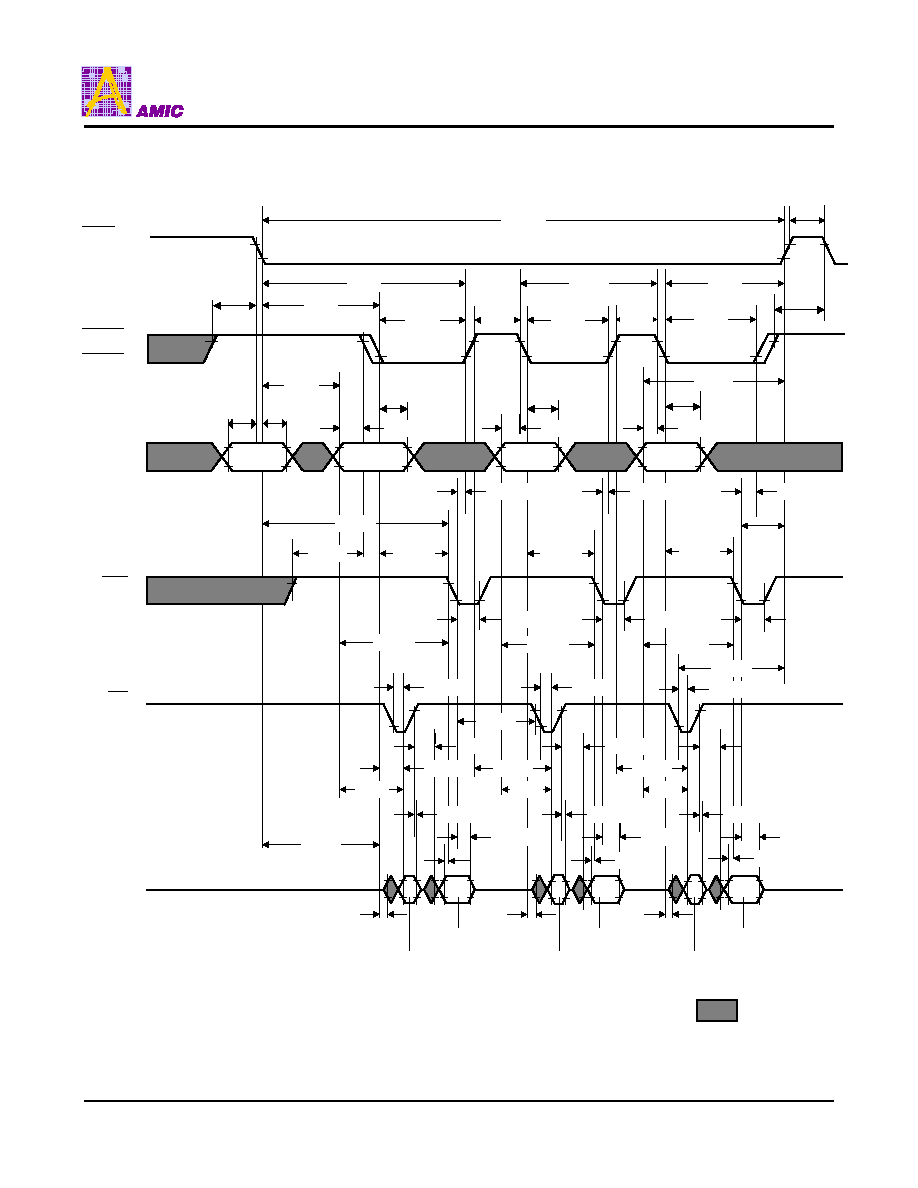
EDO Page Mode Word Read-Modify-Write Cycle
t
RASP(47)
RAS
t
CAS(4)
t
CP(44)
t
CAS(4)
t
CP(44)
t
CAS(4)
t
RCD(5)
t
CSH(8)
t
CRP(9)
t
CRP(9)
t
PCM(45)
t
RSH(7)
t
RP(2)
t
ASR(10)
t
RAH(11)
t
RAD(6)
t
ASC(24)
t
CAH(25)
t
ASC(24)
t
CAH(25)
t
ASC(24)
t
CAH(25)
t
RAL(20)
t
RCS(17)
t
CWD(38)
t
RWD(37)
t
CWL(32)
t
CWD(38)
t
CWL(32)
t
CWD(38)
t
CWL(32)
t
RWL(31)
t
OEA(52)
t
OEA(52)
t
OEA(52)
t
WP(30)
t
WP(30)
t
WP(30)
t
AWD(39)
t
AWD(39)
t
AWD(39)
t
ROH(51)
t
CAC(14)
t
AA(15)
t
RAC(13)
t
OED(53)
t
OEZ(54)
t
DS(33)
t
AA(15)
t
CPA(43)
t
DH(34)
t
OEZ(54)
t
OED(53)
t
DS(33)
t
DH(34)
t
OEZ(54)
t
DS(33)
t
OED(53)
t
DH(34)
t
AA(15)
t
CPA(43)
t
CLZ(12)
t
CLZ(12)
t
CLZ(12)
High-Z
: High or Low
I/O
0
~
I/O
15
OE
WE
Address
UCAS
LCAS
Data-out
Data-in
Data-out
Data-in
Data-out
Data-in
Row
Column
Column
Column
t
OEH(40)

A42U0616 Series
PRELIMINARY (June, 2001, Version 0.0)
17
AMIC Technology, Inc.
RAS
Only Refresh Cycle
CAS
Before
RAS
Refresh Cycle
t
RAS(3)
t
RP(2)
t
RC(1)
RAS
t
CRP(9)
t
RPC(50)
t
ASR(10)
t
RAH(11)
Address
UCAS
: High or Low
Row
Note: WE, OE = Don't care.
LCAS
t
RAS(3)
t
RP(2)
t
RC(1)
RAS
t
RP(2)
t
RPC(50)
t
PC(42)
t
CSR(48)
t
CHR(49)
t
OFF(23)
I/O
0
~
I/O
15
UCAS
High-Z
: High or Low
Note: WE, OE, Address = Don't care.
LCAS

A42U0616 Series
PRELIMINARY (June, 2001, Version 0.0)
18
AMIC Technology, Inc.
Hidden Refresh Cycle (Word Read)
t
RAS(3)
t
RP(2)
t
RC(1)
t
CRP(9)
t
AR(16)
t
RCD(5)
t
ASR(10)
t
CRP(9)
t
ASC(24)
t
CAH(25)
t
RAD(6)
Address
UCAS
RAS
t
RAH(11)
t
RRH(19)
t
RCS(17)
I/O
0
~
I/O
15
: High or Low
OE
High-Z
t
RAS(3)
t
RP(2)
t
CHR(49)
t
RC(1)
t
RSH(7)
t
RAL(20)
t
CAC(14)
t
OFF(23)
t
AA(15)
t
CLZ(12)
t
RAC(13)
WE
Row
Column
Valid Data-out
LCAS

A42U0616 Series
PRELIMINARY (June, 2001, Version 0.0)
19
AMIC Technology, Inc.
Hidden Refresh Cycle (Early Word Write)
t
RAS(3)
t
RP(2)
t
RC(1)
t
CRP(9)
t
AR(16)
t
RCD(5)
t
ASR(10)
t
CRP(9)
t
ASC(24)
t
CAH(25)
t
RAD(6)
Address
RAS
t
RAH(11)
: High or Low
OE
t
RAS(3)
t
RP(2)
t
CHR(49)
t
RC(1)
t
RSH(7)
t
RAL(20)
WE
Row
Column
t
WCS(27)
t
WCH(28)
t
WP(30)
t
DS(33)
t
DH(34)
Valid Data-in
I/O
0
~
I/O
15
UCAS
LCAS
A42U0616 Series
PRELIMINARY (June, 2001, Version 0.0)
20
AMIC Technology, Inc.
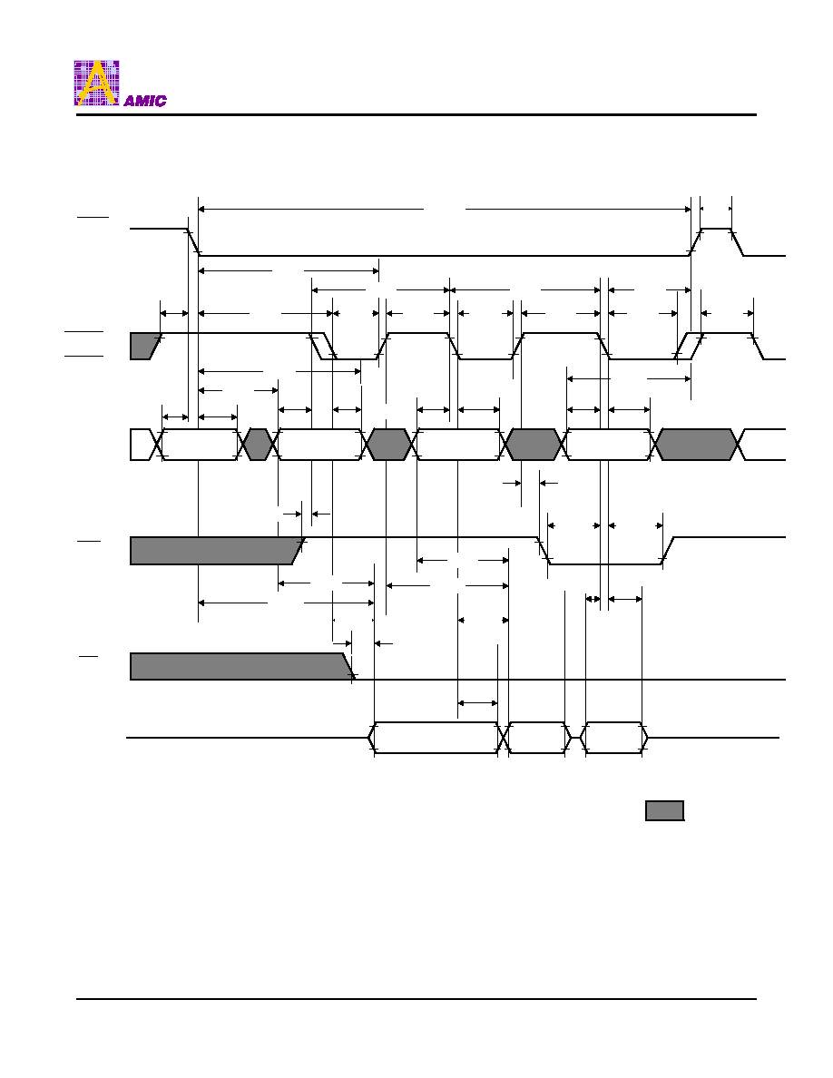
EDO Page Mode Read-Early-Write Cycle (Pseudo Read-Modify-Write)
RAS
: High or Low
I/O
0
~
I/O
15
OE
WE
Address
UCAS
t
RP(2)
t
RASP(47)
t
CRP(9)
t
CSH(8)
t
RCD(5)
t
CAS(4)
t
CP(44)
t
CAS(4)
t
CP(44)
t
CAS(4)
t
CPR(9)
t
RSH(7)
t
PC(42)
t
PC(42)
Row
Column
Column
t
RAL(20)
t
CAH(25)
t
ASC(24)
t
CAH(25)
t
ASC(24)
t
CAH(25)
t
ASC(24)
t
ASR(10)
t
RAH(11)
t
RAD(6)
t
RAD(6)
Column
t
RCS(17)
t
RCH(18)
t
WCS(27)
t
WCH(28)
Data-out
Data-out
Data-in
t
DH(34)
t
DS(33)
t
AA(15)
t
CAP(43)
t
CAC(14)
t
COH(21)
t
AA(15)
t
RAC(13)
t
CAC(14)
t
OEA(52)
LCAS

A42U0616 Series
PRELIMINARY (June, 2001, Version 0.0)
21
AMIC Technology, Inc.
Self Refresh Mode
n
Self Refresh Mode.
a. Entering the Self Refresh Mode:
The A42U0616 Self Refresh Mode is entered by using
CAS
before
RAS
cycle and holding
RAS
and
CAS
signal
"low" longer than 100
µ
s.
b. Continuing the Self Refresh Mode:
The Self Refresh Mode is continued by holding
RAS
"low" after entering the Self Refresh Mode.
It does not depend on
CAS
being "high" or "low" after entering the Self Refresh Mode continue the Self Refresh Mode.
c. Exiting the Self Refresh Mode:
The A42U0616 exits the Self Refresh Mode when the
RAS
signal is brought "high".
t
RASS(55)
t
RP(2)
t
CRP(9)
t
CSR(48)
t
RPC(50)
RAS
t
RPS(56)
t
CHS(57)
t
ASR(10)
t
CPN(42)
t
OFF(23)
A0 ~ A7
: High or Low
High-Z
I/O
0
~
I/O
15
UCAS
LCAS
ROW
COL
Note: WE, OE = Don't care.

A42U0616 Series
PRELIMINARY (June, 2001, Version 0.0)
22
AMIC Technology, Inc.
Capacitance
(Ta = Room Temperature, VCC = 2.5V
±
10%)
Symbol
Signals
Parameter
Max.
Unit
Test Conditions
C
IN1
A0 ≠ A9
5
pF
Vin = 0V
C
IN2
RAS
,
CAS
,
WE
,
OE
Input Capacitance
7
pF
Vin = 0V
C
I/O
I/O
0
- I/O
15
I/O Capacitance
10
pF
Vin = Vout = 0V
Ordering Codes
Package\ RAS Access Time
50ns
60ns
80ns
Refresh
Cycle
Self-
Refresh
42L SOJ (400mil)
A42U0616S-50
A42U0616S-60
A42U0616S-80
1K
Yes
50(44)L TSOP type II (400mil)
A42U0616V-50
A42U0616V-60
A42U0616V-80
1K
Yes
A42U0616 Series
PRELIMINARY (June, 2001, Version 0.0)
23
AMIC Technology, Inc.
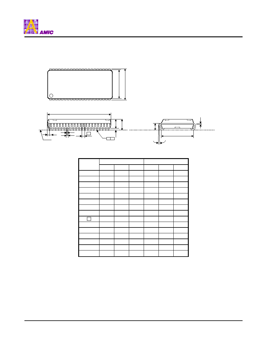
Package Information
SOJ 42L Outline Dimensions
unit: inches/mm
Dimensions in inches
Dimensions in mm
Symbol
Min
Nom
Max
Min
Nom
Max
A
0.128
0.138
0.148
3.25
3.51
3.76
A
1
0.025
-
-
0.64
-
-
A
2
0.105
0.110
0.115
2.67
2.79
2.92
b
1
0.026
0.028
0.032
0.66
0.71
0.81
b
0.015
0.018
0.020
0.38
0.46
0.51
C
0.007
0.008
0.013
0.18
0.20
0.33
D
1.075
1.080
1.085
27.31
27.43
27.56
E
0.395
0.400
0.405
10.03
10.16
10.29
e
-
0.050
-
-
1.27
-
e
1
-
0.370
-
-
9.4
-
H
E
0.435
0.440
0.445
11.05
11.18
11.30
L
0.082
-
-
2.08
-
-
S
-
-
0.045
-
-
1.14
y
-
-
0.003
-
-
0.075
0
∞
-
10
∞
0
∞
-
10
∞
Notes:
1. The maximum value of dimension D includes end flash.
2. Dimension E does not include resin fins.
3. Dimension e
1
is for PC Board surface mount pad pitch design
reference only.
4. Dimension S includes end flash.
1
E
H
E
21
22
42
A
1
A
2
e
e
1
C
S
D
Seating Plane
D y
L
1
A
b
b

A42U0616 Series
PRELIMINARY
(June, 2001, Version 0.0)
24
AMIC Technology, Inc.
Package Information
TSOP 50/44L (Type II) Outline Dimensions
unit: inches/mm
1
E
H
E
L
1
c
50
A
1
A
2
A
S
D y
e
D
B
L
Detail "A"
Detail "A"
25
26
Seating Plane
RAD R1
RAD R
Dimensions in inches
Dimensions in mm
Symbol
Min
Nom
Max
Min
Nom
Max
A
-
-
0.048
-
-
1.20
A
1
0.002
-
0.006
0.05
-
0.15
A
2
0.037
0.039
0.042
0.95
1.00
1.05
B
0.012
-
0.018
0.30
-
0.45
c
0.005
-
0.008
0.12
-
0.21
D
0.820
0.825
0.830
20.82
20.95
21.08
E
0.400 BSC
10.16 BSC
H
E
0.463 BSC
11.76 BSC
L
0.016
0.020
0.024
0.40
0.50
0.60
L
1
0.031 REF
0.80 REF
e
0.031 BSC
0.80 BSC
R
0.005
-
0.010
0.12
-
0.25
R
1
0.005
-
-
0.12
-
-
S
0.0435 REF
0.875 BSC
0∞
-
5∞
0∞
-
5∞
Notes:
1. The maximum value of dimension D includes end flash.
2. Dimension E does not include resin fins.
3. Dimension S includes end flash.