
A43L0616B
Preliminary
512K X 16 Bit X 2 Banks Synchronous DRAM
PRELIMINARY (May, 2005, Version 0.0)
AMIC Technology, Corp.
Document Title
512K X 16 Bit X 2 Banks Synchronous DRAM
Revision History
Rev. No. History Issue
Date Remark
0.0
Initial issue
May 10, 2005
Preliminary
A43L0616B
Preliminary
512K X 16 Bit X 2 Banks Synchronous DRAM
PRELIMINARY (May, 2005, Version 0.0)
1
AMIC Technology, Corp.
Features
JEDEC standard 3.3V power supply
LVTTL compatible with multiplexed address
Dual banks / Pulse
RAS
MRS cycle with address key programs
- CAS Latency (2,3)
- Burst Length (1,2,4,8 & full page)
-
Burst Type (Sequential & Interleave)
All inputs are sampled at the positive going edge of the
system clock
Industrial operating temperature range: -40∫C to +85∫C
for ≠U
Pb-Free type for -F
Burst Read Single-bit Write operation
DQM for masking
Auto & self refresh
32ms refresh period (2K cycle)
50 Pin TSOP (II)
General Description
The A43L0616B is 16,777,216 bits synchronous high data
rate Dynamic RAM organized as 2 X 524,288 words by 16
bits, fabricated with AMIC's high performance CMOS
technology. Synchronous design allows precise cycle control
with the use of system clock. I/O transactions are possible on
every clock cycle. Range of operating frequencies,
programmable latencies allows the same device to be useful
for a variety of high bandwidth, high performance memory
system applications.
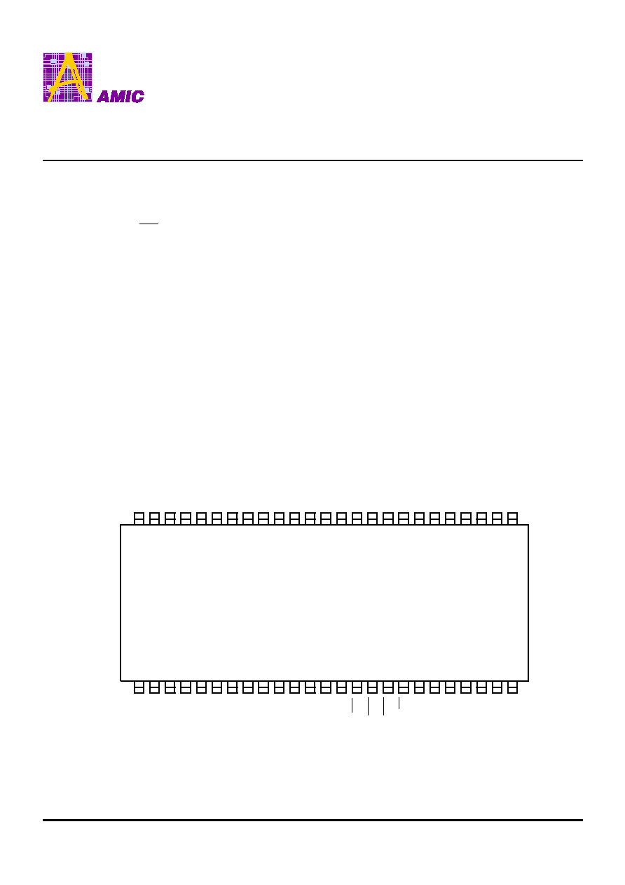
Pin Configuration
TSOP (II)
A43L0616
BV
50 49 48 47 46 45 44 43 42 41
39
40
38 37 36 35 34 33 32 31 30 29 28 27 26
1
2
3
4 5
6
7
8
9 10
12
11
13 14 15 16 17 18 19 20 21 22 23 24 25
VSS
DQ
15
DQ
14
VSSQ
DQ
13
DQ
12
VDDQ
DQ
11
DQ
10
VSSQ
DQ
9
DQ
8
VDDQ
NC/RFU
UDQM
CLK
CKE
NC
A9
A8
A7
A6
A5
A4
VSS
VDD
DQ
0
DQ
1
VSSQ
DQ
2
DQ
3
VDDQ
DQ
4
DQ
5
VSSQ
DQ
6
DQ
7
VDDQ
LDQM
WE
CAS
RAS
CS
BA
A10/AP
A0
A1
A2
A3
VDD
A43L0616B
PRELIMINARY (May, 2005, Version 0.0)
2
AMIC Technology, Corp.
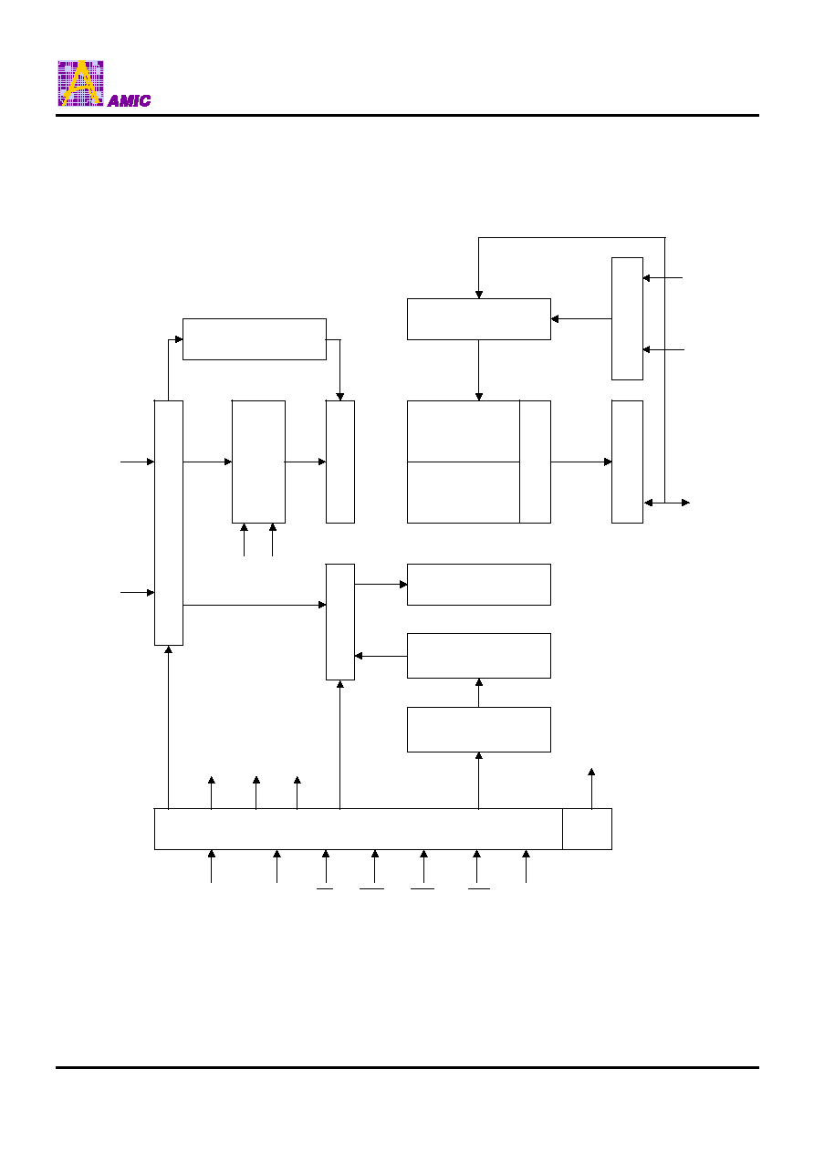
Block Diagram
Bank Select
Row Buffer
Ref
r
esh Count
er
Address Regi
st
er
Row Decoder
Co
lu
mn
Bu
ffe
r
LCBR
LRAS
CLK
ADD
Timing Register
Data Input Register
512K X 16
512K X 16
Sense AMP
Column Decoder
Latency & Burst Length
Programming Register
LRAS
LCAS
LRAS
LCBR
LWE
LWCBR
LDQM
CLK
CKE
CS
RAS
CAS
WE
L(U)DQM
I/O Co
n
t
ro
l
Ou
tp
u
t
Bu
ffe
r
LWE
LDQM
DQi

A43L0616B
PRELIMINARY (May, 2005, Version 0.0)
3
AMIC Technology, Corp.
Pin Descriptions
Symbol Name
Description
CLK
System Clock
Active on the positive going edge to sample all inputs.
CS
Chip Select
Disables or Enables device operation by masking or enabling all inputs except CLK,
CKE and L(U)DQM
CKE Clock
Enable
Masks system clock to freeze operation from the next clock cycle.
CKE should be enabled at least one clock + tss prior to new command.
Disable input buffers for power down in standby.
A0~A10/AP Address
Row / Column addresses are multiplexed on the same pins.
Row address : RA0~RA10, Column address: CA0~CA7
BA
Bank Select Address
Selects bank to be activated during row address latch time.
Selects band for read/write during column address latch time.
RAS
Row Address Strobe
Latches row addresses on the positive going edge of the CLK with RAS low.
Enables row access & precharge.
CAS
Column Address
Strobe
Latches column addresses on the positive going edge of the CLK with CAS low.
Enables column access.
WE
Write Enable
Enables write operation and Row precharge.
L(U)DQM
Data Input/Output
Mask
Makes data output Hi-Z, t SHZ after the clock and masks the output.
Blocks data input when L(U)DQM active.
DQ
0-15
Data Input/Output
Data inputs/outputs are multiplexed on the same pins.
VDD/VSS
Power
Supply/Ground
Power Supply: +3.3V
±
0.3V/Ground
VDDQ/VSSQ
Data Output
Power/Ground
Provide isolated Power/Ground to DQs for improved noise immunity.
NC/RFU No
Connection
A43L0616B
PRELIMINARY (May, 2005, Version 0.0)
4
AMIC Technology, Corp.
Absolute Maximum Ratings*
Voltage on any pin relative to VSS (Vin, Vout ) . . . . . . . . .
. . . . . . . . . . . . . . . . . . . . . . . . . . . . . . . . . . -1.0V to +4.6V
Voltage on VDD supply relative to VSS (VDD, VDDQ )
. . . . . . . . . . . . . . . . . . . . . . . . . . . . . . . . . . -1.0V to +4.6V
Storage Temperature (T
STG
) . . . . . . . . . . -55
∞
C to +150
∞
C
Soldering Temperature X Time (T
SLODER
) . . . . . . . . . . . . . .
. . . . . . . . . . . . . . . . . . . . . . . . . . . . . . . . . . 260
∞
C X 10sec
Power Dissipation (P
D
) . . . . . . . . . . . . . . . . . . . . . . . . . 1W
Short Circuit Current (Ios) . . . . . . . . . . . . . . . . . . . . 50mA
*Comments
Permanent device damage may occur if "Absolute Maximum
Ratings" are exceeded.
Functional operation should be restricted to recommended
operating condition.
Exposure to higher than recommended voltage for extended
periods of time could affect device reliability.
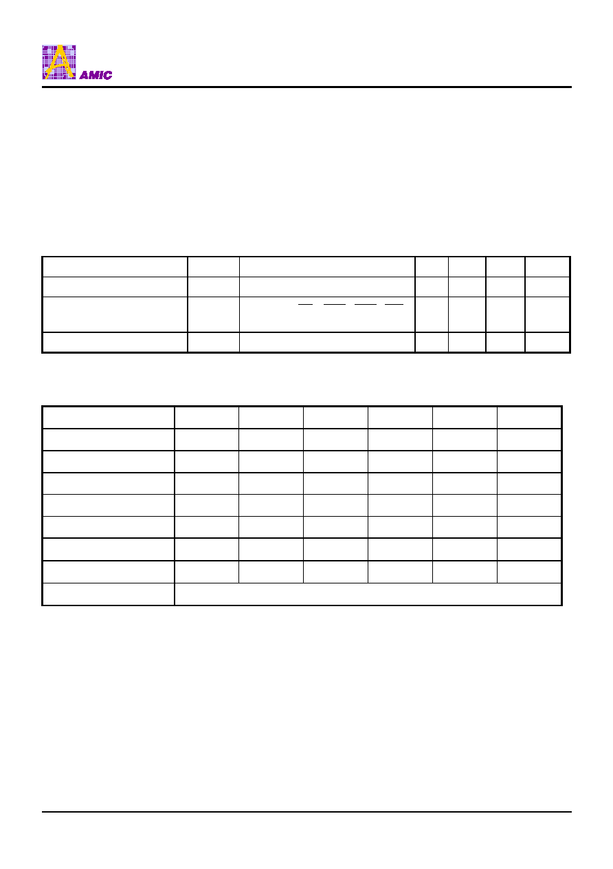
Capacitance (T
A
=25
∞
C, f=1MHz)
Parameter Symbol
Condition
Min
Typ
Max
Unit
Input Capacitance
CI1
A0 to A10, BA
2
4
pF
CI2
CLK, CKE,
CS
,
RAS
,
CAS
,
WE
,
UDQM, LDQM
2 4 pF
Data Input/Output Capacitance
CI/O
DQ0 to DQ15
2
6
pF
DC Electrical Characteristics
Recommend operating conditions (Voltage referenced to VSS = 0V, T
A
= 0∫C to +70∫C or -40∫C to +85∫C)
Parameter Symbol
Min
Typ
Max
Unit
Note
Supply
Voltage
VDD,VDDQ
3.0 3.3 3.6 V
Input High Voltage
V
IH
2.0 3.0
VDD+0.3
V
Input Low Voltage
V
IL
-0.3 0 0.8 V Note
1
Output High Voltage
V
OH
2.4 -
- V
I
OH
= -2mA
Output Low Voltage
V
OL
- - 0.4 V
I
OL
= 2mA
Input Leakage Current
I
IL
-5 - 5
µ
A
Note 2
Output Leakage Current
I
OL
-5 - 5
µ
A
Note 3
Output Loading Condition
See Figure 1
Note:
1. V
IL
(min) = -1.5V AC (pulse width
5ns).
2. Any input 0V
VIN
VDD + 0.3V, all other pins are not under test = 0V
3. Dout is disabled, 0V
Vout
VDD