Äîêóìåíòàöèÿ è îïèñàíèÿ www.docs.chipfind.ru
A43L0632
Preliminary
512K X 32 Bit X 2 Banks Synchronous DRAM
PRELIMINARY (August, 2005, Version 0.0)
AMIC Technology, Corp.
Document Title
512K X 32 Bit X 2 Banks Synchronous DRAM
Revision History
Rev. No. History Issue
Date Remark
0.0
Initial issue
August 1, 2005
Preliminary
A43L0632
Preliminary
512K X 32 Bit X 2 Banks Synchronous DRAM
PRELIMINARY (August, 2005, Version 0.0)
1
AMIC Technology, Corp.
Features
Power supply
- VDD: 3.3V VDDQ : 3.3V
LVTTL compatible with multiplexed address
Two banks / Pulse
RAS
MRS cycle with address key programs
- CAS Latency (2 & 3)
- Burst Length (1,2,4,8 & full page)
-
Burst Type (Sequential & Interleave)
Clock Frequency (max) : 167MHz @ CL=3 (-6)
143MHz @ CL=3 (-7)
All inputs are sampled at the positive going edge of the
system clock
DQM for masking
Auto & self refresh
64ms refresh period (4K cycle)
Industrial operating temperature range: -40ºC to +85ºC
for -U series.
Available in 90 Balls CSP (8mm X 13mm)
Package is available to lead free (-F series)
General Description
The A43L0632 is 33,554,432 bits synchronous high data
rate Dynamic RAM organized as 2 X 524,288 words by 32
bits, fabricated with AMIC's high performance CMOS
technology. Synchronous design allows precise cycle
control with the use of system clock. I/O transactions are
possible on every clock cycle. Range of operating
frequencies, programmable latencies allows the same
device to be useful for a variety of high bandwidth, high
performance memory system applications.
Pin Configuration
90 Balls CSP (8 mm x 13 mm)
Top View
90 Ball (8X13) CSP
1 2 3
7
8
9
A DQ
26
DQ
24
VSS
VDD
DQ
23
DQ
21
B DQ
28
VDDQ
VSSQ
VDDQ
VSSQ
DQ
19
C VSSQ
DQ
27
DQ
25
DQ
22
DQ
20
VDDQ
D VSSQ
DQ
29
DQ
30
DQ
17
DQ
18
VDDQ
E VDDQ
DQ
31
NC
NC
DQ
16
VSSQ
F VSS
DQM
3
A3
A2
DQM
2
VDD
G
A4
A5
A6
A10
A0
A1
H
A7
A8
NC
NC
NC
NC
J CLK
CKE A9 BA
CS
RAS
K DQM
1
NC NC
CAS
WE
DQM
0
L VDDQ
DQ
8
VSS
VDD
DQ
7
VSSQ
M
VSSQ
DQ
10
DQ
9
DQ
6
DQ
5
VDDQ
N VSSQ
DQ
12
DQ
14
DQ
1
DQ
3
VDDQ
P DQ
11
VDDQ
VSSQ
VDDQ
VSSQ
DQ
4
R DQ
13
DQ
15
VSS
VDD
DQ
0
DQ
2
A43L0632
PRELIMINARY (August, 2005, Version 0.0)
2
AMIC Technology, Corp.
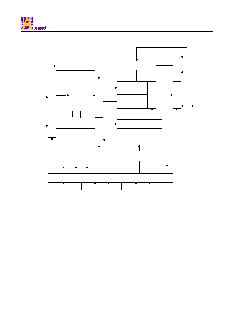
Block Diagram
Bank Select
Ro
w
B
u
f
f
e
r
Ref
r
e
s
h Cou
n
te
r
A
ddr
ess
Reg
i
s
t
e
r
Row D
e
c
ode
r
Col
u
mn Buff
e
r
LCBR
LRAS
CLK
ADD
Timing Register
Data Input Register
512K X 32
Sen
s
e
AMP
Column Decoder
Latency & Burst Length
Programming Register
LRAS
LCAS
LRAS
LCBR
LWE
LWCBR
DQM
CLK
CKE
CS
RAS
CAS
WE
DQM
I/O
C
o
nt
ro
l
Ou
tp
u
t
B
u
f
f
e
r
LWE
DQM
DQi
512K X 32
A43L0632
PRELIMINARY (August, 2005, Version 0.0)
3
AMIC Technology, Corp.
Pin Descriptions
Symbol Name
Description
CLK
System Clock
Active on the positive going edge to sample all inputs.
CS
Chip Select
Disables or Enables device operation by masking or enabling all inputs except
CLK, CKE and DQM
CKE Clock
Enable
Masks system clock to freeze operation from the next clock cycle.
CKE should be enabled at least one clock + tss prior to new command.
Disable input buffers for power down in standby.
A0~A10 Address
Row / Column addresses are multiplexed on the same pins.
Row address : RA0~RA10, Column address: CA0~CA7
BA
Bank Select Address
Selects bank to be activated during row address latch time.
Selects band for read/write during column address latch time.
RAS
Row Address Strobe
Latches row addresses on the positive going edge of the CLK with RAS low.
Enables row access & precharge.
CAS
Column Address
Strobe
Latches column addresses on the positive going edge of the CLK with CAS low.
Enables column access.
WE
Write Enable
Enables write operation and Row precharge.
DQMi
Data Input/Output
Mask
Makes data output Hi-Z, t SHZ after the clock and masks the output.
Blocks data input when DQM active.
DQ
0-31
Data Input/Output
Data inputs/outputs are multiplexed on the same pins.
VDD/VSS
Power
Supply/Ground
Power Supply: +3.3V
±
0.3V/Ground
VDDQ/VSSQ
Data Output
Power/Ground
Provide isolated Power/Ground to DQs for improved noise immunity.
NC/RFU No
Connection

A43L0632
PRELIMINARY (August, 2005, Version 0.0)
4
AMIC Technology, Corp.
Absolute Maximum Ratings*
Voltage on any pin relative to VSS (Vin, Vout ) . . . . . . . . .
. . . . . . . . . . . . . . . . . . . . . . . . . . . . . . . . . . -1.0V to +4.6V
Voltage on VDD supply relative to VSS (VDD, VDDQ )
. . . . . . . . . . . . . . . . . . . . . . . . . . . . . . . . . . .-1.0V to + 4.6V
Storage Temperature (T
STG
) . . . . . . . . . . -55
°
C to +150
°
C
Soldering Temperature X Time (T
SLODER
) . . . . . . . . . . . . . .
. . . . . . . . . . . . . . . . . . . . . . . . . . . . . . . . . . 260
°
C X 10sec
Power Dissipation (P
D
) . . . . . . . . . . . . . . . . . . . . . . . . 0.8W
Short Circuit Current (Ios) . . . . . . . . . . . . . . . . . . . . 50mA
*Comments
Permanent device damage may occur if "Absolute
Maximum Ratings" are exceeded.
Functional operation should be restricted to recommended
operating condition.
Exposure to higher than recommended voltage for
extended periods of time could affect device reliability.
Capacitance (T
A
=25
°
C, f=1MHz)
Parameter Symbol
Condition
Min
Max
Unit
Input Capacitance
CI1
A0 to A10, BA
2.5
3.8
pF
CI2
CLK, CKE,
CS
,
RAS
,
CAS
,
WE
, DQM
2.5 3.8 pF
Data Input/Output Capacitance
CI/O
DQ
0
to DQ
31
4.0
6.5
pF
DC Electrical Characteristics
Recommend operating conditions
(Voltage referenced to VSS=0V, T
A
= 0ºC to +70ºC for commercial or T
A
=-40ºC to +85ºC for extended)
Parameter Symbol
Min
Typ
Max
Unit
Note
Supply Voltage
VDD
3
3.3
3.6
V
DQ Supply Voltage
VDDQ
3
3.3
3.6
V
Input High Voltage
V
IH
2 3
VDD+0.3
V
Input Low Voltage
V
IL
-0.3 - 0.8 V Note
1
Output High Voltage
V
OH
2.4 -
- V
I
OH
= -0.1mA
Output Low Voltage
V
OL
- - 0.4 V
I
OL
= 0.1mA
Input Leakage Current
I
IL
-5 - 5
µ
A
Note 2
Output Leakage Current
I
OL
-5 - 5
µ
A
Note 3
Output Loading Condition
See Fig. 1 (Page 6)
Note:
1. V
IL
(min) = -1.5V AC (pulse width
5ns).
2. Any input 0V
VIN
VDD + 0.3V, all other pins are not under test = 0V
3. Dout is disabled, 0V
Vout
VDD