
A45L9332A Series
Preliminary
256K X 32 Bit X 2 Banks Synchronous Graphic RAM
PRELIMINARY (October, 2001, Version 0.1)
AMIC Technology, Inc.
Document Title
256K X 32Bit X 2 Banks Synchronous Graphic RAM
Revision History
Rev. No. History
Issue Date
Remark
0.0
Initial issue
August 21, 2001
Preliminary
0.1
Update AC and DC data specification
October 22, 2001

A45L9332A Series
Preliminary
256K X 32 Bit X 2 Banks Synchronous Graphic RAM
PRELIMINARY (October, 2001, Version 0.1)
1
AMIC Technology, Inc.
Features
n
JEDEC standard 3.3V power supply
n
LVTTL compatible with multiplexed address
n
Dual banks / Pulse RAS
n
MRS cycle with address key programs
- CAS Latency (2,3)
- Burst Length (1,2,4,8 & full page)
-
Burst Type (Sequential & Interleave)
n
All inputs are sampled at the positive going edge of the
system clock
n
Burst Read Single-bit Write operation
n
DQM 0-3 for byte masking
n
Auto & self refresh
n
32ms refresh period (2K cycle)
n
100 Pin QFP, LQFP (14 X 20 mm)
Graphics Features
n
SMRS cycle
- Load mask register
- Load color register
n
Write Per Bit (Old Mask)
n
Block Write (8 Columns)
General Description
The A45L9332A is 16,777,216 bits synchronous high data
rate Dynamic RAM organized as 2 X 262,144 words by 32
bits, fabricated with AMIC's high performance CMOS
technology. Synchronous design allows precise cycle
control with the use of system clock. I/O transactions are
possible on every clock cycle. Range of operating
frequencies, programmable latencies allows the same
device to be useful for a variety of high bandwidth, high
performance memory system applications.
Write per bit and 8 columns block write improves
performance in graphics system.

A45L9332A Series
PRELIMINARY
(October, 2001, Version 0.1)
2
AMIC Technology, Inc.
Pin Configuration
VDDQ
DQ
20
DQ
21
DQ
22
DQ
23
DQM
0
BA(A10)
A8
1
2
3
4
5
6
7
8
9
10
11
12
13
14
15
16
17
18
19
20
21
22
23
24
25
26
28
30
27
29
80
79
78
77
76
75
74
72
73
71
70
69
68
67
66
65
64
63
62
61
60
59
58
57
56
55
54
53
52
51
VDDQ
VSSQ
DQ
25
DQ
24
VDDQ
DQ
15
DQ
14
VSSQ
VDDQ
VSS
VDD
DQ
11
DQ
10
VSSQ
DQ
9
DQ
8
VDDQ
NC
DQM
3
CKE
DSF
NC
A9
50
49
48
47
46
45
44
43
42
40
41
39
38
37
36
35
34
33
32
31
A7
A6
A5
A4
VSS
VDD
A3
A1
A0
81
82
83
84
85
86
87
88
89
90
91
92
93
94
95
96
97
98
99
100
VSSQ
DQ
2
VSSQ
A45L9332AE
A45L9332AF
VDDQ
NC
VSS
VSSQ
VDDQ
VSSQ
VDD
VSS
VSSQ
VDDQ
DQM
2
WE
CAS
RAS
CS
DQ
1
DQ
0
VDD
NC
NC
NC
NC
NC
NC
NC
NC
NC
DQ
31
DQ
30
DQ
29
A2
NC
NC
NC
NC
NC
NC
NC
NC
NC
NC
DQ
13
DQ
12
DQM
1
CLK
DQ
27
DQ
26
DQ
28
DQ
3
DQ
4
DQ
5
DQ
6
DQ
7
DQ
16
DQ
17
DQ
18
DQ
19
A45L9332A Series
PRELIMINARY
(October, 2001, Version 0.1)
3
AMIC Technology, Inc.
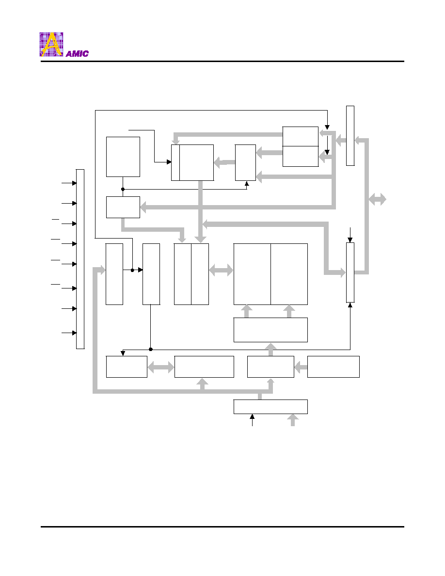
Block Diagram
(i=0~31)
BLOCK
WRITE
CONTROL
LOGIC
MASK
WRITE
CONTROL
LOGIC
MUX
MASK
REGISTER
CLOCK
REGISTER
INPUT BUFFER
TIMMING REGISTER
COLUMN
MASK
DQMi
INPUT BUFFER
PROGRAMING
REGISTER
LATENCY &
BURST LENGTH
COLUMN
DECORDER
SENSE AMPLIFIER
256K x 32
CELL
ARRAY
256K x 32
CELL
ARRAY
DQi
DQMi
ROW DECORDER
BANK SELECTION
SERIAL
COUNTER
COLUMN ADDRESS
BUFFER
ROW
ADDRESS
BUFFER
REFRESH
COUNTER
ADDRESS REGISTER
CLOCK
ADDRESS (A0~A10)
CLK
CKE
CS
RAS
CAS
WE
DSF
DQMi

A45L9332A Series
PRELIMINARY
(October, 2001, Version 0.1)
4
AMIC Technology, Inc.
Pin Descriptions
Symbol
Name
Description
CLK
System Clock
Active on the positive going edge to sample all inputs.
CS
Chip Select
Disables or Enables device operation by masking or enabling all inputs except
CLK, CKE and DQMi
CKE
Clock Enable
Masks system clock to freeze operation from the next clock cycle.
CKE should be enabled at least one clock + t ss prior to new command.
Disable input buffers for power down in standby.
A0~A9
Address
Row / Column addresses are multiplexed on the same pins.
Row address : RA0~RA9, Column address: CA0~CA7
A10(BA)
Bank Select Address
Selects bank to be activated during row address latch time.
Selects band for read/write during column address latch time.
RAS
Row Address Strobe
Latches row addresses on the positive going edge of the CLK with RAS low.
Enables row access & precharge.
CAS
Column Address Strobe
Latches column addresses on the positive going edge of the CLK with CAS low.
Enables column access.
WE
Write Enable
Enables write operation and Row precharge.
DQMi
Data Input/Output Mask
Makes data output Hi-Z, t SHZ after the clock and masks the output.
Blocks data input when DQM active. (Byte Masking)
DQi
Data Input/Output
Data inputs/outputs are multiplexed on the same pins.
DSF
Define Special Function
Enables write per bit, block write and special mode register set.
VDD/VSS
Power Supply/Ground
Power Supply: +3.3V
±
0.3V/Ground
VDDQ/VS
SQ
Data Output
Power/Ground
Provide isolated Power/Ground to DQs for improved noise immunity.
NC
No Connection