A61L6316 Series
64K X 16 BIT HIGH SPEED CMOS SRAM
(July, 2002, Version 1.1)
AMIC Technology, Inc.
Document Title
64K X 16 BIT HIGH SPEED CMOS SRAM
Revision History
Rev. No. History
Issue Date
Remark
0.0
Initial issue
July 14, 2000
Preliminary
1.0
Final spec. release
May 8, 2001
Final
Add -10 spec.
Change I
CC1
from 120mA to 220mA (-12)
Change I
CC1
from 100mA to 210mA (-15)
Change I
SB1
from 8mA to 12mA
Change I
CDR
from 1mA to 5mA
Add t
BE
, t
BLZ
, t
BHZ
, t
BW
parameters
1.1
Add -25
�
C ~ +85
�
C grade
July 17, 2002
A61L6316 Series
64K X 16 BIT HIGH SPEED CMOS SRAM
(July, 2002, Version 1.1)
1
AMIC Technology, Inc.
Features
General Description
n
Center power pinout
n
Supply voltage: -10: 3.3V+10%, -5%
-12, -15: 3.3V�10%
n
Access times: 10/12/15 ns (max.)
n
Current: Operating: -10: 230mA (max)
-12: 220mA (max.)
-15: 210mA (max.)
Standby: TTL: 25mA (max.)
CMOS: 12mA (max.)
n
Extended operating temperature range: -25
�
C to 85
�
C
for -I series
n
Full static operation, no clock or refreshing required
n
All inputs and outputs are directly TTL-compatible
n
Common I/O using three-state output
n
Data retention voltage: 2V (min.)
n
Available in 44-pin 400mil SOJ and 44-pin 400mil
TSOP(II) forward packages.
The A61L6316 is a high speed 1,048,576-bit static
random access memory organized as 65,536 words by 16
bits and operates on low power supply voltage from 3.0V
to 3.6V. It is built using AMIC's high performance CMOS
process.
Inputs and three-state outputs are TTL compatible and
allow for direct interfacing with common system bus
structures.
The chip enable input is provided for POWER-DOWN, to
disable the device. Two byte enable inputs and an output
enable input are included for easy interfacing.
Data retention is guaranteed at a power supply voltage as
low as 2V.
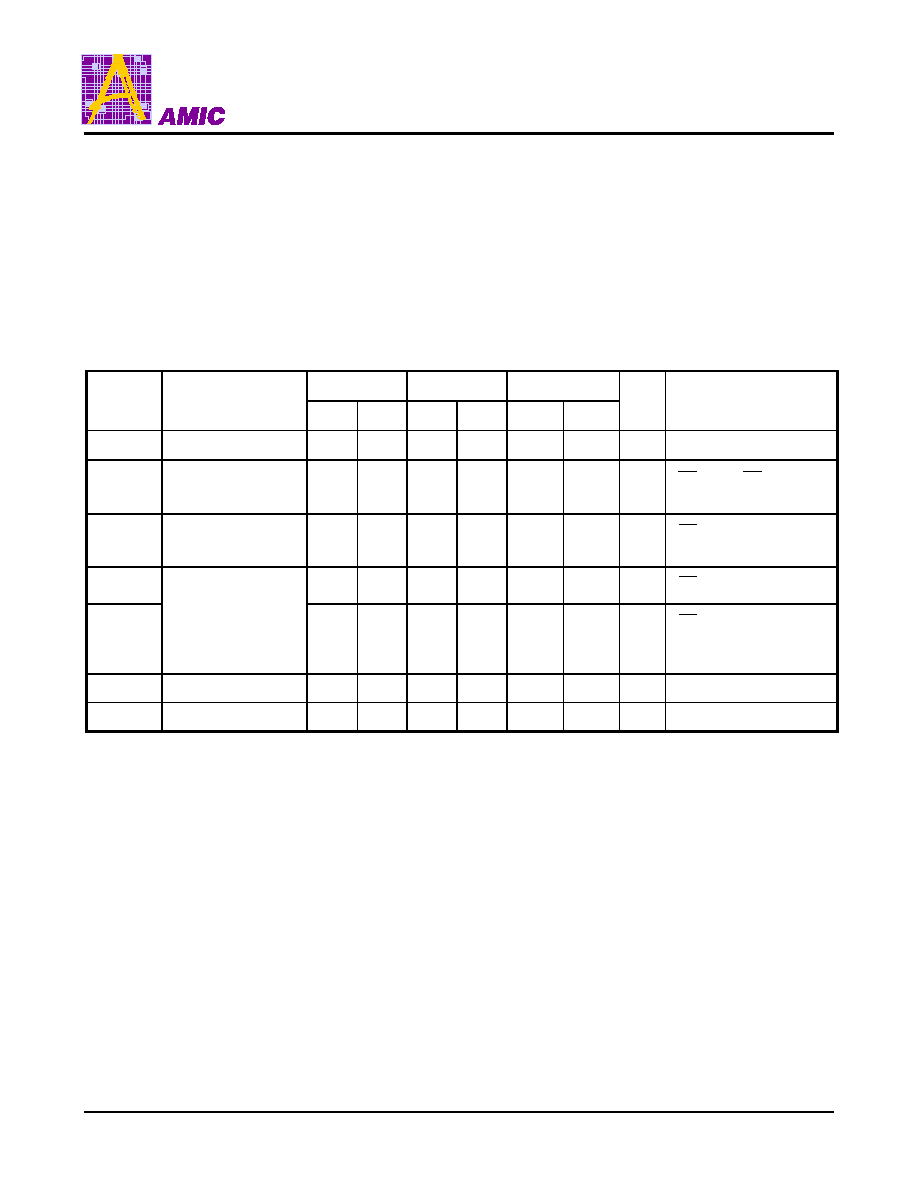
Product Family
Power Dissipation
Product
Family
Operating
Temperature
VCC Range
Speed
Data Retention
(I
CCDR
, Typ.)
Standby
(I
SB1
, Typ.)
Package
Type
A61L6316
0
�
C ~ +70
�
C
-25
�
C ~ +85
�
C
3.0V ~ 3.6V
10/12/15 ns
3mA
5mA
44L SOP
44L TSOP(II)
1. Typical values are measured at VCC = 3.3V, T
A
= 25
�
C and not 100% tested.
2. Data retention current VCC = 2.0V.
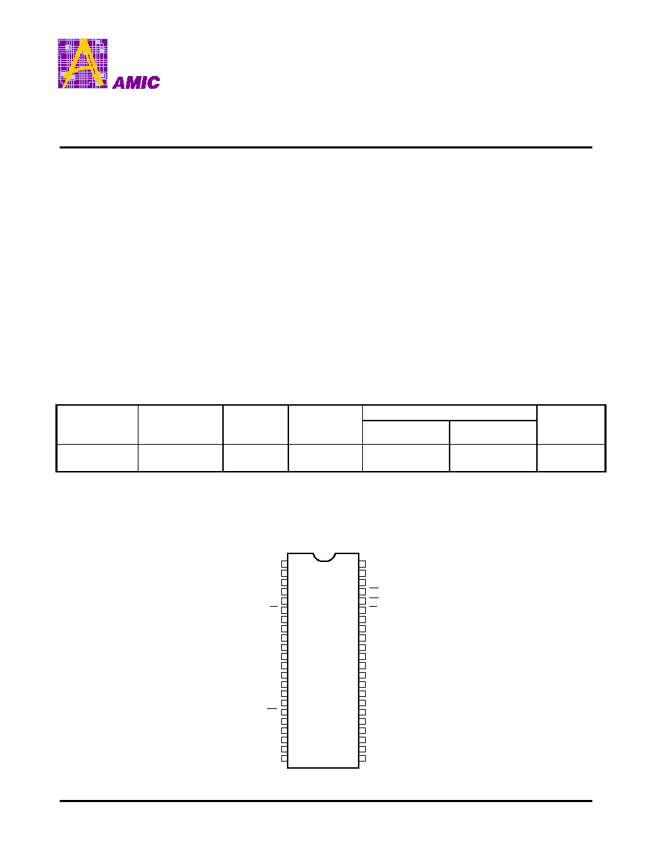
Pin Configuration
n
SOJ / TSOP (II)
1
A0
A1
A2
A3
A4
CE
I/O
0
I/O
1
I/O
2
I/O
3
VCC
GND
I/O
4
I/O
5
I/O
6
I/O
7
23
30
31
32
33
34
35
36
37
38
39
40
41
42
43
44
2
3
4
5
6
7
8
9
10
11
12
13
14
15
16
A15
A14
A13
OE
HB
LB
I/O
15
I/O
14
I/O
13
I/O
12
VCC
GND
I/O
11
I/O
10
I/O
9
I/O
8
A61L6316S(V)
17
18
19
20
21
22
24
25
26
27
28
29
WE
A5
A6
A7
A8
NC
NC
A12
A11
A10
A9
NC
A61L6316 Series
(July, 2002, Version 1.1)
2
AMIC Technology, Inc.
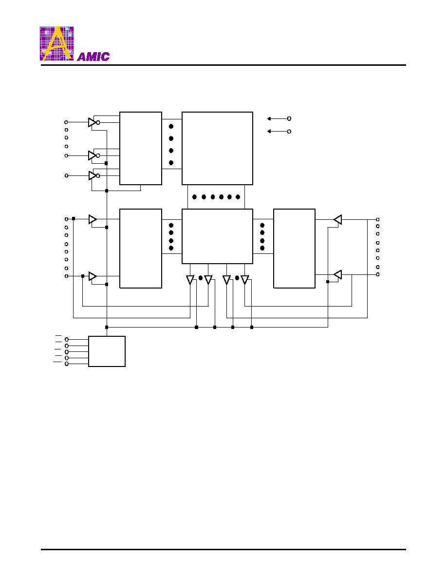
Block Diagram
DECODER
1,048,576-BIT
MEMORY ARRAY
COLUMN I/O
INPUT
DATA
CIRCUIT
CONTROL
CIRCUIT
VCC
GND
I/O
7
I/O
0
A15
A14
A0
WE
HB
INPUT
DATA
CIRCUIT
I/O
8
I/O
15
CE
LB
OE
A61L6316 Series
(July, 2002, Version 1.1)
3
AMIC Technology, Inc.
Pin Description - SOJ/TSOP(II)
Pin No.
Symbol
Description
1 - 5, 18 - 21,
24 - 27,42 - 44
A0 - A15
Address Inputs
6
CE
Chip Enable Input
7 - 10, 13 - 16,
29 - 32, 35 - 38
I/O
0
- I/O
15
Data Input/Outputs
17
WE
Write Enable Input
39
LB
Byte Enable Input (I/O
0
to I/O
7
)
40
HB
Byte Enable Input (I/O
8
to I/O
15
)
41
OE
Output Enable Input
11, 33
VCC
Power
12, 34
GND
Ground
22 , 23, 28
NC
No Connection
Recommended DC Operating Conditions
(T
A
= 0
�
C to + 70
�
C or -25
�
C to +85
�
C)
Symbol
Parameter
Min.
Typ.
Max.
Unit
*VCC
Supply Voltage
3.0
3.3
3.6
V
GND
Ground
0
0
0
V
V
IH
Input High Voltage
2.2
-
VCC + 0.3
V
V
IL
Input Low Voltage
-0.3
-
0.8
V
C
L
Output Load
-
-
30
pF
* -10 V
CC
min
: 3.135V
A61L6316 Series
(July, 2002, Version 1.1)
4
AMIC Technology, Inc.
Absolute Maximum Ratings*
VCC to GND . . . . . . . . . . . . . . . . . . . . . . -0.5V to +4.6V
IN, IN/OUT Volt to GND . . . . . . . . -0.5V to VCC + 0.5V
Operating Temperature, Topr . . . . . . . . . . . . . . . . . . . . .
. . . . . . . . . . . . . . . . . . . 0
�
C to +70
�
C or -25
�
C to +85
�
C
Storage Temperature, Tstg . . . . . . . . . -55
�
C to +125
�
C
Power Dissipation, P
T
. . . . . . . . . . . . . . . . . . . . . 0.7W
Soldering Temp. & Time . . . . . . . . . . . . . 260
�
C, 10 sec
*Comments
Stresses above those listed under "Absolute Maximum
Ratings" may cause permanent damage to this device.
These are stress ratings only. Functional operation of this
device at these or any other conditions above those
indicated in the operational sections of this specification
is not implied or intended. Exposure to the absolute
maximum rating conditions for extended periods may
affect device reliability.
DC Electrical Characteristics
(T
A
= 0
�
C to + 70
�
C or -25
�
C to +85
�
C, -10: 3.3V+10%, -5%; -12, -15: 3.3V�10%)
Symbol
Parameter
A61L6316-10 A61L6316-12
A61L6316-15
Unit
Conditions
Min.
Max.
Min.
Max.
Min.
Max.
I
LI
Input Leakage
-
2
-
2
-
2
�
A
V
IN
= GND to VCC
I
LO
Output Leakage
-
2
-
2
-
2
�
A
CE = V
IH
, OE = V
IH
V
I/O
= GND to VCC
I
CC1
(2)
Dynamic Operating
Current
-
230
-
220
-
210
mA
CE = V
IL
, I
I/O
= 0 mA
Min. Cycle, Duty = 100%
I
SB
-
25
-
25
-
25
mA
CE = V
IH
I
SB1
Standby Power
Supply Current
-
12
-
12
-
12
mA
CE
VCC - 0.2V,
V
IN
VCC -0.2V or
V
IN
0.2V
V
OL
Output Low Voltage
-
0.4
-
0.4
-
0.4
V
I
OL
= 8 mA
V
OH
Output High Voltage
2.4
-
2.4
-
2.4
-
V
I
OH
= -4 mA
Notes: 1. V
IL
= -3.0V for pulses less than 20 ns.
2. I
CC1
is dependent on output loading, cycle rates, and Read/Write patterns.