
A61L6316 Series
64K X 16 BIT HIGH SPEED CMOS SRAM
(July, 2002, Version 1.1)
AMIC Technology, Inc.
Document Title
64K X 16 BIT HIGH SPEED CMOS SRAM
Revision History
Rev. No. History
Issue Date
Remark
0.0
Initial issue
July 14, 2000
Preliminary
1.0
Final spec. release
May 8, 2001
Final
Add -10 spec.
Change I
CC1
from 120mA to 220mA (-12)
Change I
CC1
from 100mA to 210mA (-15)
Change I
SB1
from 8mA to 12mA
Change I
CDR
from 1mA to 5mA
Add t
BE
, t
BLZ
, t
BHZ
, t
BW
parameters
1.1
Add -25
∞
C ~ +85
∞
C grade
July 17, 2002

A61L6316 Series
64K X 16 BIT HIGH SPEED CMOS SRAM
(July, 2002, Version 1.1)
1
AMIC Technology, Inc.
Features
General Description
n
Center power pinout
n
Supply voltage: -10: 3.3V+10%, -5%
-12, -15: 3.3V±10%
n
Access times: 10/12/15 ns (max.)
n
Current: Operating: -10: 230mA (max)
-12: 220mA (max.)
-15: 210mA (max.)
Standby: TTL: 25mA (max.)
CMOS: 12mA (max.)
n
Extended operating temperature range: -25
∞
C to 85
∞
C
for -I series
n
Full static operation, no clock or refreshing required
n
All inputs and outputs are directly TTL-compatible
n
Common I/O using three-state output
n
Data retention voltage: 2V (min.)
n
Available in 44-pin 400mil SOJ and 44-pin 400mil
TSOP(II) forward packages.
The A61L6316 is a high speed 1,048,576-bit static
random access memory organized as 65,536 words by 16
bits and operates on low power supply voltage from 3.0V
to 3.6V. It is built using AMIC's high performance CMOS
process.
Inputs and three-state outputs are TTL compatible and
allow for direct interfacing with common system bus
structures.
The chip enable input is provided for POWER-DOWN, to
disable the device. Two byte enable inputs and an output
enable input are included for easy interfacing.
Data retention is guaranteed at a power supply voltage as
low as 2V.
Product Family
Power Dissipation
Product
Family
Operating
Temperature
VCC Range
Speed
Data Retention
(I
CCDR
, Typ.)
Standby
(I
SB1
, Typ.)
Package
Type
A61L6316
0
∞
C ~ +70
∞
C
-25
∞
C ~ +85
∞
C
3.0V ~ 3.6V
10/12/15 ns
3mA
5mA
44L SOP
44L TSOP(II)
1. Typical values are measured at VCC = 3.3V, T
A
= 25
∞
C and not 100% tested.
2. Data retention current VCC = 2.0V.
Pin Configuration
n
SOJ / TSOP (II)
1
A0
A1
A2
A3
A4
CE
I/O
0
I/O
1
I/O
2
I/O
3
VCC
GND
I/O
4
I/O
5
I/O
6
I/O
7
23
30
31
32
33
34
35
36
37
38
39
40
41
42
43
44
2
3
4
5
6
7
8
9
10
11
12
13
14
15
16
A15
A14
A13
OE
HB
LB
I/O
15
I/O
14
I/O
13
I/O
12
VCC
GND
I/O
11
I/O
10
I/O
9
I/O
8
A61L6316S(V)
17
18
19
20
21
22
24
25
26
27
28
29
WE
A5
A6
A7
A8
NC
NC
A12
A11
A10
A9
NC

A61L6316 Series
(July, 2002, Version 1.1)
2
AMIC Technology, Inc.
Block Diagram
DECODER
1,048,576-BIT
MEMORY ARRAY
COLUMN I/O
INPUT
DATA
CIRCUIT
CONTROL
CIRCUIT
VCC
GND
I/O
7
I/O
0
A15
A14
A0
WE
HB
INPUT
DATA
CIRCUIT
I/O
8
I/O
15
CE
LB
OE

A61L6316 Series
(July, 2002, Version 1.1)
3
AMIC Technology, Inc.
Pin Description - SOJ/TSOP(II)
Pin No.
Symbol
Description
1 - 5, 18 - 21,
24 - 27,42 - 44
A0 - A15
Address Inputs
6
CE
Chip Enable Input
7 - 10, 13 - 16,
29 - 32, 35 - 38
I/O
0
- I/O
15
Data Input/Outputs
17
WE
Write Enable Input
39
LB
Byte Enable Input (I/O
0
to I/O
7
)
40
HB
Byte Enable Input (I/O
8
to I/O
15
)
41
OE
Output Enable Input
11, 33
VCC
Power
12, 34
GND
Ground
22 , 23, 28
NC
No Connection
Recommended DC Operating Conditions
(T
A
= 0
∞
C to + 70
∞
C or -25
∞
C to +85
∞
C)
Symbol
Parameter
Min.
Typ.
Max.
Unit
*VCC
Supply Voltage
3.0
3.3
3.6
V
GND
Ground
0
0
0
V
V
IH
Input High Voltage
2.2
-
VCC + 0.3
V
V
IL
Input Low Voltage
-0.3
-
0.8
V
C
L
Output Load
-
-
30
pF
* -10 V
CC
min
: 3.135V

A61L6316 Series
(July, 2002, Version 1.1)
4
AMIC Technology, Inc.
Absolute Maximum Ratings*
VCC to GND . . . . . . . . . . . . . . . . . . . . . . -0.5V to +4.6V
IN, IN/OUT Volt to GND . . . . . . . . -0.5V to VCC + 0.5V
Operating Temperature, Topr . . . . . . . . . . . . . . . . . . . . .
. . . . . . . . . . . . . . . . . . . 0
∞
C to +70
∞
C or -25
∞
C to +85
∞
C
Storage Temperature, Tstg . . . . . . . . . -55
∞
C to +125
∞
C
Power Dissipation, P
T
. . . . . . . . . . . . . . . . . . . . . 0.7W
Soldering Temp. & Time . . . . . . . . . . . . . 260
∞
C, 10 sec
*Comments
Stresses above those listed under "Absolute Maximum
Ratings" may cause permanent damage to this device.
These are stress ratings only. Functional operation of this
device at these or any other conditions above those
indicated in the operational sections of this specification
is not implied or intended. Exposure to the absolute
maximum rating conditions for extended periods may
affect device reliability.
DC Electrical Characteristics
(T
A
= 0
∞
C to + 70
∞
C or -25
∞
C to +85
∞
C, -10: 3.3V+10%, -5%; -12, -15: 3.3V±10%)
Symbol
Parameter
A61L6316-10 A61L6316-12
A61L6316-15
Unit
Conditions
Min.
Max.
Min.
Max.
Min.
Max.
I
LI
Input Leakage
-
2
-
2
-
2
µ
A
V
IN
= GND to VCC
I
LO
Output Leakage
-
2
-
2
-
2
µ
A
CE = V
IH
, OE = V
IH
V
I/O
= GND to VCC
I
CC1
(2)
Dynamic Operating
Current
-
230
-
220
-
210
mA
CE = V
IL
, I
I/O
= 0 mA
Min. Cycle, Duty = 100%
I
SB
-
25
-
25
-
25
mA
CE = V
IH
I
SB1
Standby Power
Supply Current
-
12
-
12
-
12
mA
CE
VCC - 0.2V,
V
IN
VCC -0.2V or
V
IN
0.2V
V
OL
Output Low Voltage
-
0.4
-
0.4
-
0.4
V
I
OL
= 8 mA
V
OH
Output High Voltage
2.4
-
2.4
-
2.4
-
V
I
OH
= -4 mA
Notes: 1. V
IL
= -3.0V for pulses less than 20 ns.
2. I
CC1
is dependent on output loading, cycle rates, and Read/Write patterns.

A61L6316 Series
(July, 2002, Version 1.1)
5
AMIC Technology, Inc.
Truth Table
CE
OE
WE
LB
HB
I/O
0
to I/O
7
Mode
I/O
8
to I/O
15
Mode
VCC Current
H
X
X
X
X
Not selected
Not selected
I
SB1
, I
SB
L
L
Read
Read
I
CC1
, I
CC2
, I
CC
L
L
H
L
H
Read
High - Z
I
CC1
, I
CC2
, I
CC
H
L
High - Z
Read
I
CC1
, I
CC2
, I
CC
L
L
Write
Write
I
CC1
, I
CC2
, I
CC
L
X
L
L
H
Write
Not Write/Hi - Z
I
CC1
, I
CC2
, I
CC
H
L
Not Write/Hi - Z
Write
I
CC1
, I
CC2
, I
CC
L
X
High - Z
High - Z
I
CC1
, I
CC2
, I
CC
L
H
H
X
L
High - Z
High - Z
I
CC1
, I
CC2
, I
CC
X
X
X
H
H
Not selected
Not selected
I
SB1
, I
SB
Note: X = H or L
Capacitance
(T
A
= 25
∞
C, f = 1.0MHz)
Symbol
Parameter
Min.
Max.
Unit
Conditions
C
IN
*
Input Capacitance
-
6
pF
V
IN
= 0V
C
I/O
*
Input/Output Capacitance
-
8
pF
V
I/O
= 0V
* These parameters are sampled and not 100% tested.

A61L6316 Series
(July, 2002, Version 1.1)
6
AMIC Technology, Inc.
AC Characteristics
(T
A
= 0
∞
C to +70
∞
C or -25
∞
C to +85
∞
C, -10: 3.3V+10%, -5%; -12, -15: 3.3V±10%)
Symbol
Parameter
A61L6316-10
A61L6316-12
A61L6316-15
Unit
Min.
Max.
Min.
Max.
Min.
Max.
Read Cycle
t
RC
Read Cycle Time
10
-
12
-
15
-
ns
t
AA
Address Access Time
-
10
-
12
-
15
ns
t
ACE
Chip Enable Access Time
-
10
-
12
-
15
ns
t
BE
Byte Enable Access Time
-
5
-
6
-
8
ns
t
OE
Output Enable to Output Valid
-
5
-
6
-
8
ns
t
CLZ
Chip Enable to Output in Low Z
3
-
3
-
3
-
ns
t
OLZ
Output Enable to Output in Low Z
0
-
0
-
0
-
ns
t
BLZ
Byte Enable to Output in Low Z
0
-
0
-
0
-
ns
t
CHZ
Chip Disable Output in High Z
0
5
0
6
-
8
ns
t
BHZ
Byte Disable to Output in High Z
0
5
0
6
0
8
ns
t
OHZ
Output Disable to Output in High Z
0
5
0
6
0
8
ns
t
OH
Output Hold from Address Change
3
-
3
-
3
-
ns
Write Cycle
t
WC
Write Cycle Time
10
-
12
-
15
-
ns
t
CW
Chip Enable to End of Write
8
-
10
-
12
-
ns
t
BW
Byte Enable to End of Write
8
-
10
-
12
-
ns
t
AS
Address Setup Time of Write
0
-
0
-
0
-
ns
t
AW
Address Valid to End of Write
8
-
10
-
12
-
ns
t
WP
Write Pulse Width
8
-
10
-
12
-
ns
t
WR
Write Recovery Time
0
-
0
-
0
-
ns
t
WHZ
Write to Output in High Z
0
5
0
6
0
8
ns
t
DW
Data to Write Time Overlap
5
-
6
-
7
-
ns
t
DH
Data Hold from Write Time
0
-
0
-
0
-
ns
t
OW
Output Active from End of Write
3
-
3
-
3
-
ns
Notes: t
CHZ
, t
BHZ
, t
OHZ
and t
WHZ
are defined as the time at which the outputs achieve the open circuit condition and are not
referred to output voltage levels.

A61L6316 Series
(July, 2002, Version 1.1)
7
AMIC Technology, Inc.
Timing Waveforms
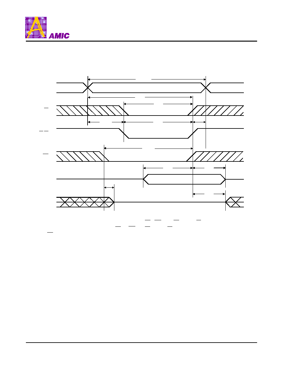
Read Cycle 1
(1, 2, 4)
t
RC
t
OH
t
AA
t
OH
Address
D
OUT
Read Cycle 2
(1, 2, 3)
t
RC
t
AA
Address
t
ACE
t
CHZ5
CE
HB, LB
t
BHZ5
OE
t
CLZ5
t
BE
t
BLZ5
t
OE
t
OLZ5
t
OHZ5
D
OUT
Notes: 1. WE is high for Read Cycle.
2. Device is continuously enabled CE = V
IL
, HB = V
IL
and, or LB = V
IL
.
3. Address valid prior to or coincident with CE and ( HB and, or LB ) transition low.
4. OE = V
IL
.
5. Transition is measured
±
200mV from steady state. This parameter is sampled and not 100% tested.

A61L6316 Series
(July, 2002, Version 1.1)
8
AMIC Technology, Inc.
Timing Waveforms (continued)
Write Cycle 1
(Write Enable Controlled)
t
WC
t
AW
Address
DATA IN
DATA OUT
WE
HB, LB
CE
t
WR3
t
CW
t
BW
t
AS1
t
WP2
t
DW
t
DH
t
OW
t
WHZ4

A61L6316 Series
(July, 2002, Version 1.1)
9
AMIC Technology, Inc.
Timing Waveforms (continued)
Write Cycle 2
(Chip Enable Controlled)
t
WC
t
AW
Address
DATA IN
DATA OUT
WE
HB, LB
CE
t
WR3
t
CW2
t
BW
t
AS1
t
WP
t
DW
t
DH
t
OW
t
WHZ4
A61L6316 Series
(July, 2002, Version 1.1)
10
AMIC Technology, Inc.
Timing Waveforms (continued)
Write Cycle 3
(Byte Enable Controlled)
t
WC
t
AW
Address
DATA IN
DATA OUT
WE
HB, LB
CE
t
WR3
t
CW
t
BW2
t
AS1
t
WP
t
DW
t
DH
t
OW
t
WHZ4
Notes: 1. t
AS
is measured from the address valid to the beginning of Write.
2. A Write occurs during the overlap (t
WP
, t
BW
) of a low CE , WE and ( HB and, or LB ).
3. t
WR
is measured from the earliest of CE or WE or ( HB and, or LB ) going high to the end of the Write cycle.
4. OE level is high or low.
5. Transition is measured
±
200mV from steady state. This parameter is sampled and not 100% tested.
A61L6316 Series
(July, 2002, Version 1.1)
11
AMIC Technology, Inc.
AC Test Conditions
Input Pulse Levels
0V to 3.0V
Input Rise And Fall Time
3 ns
Input and Output Timing Reference Levels
1.5 V
Output Load
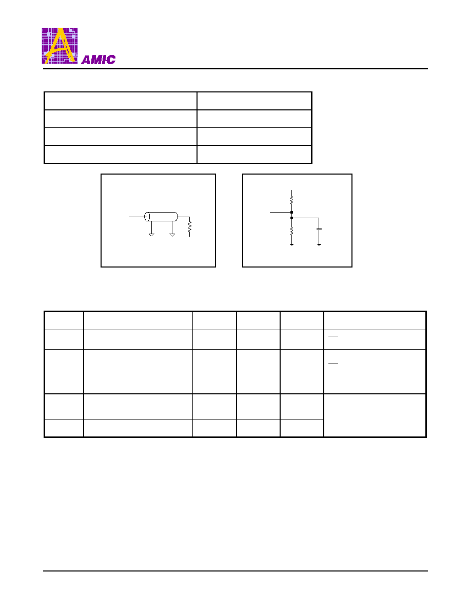
See Figures 1 and 2
+3.3V
I/O
351
317
5pF*
* Including scope and jig.
Z
O
=50
OUTPUT
R
L
=50
V
T
=1.5V
Figure 1. Output Load
Figure 2. Output Load for t
CLZ
,
t
OLZ
,
t
CHZ
,
t
OHZ
,
t
WHZ
,
and t
OW
Data Retention Characteristics
(T
A
= 0
∞
C to 70
∞
C or -25
∞
C to +85
∞
C)
Symbol
Parameter
Min.
Max.
Unit
Conditions
V
DR
VCC for Data Retention
2
3.6
V
CE
VCC - 0.2V
I
CCDR
Data Retention Current
-
5
mA
VCC = 2.0V
CE
VCC - 0.2V
V
IN
VCC - 0.2V or
V
IN
0.2V
t
CDR
Chip Disable to Data Retention
Time
0
-
ns
See Retention Waveform
t
R
Operation Recovery Time
T
RC
*
-
ms
t
RC
= Read Cycle Time

A61L6316 Series
(July, 2002, Version 1.1)
12
AMIC Technology, Inc.
Low VCC Data Retention Waveform
VCC
CE
t
CDR
V
IH
3.0V
t
R
V
IH
3.0V
DATA RETENTION MODE
V
DR
2V
CE
V
DR
- 0.2V
t
VR
Ordering Information
Part No.
Access Time (ns)
Operating Current
Max. (mA)
Standby Current
Max. (mA)
Package
A61L6316S-10
44L SOJ
A61L6316S-10I
44L SOJ
A61L6316V-10
44L TSOP(II)
A61L6316V-10I
10
230
12
44L TSOP(II)
A61L6316S-12
44L SOJ
A61L6316S-12I
44L SOJ
A61L6316V-12
44L TSOP(II)
A61L6316V-12I
12
220
12
44L TSOP(II)
A61L6316S-15
44L SOJ
A61L6316S-15I
44L SOJ
A61L6316V-15
44L TSOP(II)
A61L6316V-15I
15
210
12
44L TSOP(II)
* I series for -25
∞
C to +85
∞
C

A61L6316 Series
(July, 2002, Version 1.1)
13
AMIC Technology, Inc.
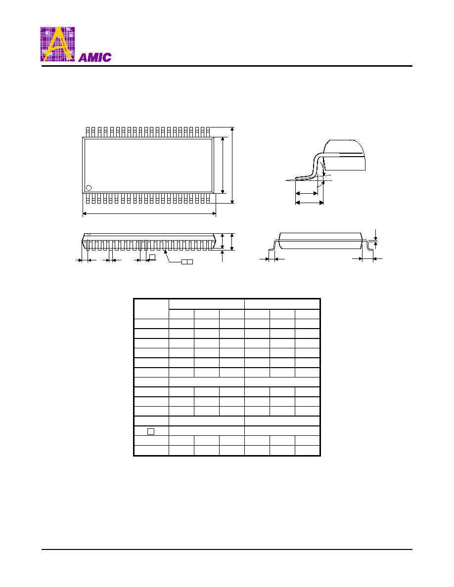
Package Information
SOJ 44L Outline Dimensions
unit: inches/mm
Dimensions in inches
Dimensions in mm
Symbol
Min
Nom
Max
Min
Nom
Max
A
0.128
0.138
0.148
3.25
3.51
3.76
A
1
0.082
-
-
2.08
-
-
A
2
0.105
0.110
0.115
2.67
2.79
2.92
b
0.015
-
0.020
0.38
-
0.51
b
1
0.026
0.028
0.032
0.66
0.71
0.81
C
0.007
-
0.013
0.18
-
0.21
D
1.120
1.125
1.130
28.45
28.58
28.70
E
0.435
0.440
0.445
11.05
11.18
11.30
E
1
0.394
0.400
0.405
10.01
10.16
10.29
E
2
0.370 BSC
9.40 BSC
e
0.050 BSC
1.27 BSC
R
1
0.030
0.035
0.040
0.76
0.89
1.02
0
∞
-
10
∞
0
∞
-
10
∞
Notes:
1. The maximum value of dimension D includes end flash.
2. Dimension E does not include resin fins.
3. Dimension E
1
is for PC Board surface mount pad pitch design
reference only.
b
b
1
D
y
0.004
A
2
A
A
1
y
e
R
1
C
E
2
E
E
1
Seating Plane
D
44
23
22
1
Min
0.025"
A61L6316 Series
(July, 2002, Version 1.1)
14
AMIC Technology, Inc.
Package Information
TSOP 44L (Type II) Outline Dimensions
unit: inches/mm
1
E
L
1
L
1
c
44
ZD
D y
e
D
b
L
L
A
1
A
2
A
E
1
Dimensions in inches
Dimensions in mm
Symbol
Min
Nom
Max
Min
Nom
Max
A
-
-
0.047
-
-
1.20
A
1
0.002
-
0.006
0.05
-
0.15
A
2
0.037
0.039
0.041
0.95
1.00
1.05
b
0.012
-
0.018
0.30
-
0.45
c
0.005
-
0.008
0.12
-
0.21
D
0.720
0.725
0.730
18.28
18.41
18.54
ZD
0.032 REF
0.805 REF
E
0.455
0.463
0.471
11.56
11.76
11.96
E
1
0.395
0.400
0.405
10.03
10.16
10.29
L
0.019
0.023
0.027
0.49
0.59
0.69
L
1
0.031 REF
0.80 REF
e
0.031 BSC
0.80 BSC
y
-
-
0.004
-
-
0.10
0∞
-
5∞
0∞
-
5∞
Notes:
1. The maximum value of dimension D includes end flash.
2. Dimension E
1
does not include resin fins.
3. Dimension ZD includes end flash.