 | ÐлекÑÑоннÑй компоненÑ: A625308AV | СкаÑаÑÑ:  PDF PDF  ZIP ZIP |
þÿ
A625308A Series
Preliminary
32K X 8 BIT CMOS SRAM
PRELIMINARY (November, 2001, Version 0.1)
AMIC Technology, Inc.
Document Title
32K X 8 BIT CMOS SRAM
Revision History
Rev. No. History
Issue Date
Remark
0.0
Initial issue
February 2, 2001
Preliminary
0.1
Add ultra temp grade and 28-pin DIP package type
November 7, 2001
A625308A Series
Preliminary
32K X 8 BIT CMOS SRAM
PRELIMINARY (November, 2001, Version 0.1)
1
AMIC Technology, Inc.
Features
n
Power Supply Range: 4.5V to 5.5V
n
Access times: 70 ns
A625308A-S series:
Operating: 35mA (max.)
Standby: 10
µ
A (max.)
A625308A-SU series:
Operating: 35mA (max.)
Standby: 15
µ
A (max.)
n
Extended operating temperature range: -40
°
C to 85
°
C
for -SU series.
n
Full static operation, no clock or refreshing required
n
All inputs and outputs are directly TTL-compatible
n
Common I/O using three-state output
n
Data retention voltage: 2.0V (min.)
n
Available in 28-pin, DIP/SOP and TSOP
General Description
The A625308A is a low operating current 262,144-bit
static random access memory organized as 32,768
words by 8 bits and operates on a voltage from 4.5V to
5.5V.
Inputs and three-state outputs are TTL compatible and
allow for direct interfacing with common system bus
structures.
Minimum standby power is drawn by this device when
CE is at a high level, independent of the other input
levels.
Data retention is guaranteed at a power supply voltage
as low as 2.0V.
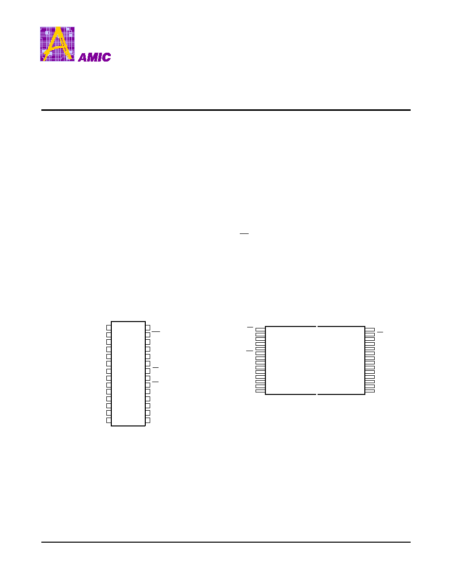
Pin Configurations
n
DIP / SOP
n
TSOP
A14
A12
A7
A6
A5
A4
A3
A2
A1
A0
I/O
0
I/O
1
I/O
2
GND
I/O
3
I/O
4
I/O
5
I/O
6
I/O
7
CE
OE
A11
A9
A8
A13
WE
VCC
A10
A625308A(M)
1
2
3
4
5
6
7
8
9
10
11
12
13
14
15
16
17
18
19
20
21
22
23
24
25
26
27
28
A625308AV
1
9
28
20
A11
2
3
4
5
6
7
8
10
11
12
13
14
A9
A8
A13
A14
A12
A7
A6
A5
A4
A3
27
26
25
24
23
22
21
19
18
17
16
15
I/O
6
I/O
5
I/O
4
I/O
3
VSS
I/O
2
I/O
1
I/O
0
A0
A1
A2
A10
VCC
I/O
7
OE
WE
CE
~ ~
~ ~
A625308A Series
PRELIMINARY (November, 2001, Version 0.1)
2
AMIC Technology, Inc.
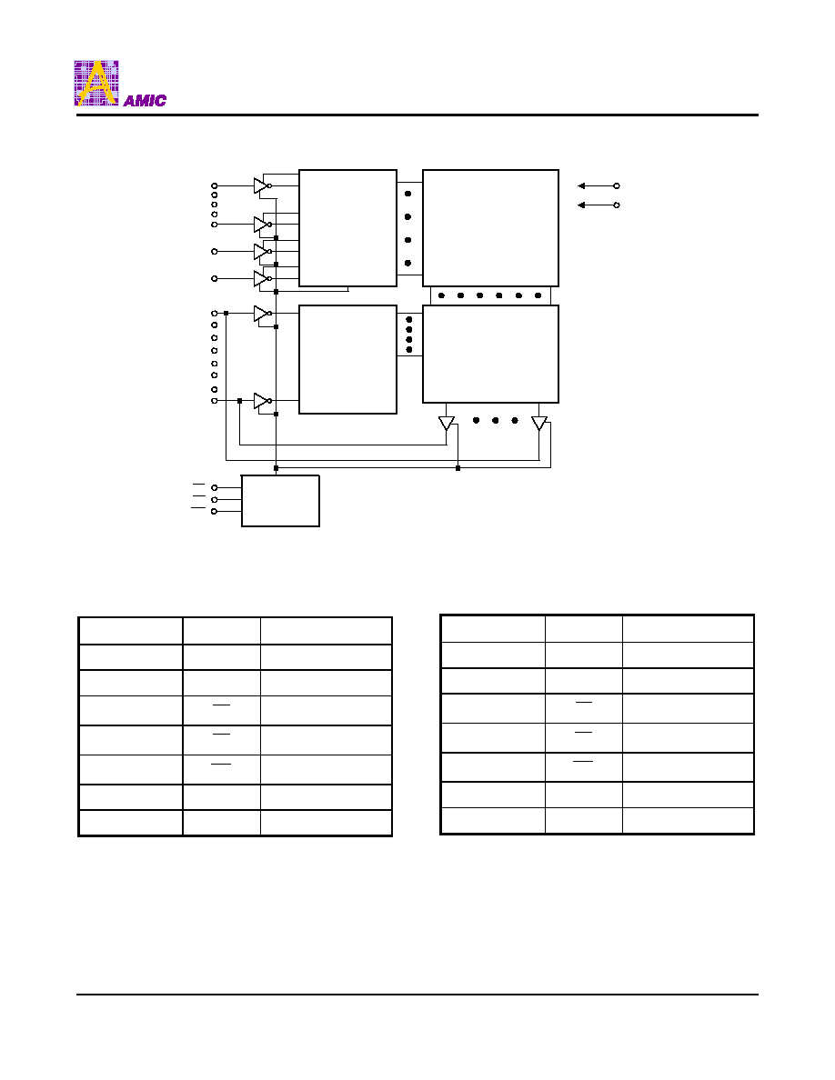
Block Diagram
ROW
DECODER
512 X 512
MEMORY ARRAY
INPUT DATA
CIRCUIT
COLUMN I/O
CONTROL
CIRCUIT
CE
WE
I/O
7
I/O
0
A14
A13
A12
A0
VCC
GND
OE
Pin Descriptions DIP / SOP
Pin No.
Symbol
Description
1-10, 21, 23-26
A0 - A14
Address Input
11-13, 15-19
I/O
0
- I/O
7
Data Input/Output
20
CE
Chip Enable
22
OE
Output Enable
27
WE
Write Enable
28
VCC
Power Supply
14
GND
Ground
Pin Description-TSOP
Pin No.
Symbol
Description
2-5, 8-17, 28
A0 - A14
Address Input
18-20, 22-26
I/O
0
- I/O
7
Data Input/Output
27
CE
Chip Enable
1
OE
Output Enable
6
WE
Write Enable
7
VCC
Power Supply
21
GND
Ground
A625308A Series
PRELIMINARY (November, 2001, Version 0.1)
3
AMIC Technology, Inc.
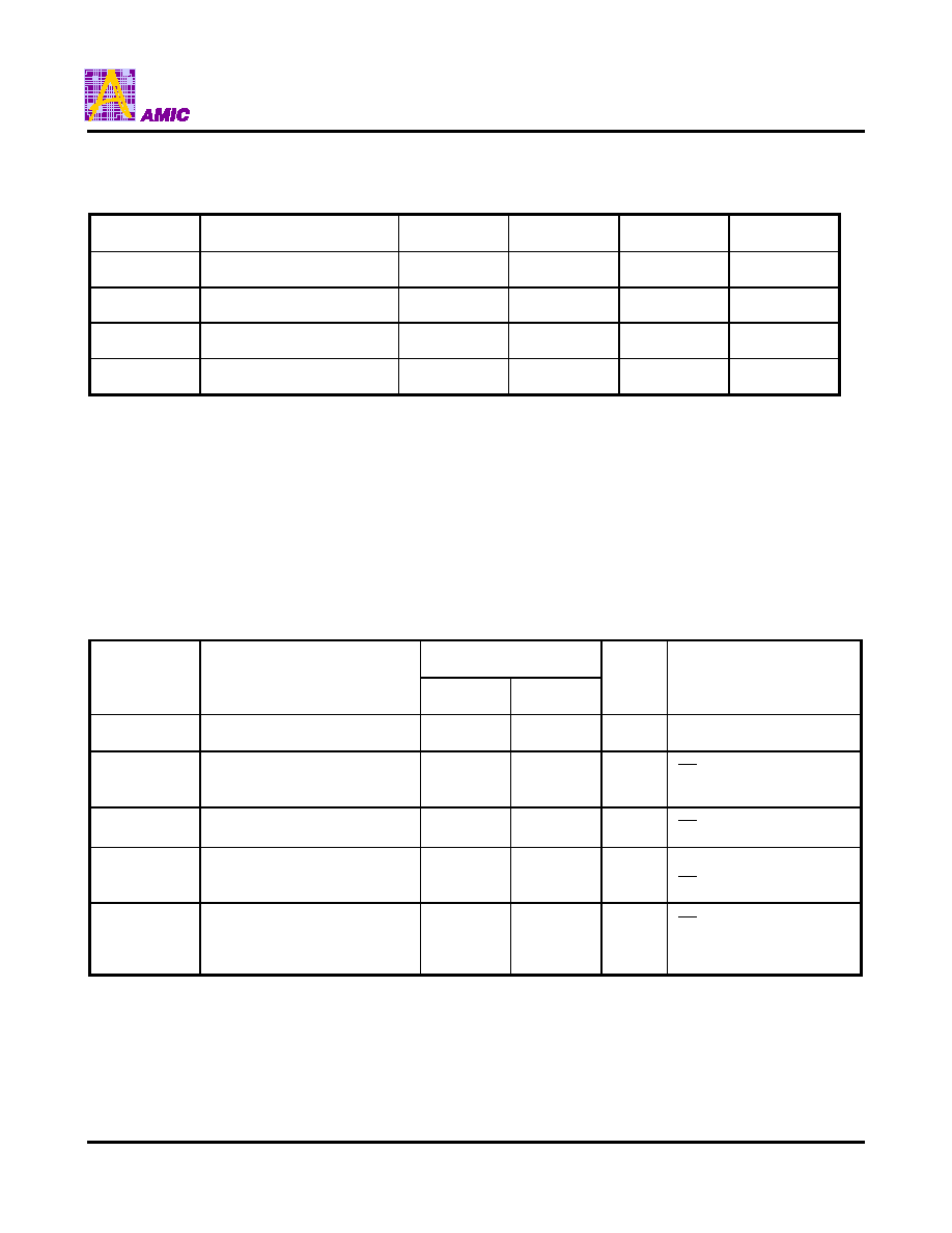
Recommended DC Operating Conditions
(T
A
= 0
°
C to +70
°
C or -40
°
C to +85
°
C)
Symbol
Parameter
Min.
Typ.
Max.
Unit
VCC
Supply Voltage
4.5
5.0
5.5
V
GND
Ground
0
0
0
V
V
IH
Input High Voltage
2.2
-
VCC + 0.5
V
V
IL
Input Low Voltage
-0.5
0
+0.8
V
Absolute Maximum Ratings*
VCC to GND . . . . . . . . . . . . . . . . . . . . . . -0.5V to +7.0V
IN, IN/OUT Volt to GND . . . . . . . . . -0.5V to VCC + 0.5V
Operating Temperature, Topr . . . . . . . . . . . . . . . . . . . . . .
. . . . . . . . . . . . . . . . . . . . 0
°
C to +70
°
C or -40
°
C to +85
°
C
Storage Temperature, Tstg . . . . . . . . . -55
°
C to +125
°
C
Power Dissipation, P
T
. . . . . . . . . . . . . . . . . . . . . . 0.7W
Soldering Temp. & Time . . . . . . . . . . . . . 260
°
C, 10 sec
*Comments
Stresses above those listed under "Absolute Maximum
Ratings" may cause permanent damage to the device.
These are stress ratings only. Functional operation of this
device at these or any other conditions above those
indicated in the operational sections of this specification
is not implied and exposure to absolute maximum rating
conditions for extended periods may affect device
reliability.
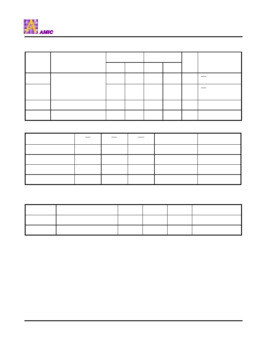
DC Electrical Characteristics
(T
A
= 0
°
C to +70
°
C or -40
°
C to +85
°
C, VCC = 5.0V
±
10%, GND = 0V)
Symbol
Parameter
A625308A-70S/SU
Unit
Conditions
Min.
Max.
I
LI
Input Leakage Current
-
1
µ
A
V
IN
= GND to VCC
I
LO
Output Leakage Current
-
1
µ
A
CE = V
IH
V
I/O
= GND to VCC
I
CC
Active Power Supply Current
-
5
mA
CE = V
IL
, I
I/O
= 0mA
I
CC1
Dynamic Operating Current
-
35
mA
Min. Cycle, Duty = 100%
CE = V
IL
, I
I/O
= 0mA
I
CC2
Dynamic Operating Current
-
5
mA
CE = V
IL
, V
IH
= VCC
V
IL
= 0V, f = 1 MHz
I
I/O
= 0 mA
A625308A Series
PRELIMINARY (November, 2001, Version 0.1)
4
AMIC Technology, Inc.
DC Electrical Characteristics (continued)
Symbol
Parameter
A625308A-70S
A625308A-70SU
Unit
Conditions
Min.
Max.
Min.
Max.
I
SB
Supply Current
-
0.5
-
0.5
mA
CE = V
IH
I
SB1
Standby Power
-
10
-
15
µ
A
CE
VCC - 0.2V
V
IN
0V
V
OL
Output Low Voltage
-
0.4
-
0.4
V
I
OL
= 2.1 mA
V
OH
Output High Voltage
2.4
-
2.4
-
V
I
OH
= -1.0 mA
Truth Table
Mode
CE
OE
WE
I/O Operation
Supply Current
Standby
H
X
X
High Z
I
SB
, I
SB1
Output Disable
L
H
H
High Z
I
CC
, I
CC1
, I
CC2
Read
L
L
H
D
OUT
I
CC
, I
CC1
, I
CC2
Write
L
X
L
D
IN
I
CC
, I
CC1
, I
CC2
Note: X: H or L
Capacitance
(T
A
= 25
°
C, f = 1.0 MHz)
Symbol
Parameter
Min.
Max.
Unit
Conditions
C
IN
*
Input Capacitance
-
6
pF
V
IN
= 0V
C
I/O
*
Input/Output Capacitance
-
8
pF
V
I/O
= 0V
* These parameters are sampled and not 100% tested.