Äîêóìåíòàöèÿ è îïèñàíèÿ www.docs.chipfind.ru

A63L83361
256K X 36 Bit Synchronous High Speed SRAM with
Preliminary
Burst Counter and Flow-through Data Output
PRELIMINARY (July, 2005, Version 0.0)
AMIC Technology, Corp.
Document Title
256K X 36 Bit Synchronous High Speed SRAM with Burst Counter and Flow-
through Data Output
Revision History
Rev. No. History Issue
Date Remark
0.0
Initial issue
July 14, 2005
Preliminary

A63L83361
256K X 36 Bit Synchronous High Speed SRAM with
Preliminary
Burst Counter and Flow-through Data Output
PRELIMINARY (July, 2005, Version 0.0)
1
AMIC Technology, Corp.
Features
Fast access times: 6.5/7.5/8.0 ns(153/133/117 MHz)
Single 3.3V
±
5% power supply
Synchronous burst function
Individual Byte Write control and Global Write
Three separate chip enables allow wide range of
options for CE control, address pipelining
Selectable BURST mode
SLEEP mode (ZZ pin) provided
Available in 100-pin LQFP package
Industrial operating temperature range: -45
°
C to
+125
°
C for -I series
General Description
The A63L83361 is a high-speed SRAM containing 9M bits
of bit synchronous memory, organized as 256K words by
36 bits.
The A63L83361 combines advanced synchronous
peripheral circuitry, 2-bit burst control, input registers,
output buffer and a 256K X 36 SRAM core to provide a
wide range of data RAM applications.
The positive edge triggered single clock input (CLK)
controls all synchronous inputs passing through the
registers. Synchronous inputs include all addresses (A0 -
A17), all data inputs (I/O
1
- I/O
36
), active LOW chip
enable (
CE ), two additional chip enables (CE2, CE2 ),
burst control inputs ( ADSC , ADSP , ADV ), byte write
enables ( BWE , BW1 , BW2 , BW3 , BW4 ) and Global
Write ( GW ). Asynchronous inputs include output enable
( OE ), clock (CLK), BURST mode (MODE) and SLEEP
mode (ZZ).
Burst operations can be initiated with either the address
status processor ( ADSP ) or address status controller
( ADSC ) input pin. Subsequent burst sequence burst
addresses can be internally generated by the A63L83361
and controlled by the burst advance ( ADV ) pin. Write
cycles are internally self-timed and synchronous with the
rising edge of the clock (CLK).
This feature simplifies the write interface. Individual Byte
enables allow individual bytes to be written. BW1 controls
I/O
1
- I/O
9
, BW2 controls I/O
10
- I/O
18
, BW3 controls
I/O
19
- I/O
27
, and BW4 controls I/O
28
- I/O
36
, all on the
condition that BWE is LOW. GW LOW causes all bytes
to be written.
A63L83361
PRELIMINARY (July, 2005, Version 0.0)
2
AMIC Technology, Corp.
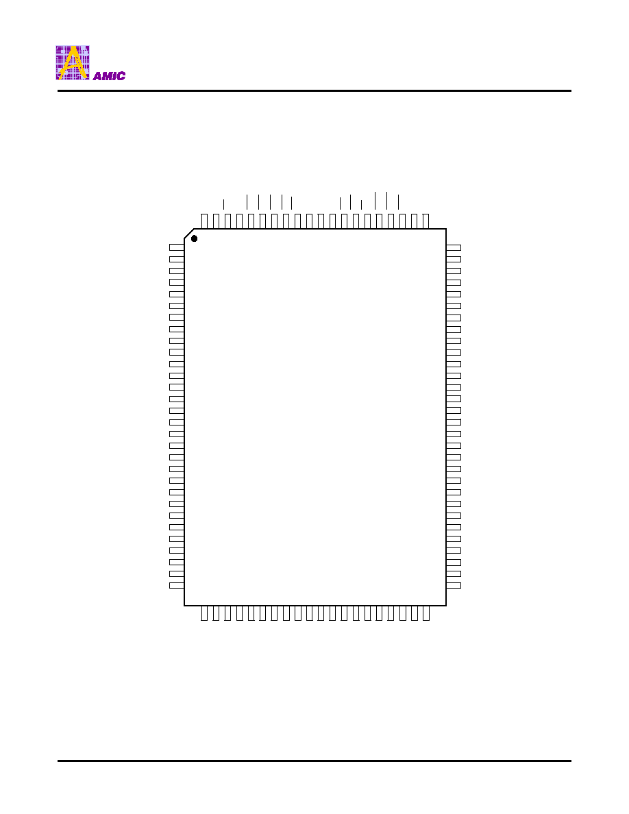
Pin Configuration
I/O
20
I/O
21
VCCQ
GNDQ
I/O
22
I/O
23
I/O
24
I/O
25
GNDQ
I/O
26
I/O
27
VCCQ
VCC
NC
I/O
34
GND
I/O
28
I/O
29
VCCQ
GNDQ
I/O
30
I/O
31
I/O
32
I/O
33
GNDQ
VCCQ
I/O
35
1
2
3
4
5
6
7
8
9
10
11
12
13
14
15
16
17
18
19
20
21
22
23
24
25
26
28
30
27
29
80
79
78
77
76
75
74
72
73
71
70
69
68
67
66
65
64
63
62
61
60
59
58
57
56
55
54
53
52
51
I/O
17
I/O
16
VCCQ
GNDQ
I/O
15
I/O
14
I/O
13
I/O
12
GNDQ
VCCQ
I/O
11
I/O
10
GND
NC
VCC
ZZ
I/O
8
I/O
7
VCCQ
GNDQ
I/O
6
I/O
5
I/O
4
I/O
3
GNDQ
VCCQ
I/O
2
I/O
1
50
49
48
47
46
45
44
43
42
40
41
39
38
37
36
35
34
33
32
31
A1
6
A1
5
A1
4
A1
3
A1
2
A1
1
A1
0
VCC
GN
D
NC
A0
A1
A2
A3
A4
A5
MO
D
E
81
82
83
84
85
86
87
88
89
90
91
92
93
94
95
96
97
98
99
10
0
CE
2
A7
A6
CL
K
GN
D
VCC
A9
A8
A63L83361E
NC
ADV
ADS
P
ADS
C
OE
BW
E
GW
CE
2
BW
1
BW
2
BW
3
BW
4
CE
A1
7
I/O
9
I/O
18
I/O
19
I/O
36
NC
NC
A63L83361
PRELIMINARY (July, 2005, Version 0.0)
3
AMIC Technology, Corp.
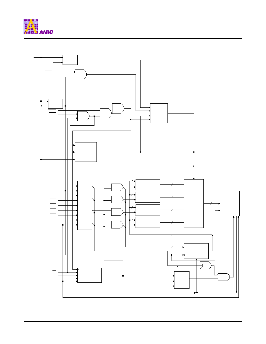
Block Diagram
MODE
LOGIC
CLK
LOGIC
ADDRESS
REGISTERS
BURST
LOGIC
ADDRESS
COUNTER
CLR
BYTE
WRITE
ENABLE
LOGIC
BYTE1
WRITE
DRIVER
BYTE2
WRITE
DRIVER
BYTE3
WRITE
DRIVER
BYTE4
WRITE
DRIVER
9
9
9
9
256KX9X4
MEMORY
ARRAY
9
9
9
9
36
OUTPUT
BUFFER
DATA-IN
REGISTERS
4
CHIP
ENABLE
LOGIC
OUTPUT
ENABLE
LOGIC
4
36
18
ZZ
MODE
ADV
CLK
ADSC
ADSP
A0-A17
GW
BWE
BW1
BW2
BW3
BW4
CE
CE2
CE2
OE
I/O
1
- I/O
36
A63L83361
PRELIMINARY (July, 2005, Version 0.0)
4
AMIC Technology, Corp.
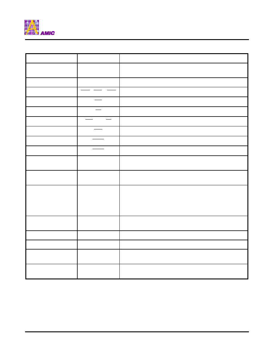
Pin Description
Pin No.
Symbol
Description
32 37 , 43 - 50, 81, 82,
99, 100
A0 - A17
Address Inputs
89 CLK
Clock
87, 93 - 96
BWE , BW1 - BW4
Byte Write Enables
88
GW
Global Write
86
OE
Output Enable
92, 97, 98
CE2 ,CE2, CE
Chip Enables
83
ADV
Burst Address Advance
84
ADSP
Processor Address Status
85
ADSC
Controller Address Status
31
MODE
Burst Mode: HIGH or NC (Interleaved burst)
LOW (Linear burst)
64
ZZ
Asynchronous Power-Down (Snooze): HIGH (Sleep)
LOW or NC (Wake up)
1,2, 3, 6 - 9, 12, 13, 18,
19, 22 - 25, 28, 29,30,51,
52, 53,
56 - 59, 62, 63, 68, 69, 72
- 75, 78, 79,80
I/O
1
- I/O
36
Data
Inputs/Outputs
1, 14, 16, 30, 38, 39, 42,
43, 51, 66, 80
NC No
Connection
15, 41, 65, 91
VCC
Power Supply
17, 40, 67, 90
GND
Ground
4, 11, 20, 27,
54, 61, 70, 77
VCCQ
Isolated Output Buffer Supply
5, 10, 21, 26,
55, 60, 71, 76
GNDQ
Isolated Output Buffer Ground