 | –≠–ª–µ–∫—Ç—Ä–æ–Ω–Ω—ã–π –∫–æ–º–ø–æ–Ω–µ–Ω—Ç: A63P73361 | –°–∫–∞—á–∞—Ç—å:  PDF PDF  ZIP ZIP |

A63P73361
128K X 36 Bit Synchronous High Speed SRAM with
Preliminary
Burst Counter and Flow-through Data Output
PRELIMINARY (July, 2005, Version 0.0)
AMIC Technology, Corp.
Document Title
128K X 36 Bit Synchronous High Speed SRAM with Burst Counter and Flow-
through Data Output
Revision History
Rev. No. History Issue
Date Remark
0.0
Initial issue
July 7, 2005
Preliminary

A63P73361
128K X 36 Bit Synchronous High Speed SRAM with
Preliminary
Burst Counter and Flow-through Data Output
PRELIMINARY (July, 2005, Version 0.0)
1
AMIC Technology, Corp.
Features
Fast access times: 6.5/7.5/8.0 ns(153/133/117 MHz)
Single 2.5V
±
5% power supply
Synchronous burst function
Individual Byte Write control and Global Write
Three separate chip enables allow wide range of
options for CE control, address pipelining
Selectable BURST mode
SLEEP mode (ZZ pin) provided
Available in 100-pin LQFP package
Industrial operating temperature range: -45
∞
C to
+125
∞
C for -I series
General Description
The A63P73361 is a high-speed SRAM containing 4.5M
bits of bit synchronous memory, organized as 128K
words by 36 bits.
The A63P73361 combines advanced synchronous
peripheral circuitry, 2-bit burst control, input registers,
output buffer and a 128K X 36 SRAM core to provide a
wide range of data RAM applications.
The positive edge triggered single clock input (CLK)
controls all synchronous inputs passing through the
registers. Synchronous inputs include all addresses (A0 -
A16), all data inputs (I/O
1
- I/O
36
), active LOW chip enable
(
CE ), two additional chip enables (CE2, CE2 ), burst
control inputs ( ADSC , ADSP , ADV ), byte write enables
( BWE , BW1 , BW2 , BW3 , BW4 ) and Global Write
( GW ). Asynchronous inputs include output enable ( OE ),
clock (CLK), BURST mode (MODE) and SLEEP mode
(ZZ).
Burst operations can be initiated with either the address
status processor ( ADSP ) or address status controller
( ADSC ) input pin. Subsequent burst sequence burst
addresses can be internally generated by the A63P73361
and controlled by the burst advance ( ADV ) pin. Write
cycles are internally self-timed and synchronous with the
rising edge of the clock (CLK).
This feature simplifies the write interface. Individual Byte
enables allow individual bytes to be written. BW1 controls
I/O
1
- I/O
9
, BW2 controls I/O
10
- I/O
18
, BW3 controls
I/O
19
- I/O
27
, and BW4 controls I/O
28
- I/O
36
, all on the
condition that BWE is LOW. GW LOW causes all bytes
to be written.
A63P73361
PRELIMINARY (July, 2005, Version 0.0)
2
AMIC Technology, Corp.
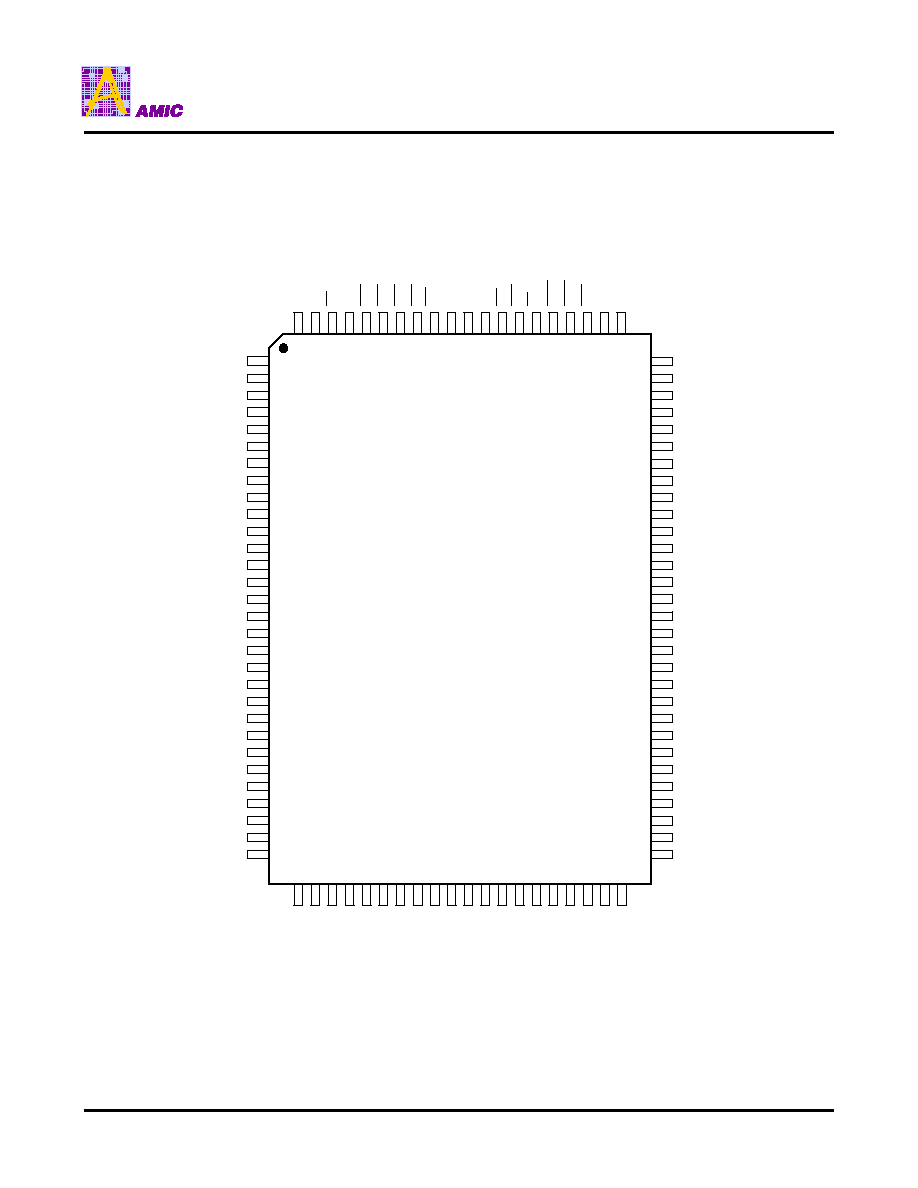
Pin Configuration
I/O
20
I/O
21
VCCQ
GNDQ
I/O
22
I/O
23
I/O
24
I/O
25
GNDQ
I/O
26
I/O
27
VCCQ
VCC
NC
I/O
34
GND
I/O
28
I/O
29
VCCQ
GNDQ
I/O
30
I/O
31
I/O
32
I/O
33
GNDQ
VCCQ
I/O
35
1
2
3
4
5
6
7
8
9
10
11
12
13
14
15
16
17
18
19
20
21
22
23
24
25
26
28
30
27
29
80
79
78
77
76
75
74
72
73
71
70
69
68
67
66
65
64
63
62
61
60
59
58
57
56
55
54
53
52
51
I/O
17
I/O
16
VCCQ
GNDQ
I/O
15
I/O
14
I/O
13
I/O
12
GNDQ
VCCQ
I/O
11
I/O
10
GND
NC
VCC
ZZ
I/O
8
I/O
7
VCCQ
GNDQ
I/O
6
I/O
5
I/O
4
I/O
3
GNDQ
VCCQ
I/O
2
I/O
1
50
49
48
47
46
45
44
43
42
40
41
39
38
37
36
35
34
33
32
31
A1
5
A1
4
A1
3
A1
2
A1
1
A1
0
NC
VCC
GN
D
NC
A0
A1
A2
A3
A4
A5
MO
D
E
81
82
83
84
85
86
87
88
89
90
91
92
93
94
95
96
97
98
99
10
0
CE
2
A7
A6
CL
K
GN
D
VCC
A9
A8
A63P73361E
NC
ADV
ADS
P
ADS
C
OE
BW
E
GW
CE
2
BW
1
BW
2
BW
3
BW
4
CE
A1
6
I/O
9
I/O
18
I/O
19
I/O
36
NC
NC

A63P73361
PRELIMINARY (July, 2005, Version 0.0)
3
AMIC Technology, Corp.
Block Diagram
MODE
LOGIC
CLK
LOGIC
ADDRESS
REGISTERS
BURST
LOGIC
ADDRESS
COUNTER
CLR
BYTE
WRITE
ENABLE
LOGIC
BYTE1
WRITE
DRIVER
BYTE2
WRITE
DRIVER
BYTE3
WRITE
DRIVER
BYTE4
WRITE
DRIVER
9
9
9
9
128KX9X4
MEMORY
ARRAY
9
9
9
9
36
OUTPUT
BUFFER
DATA-IN
REGISTERS
4
CHIP
ENABLE
LOGIC
OUTPUT
ENABLE
LOGIC
4
36
17
ZZ
MODE
ADV
CLK
ADSC
ADSP
A0-A16
GW
BWE
BW1
BW2
BW3
BW4
CE
CE2
CE2
OE
I/O
1
- I/O
36
A63P73361
PRELIMINARY (July, 2005, Version 0.0)
4
AMIC Technology, Corp.
Pin Description
Pin No.
Symbol
Description
32 ≠ 37, 44 - 50, 81, 82,
99, 100
A0 - A16
Address Inputs
89 CLK
Clock
87, 93 - 96
BWE , BW1 - BW4
Byte Write Enables
88
GW
Global Write
86
OE
Output Enable
92, 97, 98
CE2 ,CE2, CE
Chip Enables
83
ADV
Burst Address Advance
84
ADSP
Processor Address Status
85
ADSC
Controller Address Status
31
MODE
Burst Mode: HIGH or NC (Interleaved burst)
LOW (Linear burst)
64
ZZ
Asynchronous Power-Down (Snooze): HIGH (Sleep)
LOW or NC (Wake up)
1,2, 3, 6 - 9, 12, 13, 18,
19, 22 - 25, 28, 29,30,51,
52, 53,
56 - 59, 62, 63, 68, 69, 72
- 75, 78, 79,80
I/O
1
- I/O
36
Data
Inputs/Outputs
1, 14, 16, 30, 38, 39, 42,
43, 51, 66, 80
NC No
Connection
15, 41, 65, 91
VCC
Power Supply
17, 40, 67, 90
GND
Ground
4, 11, 20, 27,
54, 61, 70, 77
VCCQ
Isolated Output Buffer Supply
5, 10, 21, 26,
55, 60, 71, 76
GNDQ
Isolated Output Buffer Ground

A63P73361
PRELIMINARY (July, 2005, Version 0.0)
5
AMIC Technology, Corp.
Synchronous Truth Table (See Notes 1 Through 5)
Operation
Address
Used
CE
CE2
CE2
ADSP
ADSC
ADV
WRITE
OE
CLK
I/O
Operation
Deselected Cycle,
Power-down
NONE H X X X L X X X
L-H High-Z
Deselected Cycle,
Power-down
NONE L X L L X X X X
L-H High-Z
Deselected Cycle,
Power-down
NONE L H X L X X X X
L-H High-Z
Deselected Cycle,
Power-down
NONE L X L H L X X X
L-H High-Z
Deselected Cycle,
Power-down
NONE L H X H L X X X
L-H High-Z
READ Cycle,
Begin Burst
External
L
L
H L X X X L
L-H Dout
READ Cycle,
Begin Burst
External
L L H L X X X H
L-H High-Z
WRITE Cycle,
Begin Burst
External
L L H H L X L X
L-H Din
READ Cycle,
Begin Burst
External
L L H H L X H L
L-H Dout
READ Cycle,
Begin Burst
External
L L H H L X H H
L-H High-Z
READ Cycle,
Continue Burst
Next X X X H H L H L
L-H Dout
READ Cycle,
Continue Burst
Next X X X H H L H H
L-H High-Z
READ Cycle,
Continue Burst
Next H X X X H L H L
L-H Dout
READ Cycle,
Continue Burst
Next H X X X H L H H
L-H High-Z
WRITE Cycle,
Continue Burst
Next X X X H H L L X
L-H Din
WRITE Cycle,
Continue Burst
Next H X X X H L L X
L-H Din
READ Cycle,
Suspend Burst
Current X X X H H H H L
L-H Dout
READ Cycle,
Suspend Burst
Current X X X H H H H H
L-H High-Z
READ Cycle,
Suspend Burst
Current H X X X H H
H L L-H
Dout
READ Cycle,
Suspend Burst
Current H X X X H H
H H L-H High-Z
WRITE Cycle,
Suspend Burst
Current X X X H H H L X
L-H Din
WRITE Cycle,
Suspend Burst
Current H X X X H H
L X L-H
Din
A63P73361
PRELIMINARY (July, 2005, Version 0.0)
6
AMIC Technology, Corp.
Notes: 1. X = "Disregard", H = Logic High, L = Logic Low.
2.
WRITE = L means:
1)
Any
BWx ( BW1, BW2 , BW3 , or BW4 ) and BWE are low or
2)
GW is low.
3. All inputs except OE must be synchronized with setup and hold times around the rising edge (L-H) of CLK.
4. For write cycles that follow read cycles, OE must be HIGH before the input data request setup time and held
HIGH throughout the input data hold time.
5.
ADSP LOW always initiates an internal Read at the L-H edge of CLK. A Write is performed by setting one or
more byte write enable signals and BWE LOW or GW LOW for the subsequent L-H edge of CLK. Refer to
the Write timing diagram for clarification.
Write Truth Table
Operation
GW
BWE
BW1
BW2
BW3
BW4
READ
H H X X X X
READ
H L H H H H
WRITE Byte 1
H
L
L
H
H
H
WRITE
all
bytes
H L L L L L
WRITE
all
bytes
L X X X X X
A63P73361
PRELIMINARY (July, 2005, Version 0.0)
7
AMIC Technology, Corp.
Linear Burst Address Table (MODE = LOW)
First Address (External)
Second Address (Internal)
Third Address (Internal)
Fourth Address (Internal)
X . . . X00
X . . . X01
X . . . X10
X . . . X11
X . . . X01
X . . . X10
X . . . X11
X . . . X00
X . . . X10
X . . . X11
X . . . X00
X . . . X01
X . . . X11
X . . . X00
X . . . X01
X . . . X10
Interleaved Burst Address Table (MODE = HIGH or NC)
First Address (External)
Second Address (Internal)
Third Address (Internal)
Fourth Address (Internal)
X . . . X00
X . . . X01
X . . . X10
X . . . X11
X . . . X01
X . . . X00
X . . . X11
X . . . X10
X . . . X10
X . . . X11
X . . . X00
X . . . X01
X . . . X11
X . . . X10
X . . . X01
X . . . X00
Absolute Maximum Ratings*
Power Supply Voltage (VCC) . . . . . . . . . . -0.5V to +3.6V
Voltage Relative to GND for any Pin Except VCC (Vin,
Vout) . . . . . . . . . . . . . . . . . . . . . . . . . -0.5V to VCC +0.5V
Power Dissipation (P
D
) . . . . . . . . . . . . . . . . . . . . . . . . 2W
Storage Temperature (Tbias) . . . . . . . . . . -65
∞
C to 150
∞
C
Storage Temperature (Tstg) . . . . . . . . . . . -55
∞
C to 125
∞
C
Operating Ranges
Ambient Temperature
Commercial (C) Devices . . . . . . . . . . . . . . . 0
∞
C to +70
∞
C
Industrial (I) Devices . . . . . . . . . . . . . . . -45
∞
C to +125
∞
C
V
CC
& V
CCQ
Supply Voltages
V
CC
for all devices . . ..... . . . . . . . . . . . . . . . . . . . +2.5V
V
CCQ
for all devices . . ..... . . . . . . . . . . . . . . . . . . +2.5V
Operating ranges define those limits between which the
functionally of the device is guaranteed.
*Comments
Stresses above those listed under "Absolute Maximum
Ratings" may cause permanent damage to this device.
These are stress ratings only. Functional operation of
this device at these or any other conditions above those
indicated in the operational sections of this specification
is not implied or intended. Exposure to the absolute
maximum rating conditions for extended periods may
affect device reliability.
Recommended DC Operating Conditions
(0
∞
C
T
A
70
∞
C, VCC, VCCQ = 2.5V+5% or 2.5V-5%, unless otherwise noted)
Symbol Parameter Min.
Typ.
Max.
Unit
Note
VCC
Supply Voltage (Operating Voltage Range)
2.375
2.5
2.625
V
VCCQ
Isolated Input Buffer Supply
2.375
2.5
2.625
V
GND
Supply Voltage to GND
0.0
-
0.0
V
V
IH
Input High Voltage
1.7
-
VCC+0.3
V
1, 2
V
IHQ
Input High Voltage (I/O Pins)
1.7
-
VCC+0.3
V
V
IL
Input Low Voltage
-0.3
-
0.7
V
1, 2

A63P73361
PRELIMINARY (July, 2005, Version 0.0)
8
AMIC Technology, Corp.
DC Electrical Characteristics
(0
∞
C
T
A
70
∞
C, VCC, VCCQ = 2.5V+5% or 2.5V-5%, unless otherwise noted)
Symbol Parameter Min.
Max.
Unit Test
Conditions Note
I
LI
Input Leakage Current
-
±
2.0
µ
A
All inputs V
IN
= GND to VCC
I
LO
Output Leakage Current
-
±
2.0
µ
A
OE = V
IH
, Vout = GND to VCC
I
CC1
Supply Current
-
300
mA
Device selected; VCC = max.
Iout = 0mA, all inputs = V
IH
or V
IL
Cycle time = t
KC
min.
3, 11
I
SB1
Standby Current
-
30
mA
Device deselected; VCC = max.
All inputs are fixed.
All inputs
VCC - 0.2V
or
GND + 0.2V
Cycle time = t
KC
min.
11
I
SB2
- 15 mA
ZZ
VCC - 0.2V
V
OL
Output Low Voltage
-
0.4
V
I
OL
= 1 mA
V
OH
Output High Voltage
2.0
-
V
I
OH
= -1 mA
Capacitance
Symbol Parameter
Typ.
Max.
Unit
Conditions
C
IN
Input
Capacitance
3
4
pF
T
A
= 25 C; f = 1MHz
C
I/O
Input/Output
Capacitance
4 5
pF
VCC = 2.5V
* These parameters are sampled and not 100% tested.

A63P73361
PRELIMINARY (July, 2005, Version 0.0)
9
AMIC Technology, Corp.
AC Characteristics
(0
∞
C
T
A
70
∞
C, VCC = 2.5V+5% or 2.5V-5%)
Symbol Parameter
-6.5 -7.5 -8.5
Unit
Note
Min.
Max.
Min.
Max.
Min.
Max.
T
KC
Clock Cycle Time
7.5
-
8.5
-
10
-
ns
T
KH
Clock High Time
2.5
-
2.8
-
3.0
-
ns
T
KL
Clock Low Time
2.5
-
2.8
-
3.0
-
ns
T
KQ
Clock to Output Valid
-
6.5
-
7.5
-
8.5
ns
t
KQX
Clock to Output Invalid
3.0
-
3.0
-
3.0
-
ns
t
KQLZ
Clock to Output in Low-Z
2.5
-
2.5
-
2.5
-
ns
5, 6
t
KQHZ
Clock to Output in High-Z
-
3.5
-
3.5
-
5.0
ns
5, 6
t
OEQ
OE to Output Valid
- 3.5 - 3.5 - 5.0 ns 8
t
OELZ
OE to Output in Low-Z
0 - 0 - 0 - ns
5,
6
t
OEHZ
OE to Output in High-Z
- 3.5 - 3.5 - 5.0 ns 5,
6
Setup Times
T
AS
Address
1.5 - 2.0 - 2.0 - ns 7,
9
t
ADSS
Address Status ( ADSC , ADSP )
1.5 - 2.0 - 2.0 - ns 7,
9
t
ADVS
Address Advance ( ADV )
1.5 - 2.0 - 2.0 - ns 7,
9
t
WS
Write Signals
( BW1, BW2 , BW3 , BW4 , BWE , GW )
1.5 - 2.0 - 2.0 - ns 7,
9
T
DS
Data-in
1.5 - 1.5 - 2.0 - ns 7,
9
t
CES
Chip Enable ( CE , CE2, CE2 )
1.5 - 2.0 - 2.0 - ns 7,
9
Hold Times
T
AH
Address
0.5 0.5 0.5 ns 7,
9
t
ADSH
Address Status ( ADSC , ADSP )
0.5 0.5 0.5 ns 7,
9
t
AAH
Address Advance ( ADV )
0.5 0.5 0.5 ns 7,
9
t
WH
Write Signal
( BW1, BW2 , BW3 , BW4 , BWE , GW )
0.5 0.5 0.5 ns 7,
9
T
DH
Data-in
0.5 0.5 0.5 ns 7,
9
t
CEH
Chip Enable ( CE , CE2, CE2 )
0.5 0.5 0.5 ns 7,
9

A63P73361
PRELIMINARY (July, 2005, Version 0.0)
10
AMIC Technology, Corp.
Notes:
1. All voltages refer to GND.
2. Overshoot: V
IH
+2V for t
t
KC
/2.
Undershoot:
V
IL
-0.7V for t
t
KC
/2.
Power-up: V
IH
+2 and VCC
1.7V
for
t
200ms
3. I
CC1
is given with no output current. I
CC1
increases with greater output loading and faster cycle times.
4. Test conditions assume the output loading shown in Figure 1, unless otherwise specified.
5. For output loading, C
L
= 5pF, as shown in Figure 2. Transition is measured
±
150mV from steady state voltage.
6. At any given temperature and voltage condition, t
KQHZ
is less than t
KQLZ
and t
OEHZ
is less than t
QELZ
.
7. A WRITE cycle is defined by at least one Byte Write enable LOW and ADSP HIGH for the required setup and hold
times. A READ cycle is defined by all byte write enables HIGH and ( ADSC or ADV LOW) or ADSP LOW for the
required setup and hold times.
8. OE has no effect when a Byte Write enable is sampled LOW.
9. This is a synchronous device. All addresses must meet the specified setup and hold times for all rising edges of CLK
when
either
ADSP or ADSC is LOW and the chip is enabled. All other synchronous inputs must meet the setup and
hold times with stable logic levels for all rising edges of clock (CLK) when the chip is enabled. Chip enable must be
valid at each rising edge of CLK when either ADSP or ADSC is LOW to remain enabled.
10. The load used for V
OH
, V
OL
testing is shown in Figure 2. AC load current is higher than the given DC values.
AC I/O curves are available upon request.
11. "Device Deselected" means device is in POWER-DOWN mode, as defined in the truth table. "Device Selected" means
device is active (not in POWER-DOWN mode).
12. MODE pin has an internal pulled-up, and ZZ pin has an internal pulled-down. All of then exhibit an input leakage
current of 10
µ
A.
13. Snooze (ZZ) input is recommended that users plan for four clock cycles to go into SLEEP mode and four clocks to
emerge from SLEEP mode to ensure no data is lost.
A63P73361
PRELIMINARY (July, 2005, Version 0.0)
11
AMIC Technology, Corp.
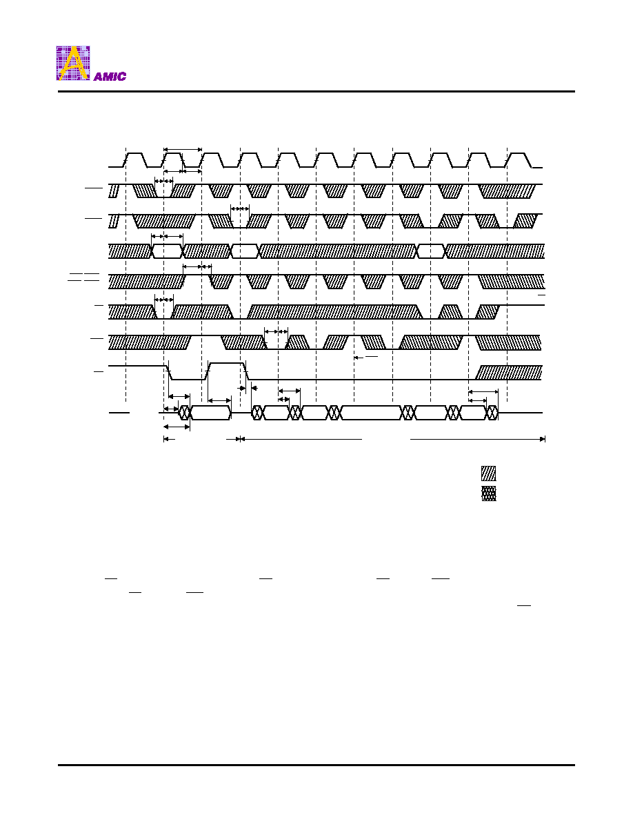
Timing Waveforms
Read Timing
Notes: 1. QA(2) refers to output from address A2. Q(A2+1) refers to output from the next internal burst address following A2.
2.
CE and CE2 have timing identical to CE . On this diagram, when CE is LOW, CE2 is LOW and CE2 is HIGH.
When CE is HIGH, CE2 is HIGH and CE2 is LOW.
3. Timing is shown assuming that the device was not enabled before entering into this sequence. OE does not
cause Q to be driven until after the following clock rising edge.
CLK
ADSP
ADSC
ADDRESS
A1
A2
GW,BWE
BW1-BW4
CE
(NOTE 2)
ADV
OE
Q(A1)
Q(A2)
Q(A2+1)
Q(A2+2)
High-Z
DOUT
(NOTE 3)
t
OEHZ
t
KQX
t
KQ
t
KQX
BURST READ
Deselect cycle
ADV suspends burst
t
ADVH
t
ADVS
t
CEH
t
CES
t
WH
t
WS
t
AH
t
AS
t
ADSH
t
ADSS
t
ADSH
t
ADSS
t
KL
t
KH
t
KC
(NOTE *1)
t
OEQ
t
KQLZ
t
KQ
t
OELZ
Single READ
Don't Care
Undefined
A3
Q(A2+3)
Q(A3)
t
KQHZ
Deselect with CE

A63P73361
PRELIMINARY (July, 2005, Version 0.0)
12
AMIC Technology, Corp.
Timing Waveforms (continued)
CLK
ADSP
ADSC
ADDRESS
A1
A2
A3
OE
D(A2)
D(A2+1)
D(A2+2)
D(A2+3)
D(A3)
D(A3+1)
High-Z
DIN
t
AH
t
AS
t
ADSH
t
ADSS
t
ADSH
t
ADSS
t
KL
t
KH
t
KC
t
ADSH
t
ADSS
ADSC extends burst
GW
CE
(NOTE 2)
ADV
D(A1)
D(A2+1)
D(A3+2)
DOUT
BURST READ
Single WRITE
Extended BURST WRITE
t
OEHZ
t
DH
t
DS
(NOTE 3)
(NOTE 4)
ADV suspends burst
t
ADVH
t
ADVS
t
CEH
t
CES
t
WH
t
WS
BYTE WRITE signals are ignored
for first cycle when ADSP initiates burst
t
WH
t
WS
BWE,BW1-BW4
(NOTE 5)
(NOTE 1)
Don't Care
Undefined
Write Timing
Notes: 1. D(A2) refers to output from address A2. D(A2+1) refers to output from the internal burst address immediately
following A2.
2.
Timing
for
CE2 and CE2 is identical to that for CE . As shown in the above diagram, when CE is LOW, CE2
is LOW and CE2 is HIGH. When CE is HIGH, CE2 is HIGH and CE2 is LOW.
3.
OE must be HIGH before the input data setup, and held HIGH throughout the data hold period. This prevents
input/output data contention for the period prior to the time Byte Write enable inputs are sampled.
4.
ADV must be HIGH to permit a Write to the loaded address.
5. Byte Write enables are decided by means of a Write truth table.

A63P73361
PRELIMINARY (July, 2005, Version 0.0)
13
AMIC Technology, Corp.
Timing Waveforms (continued)
Read/Write Timing
Notes: 1. Q(A4) refers to output from address A4. Q(A4+1) refers to output from the next internal burst address following A4.
2.
CE2 and CE2 have timing identical to CE . On this diagram, when CE is LOW, CE is LOW and CE2 is HIGH,
When CE is HIGH, CE2 is HIGH and CE2 is LOW.
3. The data bus (Q) remains in High-Z following a WRITE cycle unless an ADSP , ADSC , or ADV cycle is
performed.
4. Byte Write enables are decided by means of a Write truth table.
5. Back-to-back READs may be controlled by either ADSP or ADSC
CLK
ADSP
ADSC
ADDRESS
A1
A3
CE
(NOTE 2)
ADV
OE
D(A3)
D(A5)
D(A6)
High-Z
DIN
t
CEH
t
CES
t
ADSH
t
ADSS
t
KL
t
KH
t
KC
A2
A4
A5
A6
GW,BWE,
BW1-BW4
(NOTE 3)
Q(A1)
Q(A2)
Q(A4)
Q(A4+1)
DOUT
Back-to-Back READs
Single WRITE
BURST READ
Back-to-Back
WRITEs
(NOTE 1)
t
KQ
t
OELZ
t
DH
t
DS
t
WS
t
WH
t
AS
t
AH
Q(A4+2)
Q(A4+3)
t
OEHZ
t
KQ
Don't Care
Undefined

A63P73361
PRELIMINARY (July, 2005, Version 0.0)
14
AMIC Technology, Corp.
AC Test Conditions
Input Pulse Levels
GND to 3V
Input Rise and Fall Times
1 ns
Input Timing Reference Levels
1.5V
Output Reference Levels
VccQ/2
Output Load
See Figures 1 and 2
Figure 1. Output Load Equivalent Figure
Z
O
=50
Q
R
L
=50
V
T
=0.75V
2. Output Load Equivalent
Q
VCCQ/2
50
5pF
Ordering Information
Part No.
Access Times (ns)
Frequency (MHz)
Package
A63P73361E-6.5 6.5
153 100L
LQFP
A63P73361E-6.5F
6.5
153
100L Pb-Free LQFP
A63P73361E-7.5 7.5
133 100L
LQFP
A63P73361E-7.5F
7.5
133
100L Pb-Free LQFP
A63P73361E-8 8
117
100L
LQFP
A63P73361E-8F
8
117
100L Pb-Free LQFP

A63P73361
PRELIMINARY (July, 2005, Version 0.0)
15
AMIC Technology, Corp.
Package Information
LQFP 100L Outline Dimensions
unit: inches/mm
Symbol
Dimensions in inches
Dimensions in mm
Min.
Nom.
Max.
Min.
Nom.
Max.
A
1
0.002
- - 0.05 - -
A
2
0.053
0.055
0.057
1.35
1.40
1.45
b 0.011
0.013
0.015
0.27
0.32
0.37
c 0.005
-
0.008
0.12 - 0.20
H
E
0.860
0.866
0.872
23.35
22.00
22.15
E 0.783
0.787
0.791
19.90
20.00
20.10
H
D
0.624
0.630
0.636
15.85
16.00
16.15
D 0.547
0.551
0.555
13.90
14.00
14.10
e
0.026 BSC
0.65 BSC
L 0.018
0.024
0.030
0.45
0.60
0.75
L
1
0.039 REF
1.00 REF
y -
-
0.004
-
-
0.1
0
∞
3.5
∞
7
∞
0
∞
3.5
∞
7
∞
Notes:
1. Dimensions D and E do not include mold protrusion.
2. Dimensions b does not include dambar protrusion.
Total in excess of the b dimension at maximum material condition.
Dambar cannot be located on the lower radius of the foot.
31
50
51
80
81
100
H
D
D
E
H
E
1
30
b
D y
A
1
A
2
L
1
c
e
L