A64S9316
Preliminary
512K X 16 Bit Low Voltage Super RAM
TM
PRELIMINARY
(July, 2002, Version 0.1)
AMIC Technology, Inc.
Document Title
512K X 16 Bit Low Voltage Super RAM
TM
Revision History
Rev. No. History
Issue Date
Remark
0.0
Initial issue
May 16, 2002
Preliminary
0.1
Add t
ASC
, t
AHC
, t
CEH
, t
WEH
July 31, 2002

A64S9316
Preliminary
512K X 16 Bit Low Voltage Super RAM
TM
PRELIMINARY
(July, 2002, Version 0.1)
1
AMIC Technology, Inc.
Features
n
Operating voltage: 2.7V to 3.1V
n
Access times: 70 ns (max.)
n
Current:
A64S9316 series: Operating: 35mA (max.)
Power Down Standby: 10
µ
A (max.)
n
Fully SRAM compatible operation
n
Full static operation, no clock or refreshing required
n
All inputs and outputs are directly TTL-compatible
n
Common I/O using three-state output
n
Industrial operating temperature range: -25
∞
C to +85
∞
C
for -I
n
Available in 48-ball Mini BGA (6X8) package.
General Description
The A64S9316 is a low operating current 8,388,608-bit
Super RAM organized as 524,288 words by 16 bits and
operates on low power supply voltage from 2.7V to 3.1V.
It is built using AMIC's high performance CMOS DRAM
process.
Using hidden refresh technique, the A64S9316 provides
a 100% compatible asynchronous interface.
Inputs and three-state outputs are TTL compatible and allow
for direct interfacing with common system bus structures.
The chip enable input is provided for POWER-DOWN,
device enable. Two byte enable inputs and an output enable
input are included for easy interfacing.
This A64S9316 is suited for low power application such as
mobile phone and PDA or other battery-operated handheld
device.
Pin Configuration
n
Mini BGA (6X8) Top View
1
2
3
4
5
6
A
LB
OE
A0
A1
A2
CE2
B
I/O
8
HB
A3
A4
CE1
I/O
0
C
I/O
9
I/O
10
A5
A6
I/O
1
I/O
2
D
VSS
I/O
11
A17
A7
I/O
3
VCC
E
VCC
I/O
12
GND
A16
I/O
4
VSS
F
I/O
14
I/O
13
A14
A15
I/O
5
I/O
6
G
I/O
15
NC
A12
A13
WE
I/O
7
H
A18
A8
A9
A10
A11
NC
A64S9316G
A64S9316
PRELIMINARY
(July, 2002, Version 0.1)
2
AMIC Technology, Inc.
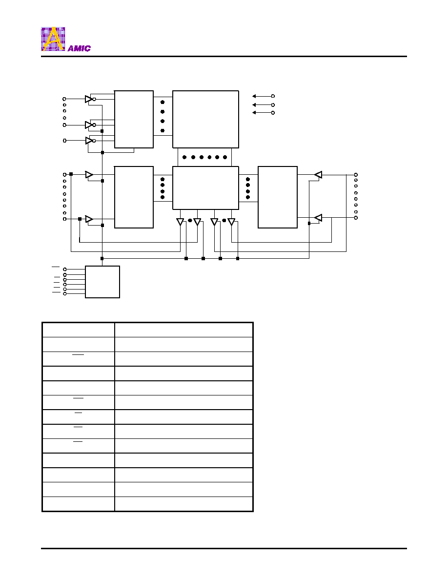
Block Diagram
DECODER
8,388,608
MEMORY ARRAY
COLUMN I/O
INPUT
DATA
CIRCUIT
CONTROL
CIRCUIT
VCC
GND
I/O
7
I/O
0
A18
A17
A0
WE
HB
INPUT
DATA
CIRCUIT
I/O
8
I/O
15
CE2
LB
OE
CE1
VSS
Pin Description
Symbol
Description
A0 - A18
Address Inputs
CE1
Chip Enable 1 Input
CE2
Chip Enable 2 Input
I/O
0
- I/O
15
Data Input/Outputs
WE
Write Enable Input
LB
Byte Enable Input (I/O
0
to I/O
7
)
HB
Byte Enable Input (I/O
8
to I/O
15
)
OE
Output Enable Input
VCC
Power
VSS
Ground
GND
Ground
NC
No Connection

A64S9316
PRELIMINARY
(July, 2002, Version 0.1)
3
AMIC Technology, Inc.
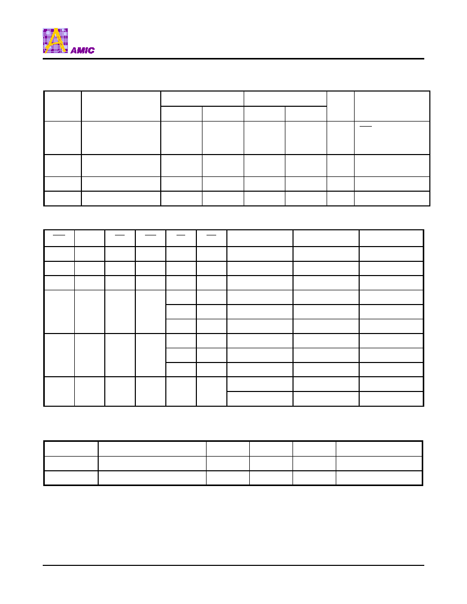
Recommended DC Operating Conditions
(T
A
= 0
∞
C to + 70
∞
C or -25
∞
C to 85
∞
C)
Symbol
Parameter
Min.
Max.
Unit
VCC
Supply Voltage
2.7
3.1
V
VSS
Ground
0
0
V
GND
Ground
0
0
V
V
IH
Input High Voltage
2.4
VCC + 0.3
V
V
IL
Input Low Voltage
-0.3
+0.6
V
C
L
Output Load
-
30
pF
TTL
Output Load
-
1
-
Absolute Maximum Ratings*
VCC to GND . . . . . . . . . . . . . . . . . . . . . -0.5V to +4.6V
IN, IN/OUT Volt to GND . . . . . . . . -0.5V to VCC + 0.5V
Storage Temperature, Tstg . . . . . . . . . -55
∞
C to +125
∞
C
Power Dissipation, P
T
. . . . . . . . . . . . . . . . . . . . . 0.7W
Soldering Temp. & Time . . . . . . . . . . . . 260
∞
C, 10 sec
*Comments
Stresses above those listed under "Absolute Maximum
Ratings" may cause permanent damage to this device.
These are stress ratings only. Functional operation of this
device at these or any other conditions above those
indicated in the operational sections of this specification
is not implied or intended. Exposure to the absolute
maximum rating conditions for extended periods may
affect device reliability.
DC Electrical Characteristics
(T
A
= 0
∞
C to + 70
∞
C or -25
∞
C to 85
∞
C, VCC = 2.7V to 3.1V, GND = 0V)
Symbol
Parameter
-70
-85
Unit
Conditions
Min.
Max.
Min.
Max.
I
LI
Input Leakage
Current
-
1
-
1
µ
A
V
IN
= GND to VCC
I
LO
Output Leakage
Current
-
1
-
1
µ
A
CE1 = V
IH
or CE2 = V
IL
or
OE = V
IH
or WE = V
IL
V
I/O
= GND to VCC
I
CC1
-
35
-
30
mA
Min. Cycle, Duty = 100%
CE1 = V
IL
, CE2 = V
IH
I
I/O
= 0mA
I
CC2
Dynamic Operating
Current
-
5
-
5
mA
CE1 = V
IL
, CE2 = V
IH
V
IH
= VCC, V
IL
= 0V,
f = 1MHz, I
I/O
= 0mA
A64S9316
PRELIMINARY
(July, 2002, Version 0.1)
4
AMIC Technology, Inc.
DC Electrical Characteristics
(continued)
Symbol
Parameter
-70
-85
Unit
Conditions
Min.
Max.
Min.
Max.
I
SB1
Standby Power
Supply Current
-
80
-
80
µ
A
CE1
VCC - 0.2V
CE2
VCC - 0.2V
V
IN
0V
I
SB2
Power Down Mode
Standby Current
-
10
-
10
µ
A
CE2
0.2V
V
OL
Output Low Voltage
-
0.4
-
0.4
V
I
OL
= 2.1mA
V
OH
Output High Voltage
2.4
-
2.4
-
V
I
OH
= -1.0mA
Truth Table
CE1
CE2
OE
WE
LB
HB
I/O
0
to I/O
7
Mode
I/O
8
to I/O
15
Mode
VCC Current
H
H
X
X
X
X
Not selected
Not selected
I
SB1
, I
SB
X
H
X
X
H
H
Not selected
Not selected
I
SB1
, I
SB
X
L
X
X
X
X
Not selected
Not selected
I
SB2
L
L
Read
Read
I
CC1
, I
CC2
L
H
L
H
L
H
Read
High - Z
I
CC1
, I
CC2
H
L
High - Z
Read
I
CC1
, I
CC2
L
L
Write
Write
I
CC1
, I
CC2
L
H
X
L
L
H
Write
Not Write/Hi - Z
I
CC1
, I
CC2
H
L
Not Write/Hi - Z
Write
I
CC1
, I
CC2
High - Z
High - Z
I
CC1
, I
CC2
L
H
H
H
X
X
High - Z
High - Z
I
CC1
, I
CC2
Note: X = H or L
Capacitance
(T
A
= 25
∞
C, f = 1.0MHz)
Symbol
Parameter
Min.
Max.
Unit
Conditions
C
IN
*
Input Capacitance
-
10
pF
V
IN
= 0V
C
I/O
*
Input/Output Capacitance
-
10
pF
V
I/O
= 0V
* These parameters are sampled and not 100% tested.