
A65H73361/A65H83181 Series
128K x 36 & 256K x 18 Late Write Synchronous
Preliminary
Fast SRAM with Pipelined Data Output
PRELIMINARY (
February, 1999, Version 2.0)
AMIC Technology, Inc.
Document Title
128K x 36 & 256K x 18 Late Write Synchronous Fast SRAM with Pipelined Data Output
Revision History
Rev. No.
History
Issue Date
Remark
2.0
Add JTAG standard
February 12, 1999
Preliminary

A65H73361/A65H83181 Series
128K x 36 & 256K x 18 Late Write Synchronous
Preliminary
Fast SRAM with Pipelined Data Output
PRELIMINARY (
February, 1999, Version 2.0)
1
AMIC Technology, Inc.
Features
n
Fast access times: 2.5/3.0/3.5ns
n
128k x 36 or 256k x 18 organizations
n
CMOS technology
n
Register to register synchronous operation with self-
timed late write
n
Single +3.3V
±
5% power supply
n
Individual byte write and global write
n
HSTL input & output levels
n
Boundary scan(JTAG) IEEE 1149.1 compatible
n
Asynchronous output enable
n
Sleep mode (ZZ)
n
Programmable impedance output drivers
n
JEDEC Standard pinout and boundary scan order
n
7 x 17 bump plastic ball grid array (PBGA) package
General Description
The A65H73361 and A65H83181 are 128k words by 36
bits and 256k words by 18 bits late write synchronous
4Mb SRAMS built using high performance CMOS
process.
The differential clock are used to control the timing of
read/write operation and all internal operations are self-
timed. The positive edge triggered CK clock input
controls all addresses write-enables and Synchronous
select and data ins are registered.
The data outs are controlled by the output registers off
the next positive clock edge to be updated.
The internal write buffer enables write data to be
accepted on the rising edge of the clock one cycle after
address and control signals.
The SRAM uses HSTL I/O interfaces with programmable
impedance output drivers allowing the outputs to match
the impedance of the circuit traces which reduces signal
reflections.
A65H73361/A65H83181 Series
PRELIMINARY
(February, 1999, Version 2.0)
2
AMIC Technology, Inc.
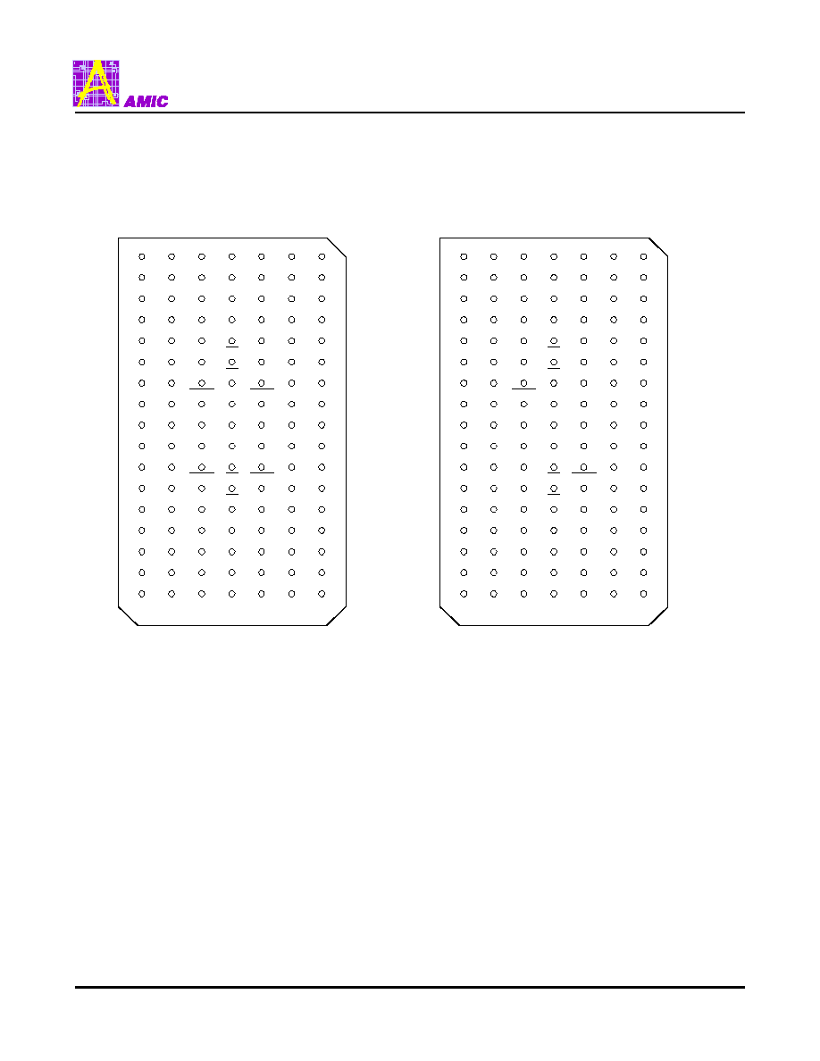
Pin Configuration
A65H73361
V
DDQ
SA
7
NC
SA
16
SA
14
V
DDQ
1
2
3
4
5
6
7
NC
NC
SA
8
NC
SA
11
NC
NC
NC
SA
6
SA
9
V
DD
SA
10
SA
15
NC
DQ
18
DQ
27
V
SS
NC
M
1
V
DD
NC
NC
ZZ
V
DDQ
TMS
TDI
TCK
TDO
NC
A
B
C
D
E
F
G
H
J
K
L
M
N
P
R
T
U
V
DDQ
NC
NC
M
2
V
SS
SA
5
DQ
19
SA
4
SA
12
SA
3
SA
2
SA
13
SA
1
DQ
1
DQ
0
DQ
3
DQ
2
V
DDQ
SW
V
SS
DQ
4
V
DDQ
DQ
32
DQ
33
SBW
d
CK
SBW
a
DQ
6
DQ
5
DQ
34
DQ
35
V
SS
CK
V
SS
DQ
8
DQ
7
V
DDQ
V
DD
V
ref
V
DD
V
ref
V
DD
V
DDQ
DQ
25
DQ
26
NC
V
SS
DQ
17
DQ
16
DQ
23
DQ
24
SBW
C
NC
SBW
b
DQ
15
DQ
14
V
DDQ
DQ
22
V
SS
G
V
SS
DQ
13
V
DDQ
DQ
20
DQ
21
V
SS
SS
V
SS
DQ
12
DQ
11
V
SS
ZQ
V
SS
DQ
10
DQ
9
DQ
31
DQ
30
DQ
25
V
SS
DQ
29
V
SS
V
SS
SA
0
A65H83181
V
DDQ
SA
7
NC
SA
16
SA
14
V
DDQ
1
2
3
4
5
6
7
NC
NC
SA
8
NC
SA
11
NC
NC
NC
SA
6
SA
9
V
DD
SA
10
SA
15
NC
DQ
9
NC
V
SS
NC
M
1
V
DD
NC
ZZ
V
DDQ
TMS
TDI
TCK
TDO
NC
A
B
C
D
E
F
G
H
J
K
L
M
N
P
R
T
U
V
DDQ
NC
M
2
V
SS
SA
5
NC
SA
4
SA
13
SA
3
NC
SA
17
SA
1
NC
DQ
0
DQ
3
NC
V
DDQ
SW
V
SS
NC
V
DDQ
DQ
14
NC
CK
SBW
a
DQ
6
NC
NC
DQ
17
V
SS
CK
V
SS
NC
DQ
7
V
DDQ
V
DD
V
ref
V
DD
V
ref
V
DD
V
DDQ
DQ
16
NC
NC
V
SS
DQ
8
NC
NC
DQ
15
SBW
b
NC
NC
DQ
5
V
DDQ
NC
V
SS
G
V
SS
DQ
4
V
DDQ
NC
DQ
12
V
SS
SS
V
SS
NC
DQ
2
V
SS
ZQ
V
SS
DQ
1
NC
DQ
13
NC
DQ
10
V
SS
DQ
11
V
SS
V
SS
SA
0
V
SS
V
SS
V
SS
SA
2
SA
12
V
SS
A65H73361/A65H83181 Series
PRELIMINARY
(February, 1999, Version 2.0)
3
AMIC Technology, Inc.
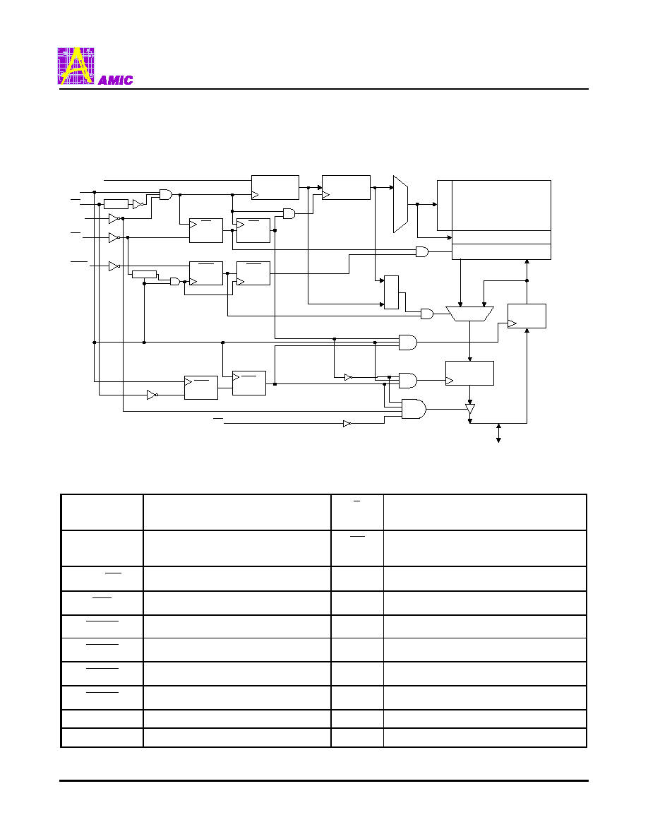
Block Diagram
128Kx36
or
256Kx18
Array
DQ0 - DQ35
Column Decoder
Read/Write Amp
Row Decoder
Write
Buffer
2:1 MUX
2:1 MUX
Match
WR Add
Register
Data Out
Registor
RD Add
Register
SW
Register
SBW
Register
SW
Register
SBW
Register
SA0-SA17
CK
Latch
SS
ZZ
SW
SBW
Latch
SS
Register
SS
Register
G
Pin Description
SA0-SA17
Address input
(X18 : SA0 - SA17, X36 : SA0 - SA16)
G
Asynchronous output enable
DQ0-DQ35
Data I/O
(X18 : DQ0 - DQ17, X36 : DQ0 - DQ35)
SS
Synchronous select
CK
,
CK
Differential input register clocks
M1, M2
For boundary scan purpose
SW
Write enable. Global
V
REP
(2)
HSTL input reference voltage
SBWa
Write enable. Byte a (DQ0-DQ8)
V
DD
Power supply (+3.3V)
SBWb
Write enable. Byte b (DQ9-DQ17)
V
SS
Ground
SBWc
Write enable. Byte c (DQ18-DQ26)
V
DDQ
Output power supply
SBWd
Write enable. Byte d (DQ27-DQ35)
ZZ
Asynchronous sleep mode
TMS, TDI, TCK
IEEE 1149.1 test inputs(LVTTL levels)
ZQ
Output driver impedance control
TDO
IEEE 1149.1 test output(LVTTL level)
NC
No connect

A65H73361/A65H83181 Series
PRELIMINARY
(February, 1999, Version 2.0)
4
AMIC Technology, Inc.
Clock Truth Table
K
ZZ
SS
SW
SBWa SBWb SBWc SBWd
DQ(n)
DQ(n+1)
MODE
L
’
H
L
L
H
X
X
X
X
X
D
OUT
0-35 Read Cycle ALL Bytes
L
’
H
L
L
L
L
H
H
H
X
D
IN
0-8
Write Cycle 1st Byte
L
’
H
L
L
L
H
L
H
H
X
D
IN
9-17
Write Cycle 2nd Byte
L
’
H
L
L
L
H
H
L
H
X
D
IN
18-26 Write Cycle 3rd Byte
L
’
H
L
L
L
H
H
H
L
X
D
IN
27-35 Write Cycle 4th Byte
L
’
H
L
L
L
L
L
L
L
X
D
IN
0-35
Write Cycle ALL Byte
L
’
H
L
L
L
H
H
H
H
X
High-Z
Abort Write Cycle
L
’
H
L
H
X
X
X
X
X
X
High-Z
Deselect Cycle
X
H
X
X
X
X
X
X
High-Z
High-Z
Sleep Mode
Clock Truth Table
Operation
G
DQ
Read
L
D
OUT
0-35
Read
H
High-Z
Sleep(ZZ=H)
X
High-Z
Write(
SW
=L)
X
D
IN
Deselect(
SS
=H)
X
High-Z