Microsoft Word - A67P8318_A67P7336.doc

A67P8318/A67P7336
Preliminary
256K X 18, 128K X 36 LVTTL, Pipelined ZeBL
TM
SRAM
PRELIMINARY (March, 2006, Version 0.1)
AMIC Technology, Corp.
Document Title
256K X 18, 128K X 36 LVTTL, Pipelined ZeBL
TM
SRAM
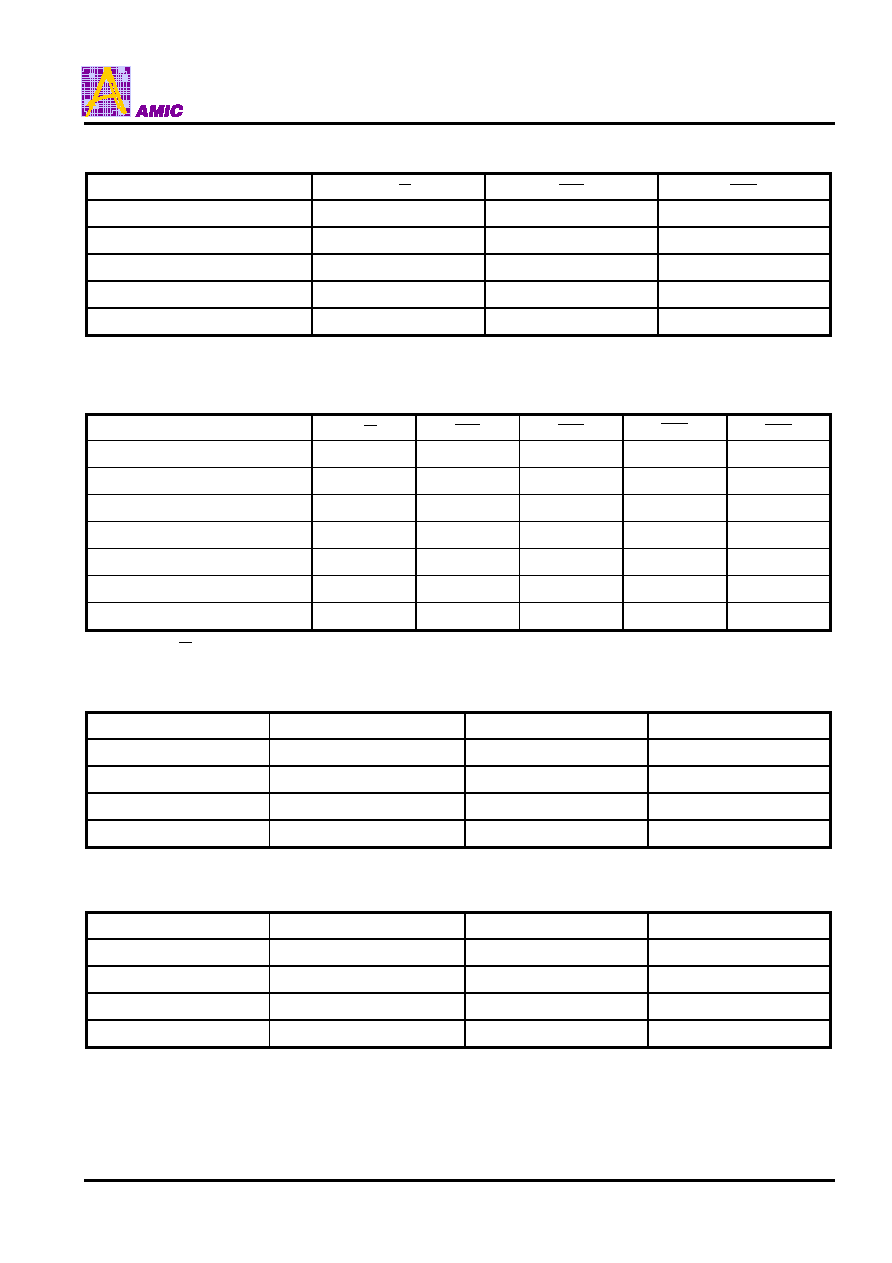
Revision History
Rev. No. History Issue
Date Remark
0.0
Initial issue
July 13, 2005
Preliminary
0.1
Modify DC specification to exact value
March 2, 2006

A67P8318/A67P7336
Preliminary
256K X 18, 128K X 36 LVTTL, Pipelined ZeBL
TM
SRAM
PRELIMINARY (March, 2006, Version 0.1)
1
AMIC Technology, Corp.
Features
Fast access time:
2.6/2.8/3.2/3.5/3.8/4.2 (250/227/200/166/150/133MHz)
Zero Bus Latency between READ and WRITE cycles
allows 100% bus utilization
Signal +2.5V
±
5% power supply
Individual Byte Write control capability
Clock enable (
CEN
) pin to enable clock and suspend
operations
Clock-controlled and registered address, data and
control signals
Registered output for pipelined applications
Three separate chip enables allow wide range of
options for CE control, address pipelining
Internally self-timed write cycle
Selectable BURST mode (Linear or Interleaved)
SLEEP mode (ZZ pin) provided
Available in 100 pin LQFP package
General Description
The AMIC Zero Bus Latency (ZeBL
TM
) SRAM family
employs high-speed, low-power CMOS designs using an
advanced CMOS process.
The A67P8318, A67P7336 SRAMs integrate a 256K X 18,
128K X 36 SRAM core with advanced synchronous
peripheral circuitry and a 2-bit burst counter. These SRAMs
are optimized for 100 percent bus utilization without the
insertion of any wait cycles during Write-Read alternation.
The positive edge triggered single clock input (CLK) controls
all synchronous inputs passing through the registers. The
synchronous inputs include all address, all data inputs,
active low chip enable (
CE
), two additional chip enables for
easy depth expansion (CE2,
CE2
), cycle start input
(ADV/ LD ), synchronous clock enable (
CEN
), byte write
enables (
BW1
,
BW2
,
BW3
,
BW4
) and read/write (R/
W
).
Asynchronous inputs include the output enable (
OE
), clock
(CLK), SLEEP mode (ZZ, tied LOW if unused) and burst
mode (MODE). Burst Mode can provide either interleaved or
linear operation, burst operation can be initiated by
synchronous address Advance/Load (ADV/LD ) pin in Low
state. Subsequent burst address can be internally
generated by the chip and controlled by the same input pin
ADV/LD in High state.
Write cycles are internally self-time and synchronous with
the rising edge of the clock input and when R/
W
is Low.
The feature simplified the write interface. Individual Byte
enables allow individual bytes to be written.
BW1
controls
I/Oa pins;
BW2
controls I/Ob pins;
BW3
controls I/Oc pins;
and
BW4
controls I/Od pins. Cycle types can only be
defined when an address is loaded.
The SRAM operates from a +2.5V power supply, and all
inputs and outputs are LVTTL-compatible. The device is
ideally suited for high bandwidth utilization systems.
A67P8318/A67P7336
PRELIMINARY (March, 2006, Version 0.1)
2
AMIC Technology, Corp.
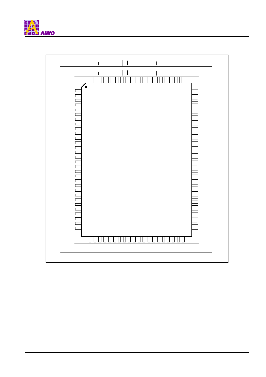
Pin Configuration
1
2
3
4
5
6
7
8
9
10
11
12
13
14
15
16
17
18
19
20
21
22
23
24
25
26
28
30
27
29
80
79
78
77
76
75
74
72
73
71
70
69
68
67
66
65
64
63
62
61
60
59
58
57
56
55
54
53
52
51
50
49
48
47
46
45
44
43
42
40
41
39
38
37
36
35
34
33
32
31
A1
7
A1
6
A1
5
A1
4
A1
3
A1
2
A1
1
NC
VC
C
VS
S
NC
NC
A0
A1
A2
A3
A4
A5
MO
D
E
81
82
83
84
85
86
87
88
89
90
91
92
93
94
95
96
97
98
99
100
256Kx18
A1
6
A1
5
A1
4
A1
3
A1
2
A1
1
A1
0
VC
C
VS
S
NC
A0
A1
A2
A3
A4
A5
MO
D
E
128Kx36
I/Ob
8
I/Oa
8
NC
NC
A6
A7
CE
2
NC
NC
VC
C
VS
S
CL
K
NC
NC
A8
A9
A10
NC
NC
VCCQ
VSSQ
NC
VSSQ
VCCQ
VSS
VCC
VCC
ZZ
VCCQ
VSSQ
NC
NC
VSSQ
VCCQ
NC
NC
NC
I/Oa
0
I/Oa
1
NC
NC
NC
VCCQ
VSSQ
NC
NC
VSSQ
VCCQ
VCC
VCC
VSS
VCCQ
VSSQ
NC
VSSQ
VCCQ
NC
NC
NC
I/Ob
8
I/Ob
7
I/Ob
6
VCC
I/Ob
4
CE
2
A7
A6
CL
K
VS
S
VC
C
A9
A8
NC
NC
VCCQ
VSSQ
VSSQ
VCCQ
VSS
VCC
VCC
ZZ
VCCQ
VSSQ
VSSQ
VCCQ
I/Ob
7
CE
CE
BW
4
BW
3
BW
2
BW2
BW
1
BW1
CE
2
CE
2
CE
N
CE
N
OE
OE
AD
V/
LD
AD
V/
LD
A67P8318E
A67P7336E
R/
W
R/
W
I/Ob
5
I/Ob
3
I/Ob
2
I/Ob
1
I/Ob
0
VCCQ
VSSQ
VSSQ
VCCQ
VCC
VCC
VSS
VCCQ
VSSQ
VSSQ
VCCQ
VCC
I/Oc
8
I/Oc
0
I/Oc
1
I/Oc
2
I/Oc
3
I/Oc
4
I/Oc
5
I/Oc
6
I/Oc
7
I/Od
0
I/Od
1
I/Od
2
I/Od
3
I/Od
4
I/Od
5
I/Od
6
I/Od
7
I/Od
8
I/Oa
2
I/Oa
3
I/Oa
4
I/Oa
5
I/Oa
6
I/Oa
7
I/Oa
8
I/Ob
6
I/Ob
5
I/Ob
4
I/Ob
3
I/Ob
2
I/Ob
1
I/Ob
0
I/Oa
7
I/Oa
6
I/Oa
5
I/Oa
4
I/Oa
3
I/Oa
2
I/Oa
1
I/Oa
0
NC
NC
A67P8318/A67P7336
PRELIMINARY (March, 2006, Version 0.1)
3
AMIC Technology, Corp.
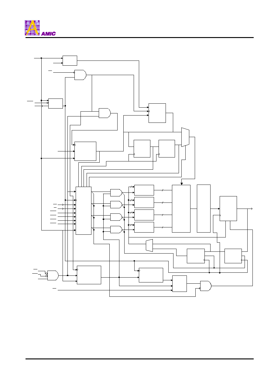
Block Diagram (128K X 36)
128Kx9x4
MEMORY
ARRAY
MODE
LOGIC
CLK
LOGIC
ADDRESS
REGISTERS
BURST
LOGIC
ADDRESS
COUNTER
CLR
WRITE
REGISTRY
&
CONTROL
LOGIC
BYTEa
WRITE
DRIVER
BYTEb
WRITE
DRIVER
BYTEc
WRITE
DRIVER
BYTEd
WRITE
DRIVER
9
9
9
9
9
9
9
9
OUTPUT
REGISTERS
&
OUTPUT
BUFFERS
DATA-IN
REGISTERS
CHIP
ENABLE
LOGIC
PIPELINED
ENABLE
LOGIC
OUTPUT
ENABLE
LOGIC
ZZ
MODE
ADV/LD
CLK
A0-A16
R/W
BW1
BW2
BW3
BW4
CE
CE2
CE2
OE
CEN
WRITE
ADDRESS
REGISTER
WRITE
ADDRESS
REGISTER
ADV/LD
DATA-IN
REGISTERS
I/O
s
SENSE
AMPS
A67P8318/A67P7336
PRELIMINARY (March, 2006, Version 0.1)
4
AMIC Technology, Corp.
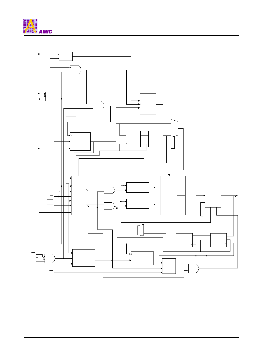
Block Diagram (256K X 18)
DATA-IN
REGISTERS
MODE
LOGIC
CLK
LOGIC
ADDRESS
REGISTERS
BURST
LOGIC
ADDRESS
COUNTER
CLR
WRITE
REGISTRY
&
CONTROL
LOGIC
BYTEa
WRITE
DRIVER
BYTEb
WRITE
DRIVER
9
9
256KX9X2
MEMORY
ARRAY
9
9
OUTPUT
REGISTERS
&
OUTPUT
BUFFERS
CHIP
ENABLE
LOGIC
PIPELINED
ENABLE
LOGIC
OUTPUT
ENABLE
LOGIC
ZZ
MODE
ADV/LD
CLK
A0-A17
R/W
BW1
BW2
CE
CE2
CE2
OE
CEN
WRITE
ADDRESS
REGISTER
WRITE
ADDRESS
REGISTER
ADV/LD
I/O
S
SENSE
AMPS
DATA-IN
REGISTERS
A67P8318/A67P7336
PRELIMINARY (March, 2006, Version 0.1)
5
AMIC Technology, Corp.
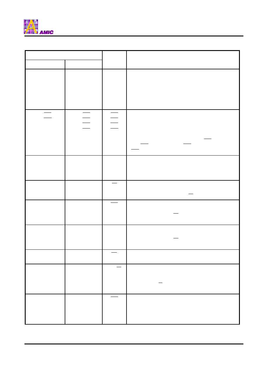
Pin Description
Pin No.
Symbol
Description
LQFP (X18)
LQFP (X36)
37
36
35, 34, 33, 32,
100, 99, 82, 81,
44, 45, 46, 47,
48, 49, 50
83
37
36
35, 34, 33, 32,
100, 99, 82, 81,
45, 46, 47, 48,
49, 50
44
A0
A1
A2 - A9
A11 - A17
A10
Synchronous Address Inputs : These inputs are registered
and must meet the setup and hold times around the rising
edge of CLK. A0 and A1 are the two lest significant bits
(LSB) of the address field and set the internal burst counter if
burst is desired.
93 (
BW1
)
94 (
BW2
)
93 (
BW1
)
94 (
BW2
)
95 (
BW3
)
96 (
BW4
)
BW1
BW2
BW3
BW4
Synchronous Byte Write Enables : These active low inputs
allow individual bytes to be written when a WRITE cycle is
active and must meet the setup and hold times around the
rising edge of CLK. BYTE WRITEs need to be asserted on
the same cycle as the address, BWs are associated with
addresses and apply to subsequent data.
BW1
controls I/Oa
pins;
BW2
controls I/Ob pins;
BW3
controls I/Oc pins;
BW4
controls I/Od pins.
89 89
CLK
Clock: This signal registers the address, data, chip enables,
byte write enables and burst control inputs on its rising edge.
All synchronous inputs must meet setup and hold times
around the clock are rising edge.
98 98
CE
Synchronous Chip Enable : This active low input is used to
enable the device. This input is sampled only when a new
external address is loaded (ADV/LD LOW).
92 92
CE2
Synchronous Chip Enable : This active low input is used to
enable the device and is sampled only when a new external
address is loaded (ADV/LD LOW). This input can be used
for memory depth expansion.
97
97
CE2
Synchronous Chip Enable : This active high input is used to
enable the device and is sampled only when a new external
address is loaded (ADV/LD LOW). This input can be used
for memory depth expansion.
86 86
OE
Output Enable : This active low asynchronous input enables
the data I/O output drivers.
85 85
ADV/LD
Synchronous Address Advance/Load : When HIGH, this
input is used to advance the internal burst counter,
controlling burst access after the external address is loaded.
When HIGH, R/
W
is ignored. A LOW on this pin permits a
new address to be loaded at CLK rising edge.
87 87
CEN
Synchronous Clock Enable : This active low input permits
CLK to propagate throughout the device. When HIGH, the
device ignores the CLK input and effectively internally
extends the previous CLK cycle. This input must meet setup
and hold times around the rising edge of CLK.

A67P8318/A67P7336
PRELIMINARY (March, 2006, Version 0.1)
6
AMIC Technology, Corp.
Pin Description (continued)
Pin No.
Symbol
Description
LQFP (X18)
LQFP (X36)
64
64
ZZ
Snooze Enable : This active high asynchronous input causes
the device to enter a low-power standby mode in which all
data in the memory array is retained. When active, all other
inputs are ignored.
88 88
R/
W
Read/Write : This active input determines the cycle type
when ADV/LD is LOW. This is the only means for
determining READs and WRITEs. READ cycles may not be
converted into WRITEs (and vice versa) other than by
loading a new address. A LOW on this pin permits BYTE
WRITE operations and must meet the setup and hold times
around the rising edge of CLK. Full bus width WRITEs occur
if all byte write enables are LOW.
74, 73, 72, 69, 68,
63, 62, 59, 58,
24, 23, 22, 19, 18
13, 12, 9, 8
51, 52, 53, 56, 57,
58, 59, 62, 63
68, 69, 72, 73, 74,
75, 78, 79, 80
1, 2, 3, 6, 7, 8, 9,
12, 13,
18, 19, 22, 23, 24,
25, 28, 29, 30
I/Oa
I/Ob
I/Oc
I/Od
SRAM Data I/O : Byte "a" is I/Oa pins; Byte "b" is I/Ob pins;
Byte "c" is I/Oc pins; Byte "d" is I/Od pins. Input data must
meet setup and hold times around CLK rising edge.
31 31
MODE
Mode : This input selects the burst sequence. A LOW on this
pin selects linear burst. NC or HIGH on this pin selects
interleaved burst. Do not alter input state while device is
operating.
1, 2, 3, 6, 7, 25, 28,
29, 30, 38, 39,
42,43 51, 52, 53,
56, 57, 75, 78, 79,
95, 96
38,39,42,43
NC
No Connect : These pins can be left floating or connected to
GND to minimize thermal impedance.
15, 41, 65, 91
15, 41, 65, 91
VCC
Power Supply : See DC Electrical Characteristics and
Operating Conditions for range.
14, 16, 66
14, 16, 66
VCC
These pins do not have to be connected directly to VCC as
long as the input voltage is
V
IH
. This input is not connected
to VCC bus internally.
4, 11, 20, 27,
54, 61, 70, 77
4, 11, 20, 27, 54,
61, 70, 77
VCCQ
Isolated Output Buffer Supply : See DC Electrical
Characteristics and Operating Conditions for range.
17, 40, 90
17, 40, 90
VSS
Ground : GND.
5,10,21,26,
55,60,71,76
5,10,21,26,
55,60,71,76
VSSQ
Isolated Output Buffer Ground

A67P8318/A67P7336
PRELIMINARY (March, 2006, Version 0.1)
7
AMIC Technology, Corp.
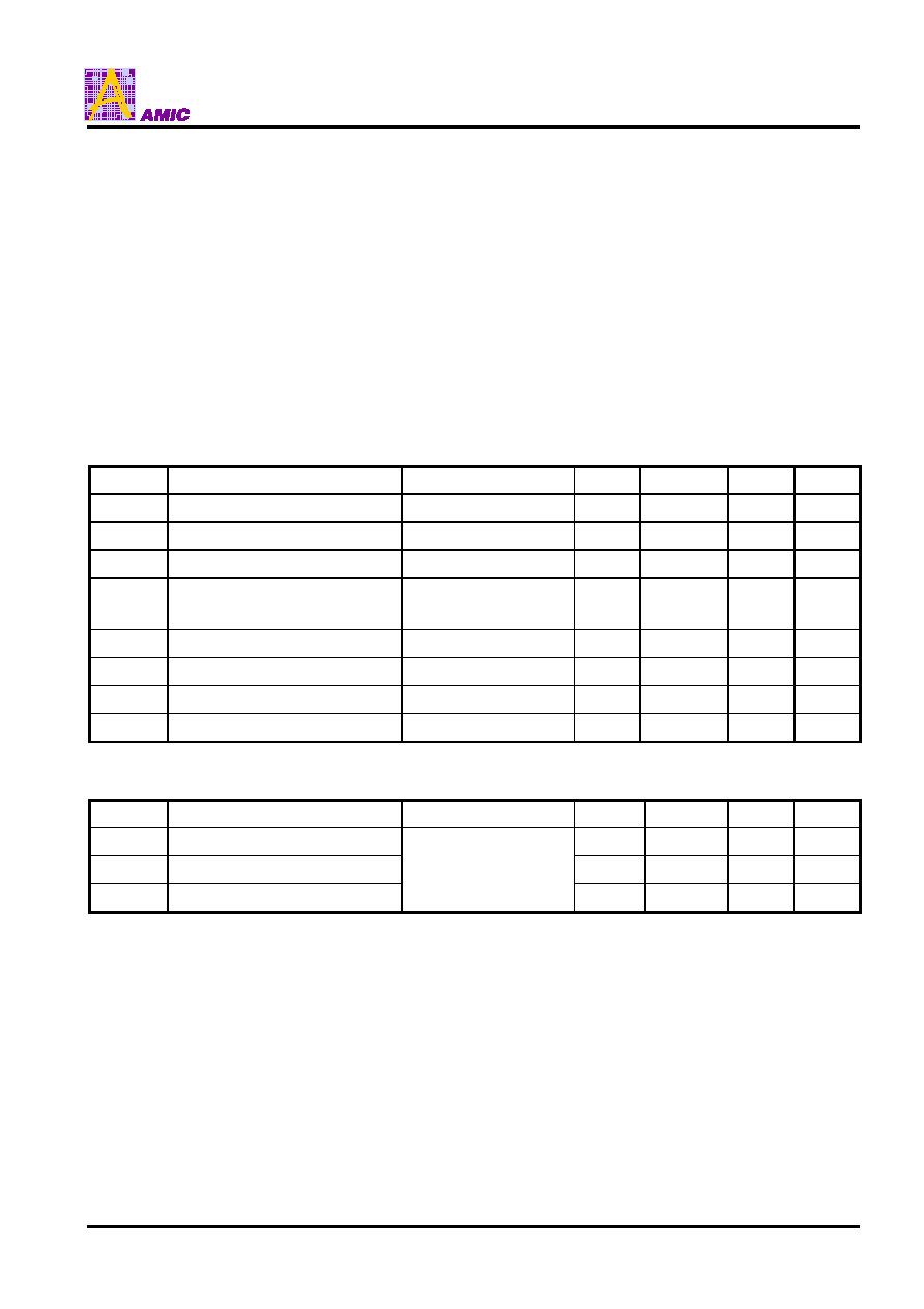
Truth Table (Notes 5 - 7)
Operation
Address
Used
CE
CE2
CE2
ZZ
ADV/
LD
R/
W
BWx
OE
CEN
CLK I/O Notes
Deselected Cycle,
Power-down
None H
X X L L X X X L L
H High-Z
Deselected Cycle,
Power-down
None X
H X L L X X X L L
H High-Z
Deselected Cycle,
Power-down
None X
X L L L X X X L L
H High-Z
Continue Deselect
Cycle
None X
X X L H X X X L L
H High-Z
1
READ Cycle
(Begin Burst)
External L L H L L H X L L L
H Q
READ Cycle
(Continue Burst)
Next X
X X L H X X L L
L
H Q 1,7
NOP/Dummy READ
(Begin Burst)
External L L H L L H X H L L
H High-Z
2
Dummy READ
(Continue Burst)
Next X
X X L H X X H L
L
H High-Z
1,2,7
WRITE Cycle
(Begin Burst)
External
L
L H L L L L X L
L
H D
3
WRITE Cycle
(Continue Burst)
Next X
X X L H X L X L
L
H D 1,3,7
NOP/WRITE Abort
(Begin Burst)
None L L H L L L H X L
L
H High-Z
2,3
WRITE Abort
(Continue Burst)
Next X
X X L H X H X L
L
H High-Z
1,2,3,7
IGNORE Clock Edge
(Stall)
Current X X X L X X X X H L
H -
4
SLEEP Mode
None
X
X
X
H
X
X
X
X
X
X
High-Z
Notes:
1. Continue Burst cycles, whether READ or WRITE, use the same control inputs. The type of cycle performed (READ or
WRITE) is chosen in the initial Begin Burst cycle. A Continue Deselect cycle can only be entered if a Deselect cycle is
executed first.
2. Dummy READ and WRITE Abort cycles can be considered NOPs because the device performs no operation. A WRITE
Abort means a WRITE command is given, but no operation is performed.
3. OE may be wired LOW to minimize the number of control signals to the SRAM. The device will automatically turn off the
output drivers during a WRITE cycle. Some users may use OE when the bus turn-on and turn-off times do not meet their
requirements.
4. If an Ignore Clock Edge command occurs during a READ operation, the I/O bus will remain active (Low-Z). If it occurs
during a WRITE cycle, the bus will remain in High-Z. No WRITE operations will be performed during the Ignored Clock
Edge cycle.
5. X means "Don't Care." H means logic HIGH. L means logic LOW.
BWx
= H means all byte write signals (
BW1
,
BW2
,
BW3
and
BW4
) are HIGH.
BWx
= L means one or more byte write signals are LOW.
6.
BW1
enables WRITEs to Byte "a" (I/Oa pins);
BW2
enables WRITEs to Byte "b" (I/Ob pins);
BW3
enables WRITEs to
Byte "c" (I/Oc pins);
BW4
enables WRITEs to Byte "d" (I/Od pins).
7. The address counter is incremented for all Continue Burst cycles.
A67P8318/A67P7336
PRELIMINARY (March, 2006, Version 0.1)
8
AMIC Technology, Corp.
Partial Truth Table for READ/WRITE Commands (X18)
Operation R/
W
BW1
BW2
READ H
X
X
WRITE Byte "a"
L
L
H
WRITE Byte "b"
L
H
L
WRITE all bytes
L
L
L
WRITE Abort/NOP
L
H
H
Note : Using and BYTE WRITE(s), any one or more bytes may be written.
Partial Truth Table for READ/WRITE Commands (X36)
Operation R/
W
BW1
BW2
BW3
BW4
READ
H X X X X
WRITE Byte "a"
L
L
H
H
H
WRITE Byte "b"
L
H
L
H
H
WRITE Byte "c"
L
H
H
L
H
WRITE Byte "d"
L
H
H
H
L
WRITE all bytes
L
L
L
L
L
WRITE
Abort/NOP
L H H H H
Note : Using R/
W
and BYTE WRITE(s), any one or more bytes may be written.
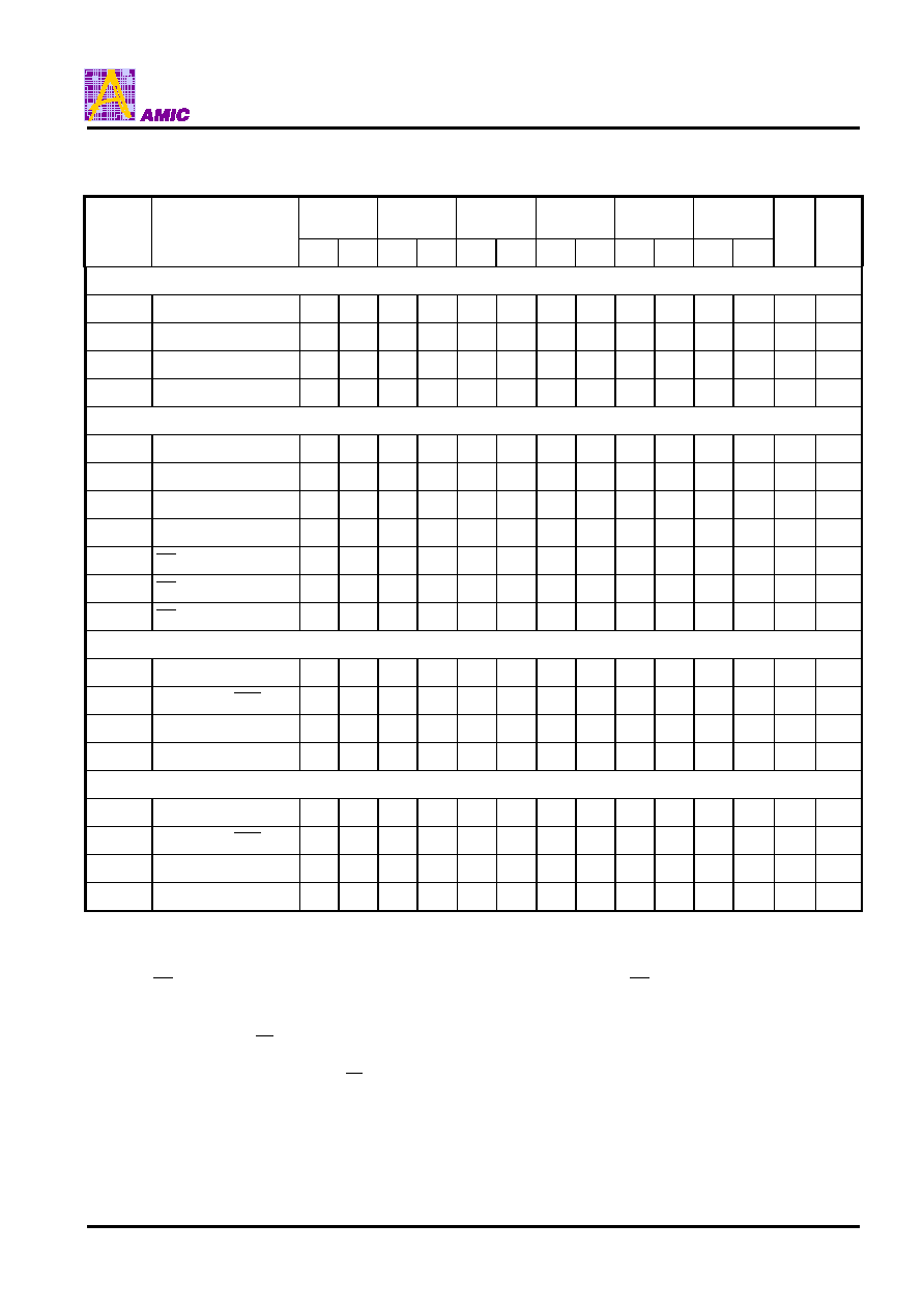
Linear Burst Address Table (MODE = LOW)
First Address (External) Second
Address
(Internal)
Third Address (Internal) Fourth
Address
(Internal)
X . . . X00
X . . . X01
X . . . X10
X . . . X11
X . . . X01
X . . . X10
X . . . X11
X . . . X00
X . . . X10
X . . . X11
X . . . X00
X . . . X01
X . . . X11
X . . . X00
X . . . X01
X . . . X10
Interleaved Burst Address Table (MODE = HIGH or NC)
First Address (External) Second
Address
(Internal)
Third Address (Internal) Fourth
Address
(Internal)
X . . . X00
X . . . X01
X . . . X10
X . . . X11
X . . . X01
X . . . X00
X . . . X11
X . . . X10
X . . . X10
X . . . X11
X . . . X00
X . . . X01
X . . . X11
X . . . X10
X . . . X01
X . . . X00
A67P8318/A67P7336
PRELIMINARY (March, 2006, Version 0.1)
9
AMIC Technology, Corp.
Absolute Maximum Ratings*
Power Supply Voltage (VCC) . . . . . . . . . . -0.3V to +3.6V
Voltage Relative to GND for any Pin Except VCC (Vin,
Vout) . . . . . . . . . . . . . . . . . . . . . . . . -0.3V to VCC +0.3V
Operating Temperature (Topr) . . . . . . . . . . . 0
°
C to 70
°
C
Storage Temperature (Tbias) . . . . . . . . . . -10
°
C to 85
°
C
Storage Temperature (Tstg) . . . . . . . . . . -55
°
C to 125
°
C
*Comments
Stresses above those listed under "Absolute Maximum
Ratings" may cause permanent damage to this device.
These are stress ratings only. Functional operation of
this device at these or any other conditions above those
indicated in the operational sections of this specification
is not implied or intended. Exposure to the absolute
maximum rating conditions for extended periods may
affect device reliability.
DC Electrical Characteristics and Operating Conditions
(0
°
C
T
A
70
°
C, VCC, VCCQ = +2.5V
±
5% unless otherwise noted)
Symbol Parameter
Conditions
Min.
Max.
Unit
Note
V
IH
Input High Voltage
1.7
VCC+0.3
V
1,2
V
IL
Input Low Voltage
-0.3
0.8
V
1,2
IL
I
Input Leakage Current
0V
V
IH
VCC
-2.0
2.0
µ
A
IL
O
Output Leakage Current
Output(s) disabled,
0V
V
IN
VCC
-2.0 2.0
µ
A
V
OH
Output High Voltage
I
OH
= -1.0mA
2.0
V
1,3
V
OL
Output Low Voltage
I
OL
= 1.0mA
0.4
V
1,3
VCC Supply
Voltage
2.375 2.625
V
1
VCCQ
Isolated Output Buffer Supply
2.375
VCC
V
1,4
Capacitance
Symbol Parameter
Conditions
Typ.
Max.
Unit
Note
C
I
Control Input Capacitance
3
4
pF
6
C
O
Input/Output Capacitance (I/O)
4
5
pF
6
C
A
Address
Capacitance
T
A
= 25
°
C; f = 1MHz
VCC = 2.5V
3 3.5 pF
6
Note : 1. All voltages referenced to VSS (GND).
2. Overshoot : V
IH
+4.6V for t
t
KHKH
/2 for I
20mA
Undershoot : V
IL
-0.7V for t
t
KHKH
/2 for I
20mA
Power-up :
V
IH
+2.625V and VCC
2.625V for t
200ms
3. The load used for V
OH
, V
OL
testing is shown in Figure 2. AC load current is higher than the shown DC values.
AC I/O curves are available upon request.
4. VCC and VCCQ can be externally wired together to the same power supply.
5. This parameter is sampled.

A67P8318/A67P7336
PRELIMINARY (March, 2006, Version 0.1)
10
AMIC Technology, Corp.
I
CC
Operating Condition and Maximum Limits
Max.
Symbol Parameter
-2.6 -2.8
-3.2
-3.5
-3.8
-4.2
Unit
Conditions
I
CC
Power Supply
Current : Operating
230 200
185
170
160
145
mA
Device selected; All inputs
V
IL
or
V
IH
; Cycle time
t
KC
(MIN);
VCC = MAX; Outputs open
I
SB
Standby
30 30 30 30 30 30 mA
Device deselected; VCC = MAX;
All inputs
VSS+0.2 or
VCC-
0.2; Cycle time
t
KC
(MIN)
I
SB1
Standby
30 30 30 30 30 30 mA
Device deselected; VCC = MAX;
All inputs
V
IL
; or
V
IH
;
All inputs static;
CLK frequency=MAX
ZZ
VCC-0.2V
I
SB2
Standby
15 15 15 15 15 15 mA
Device deselected; VCC = MAX;
All inputs
VSS+0.2 or
VCC-
0.2; All inputs static; CLK
frequency=0
ZZ
0.2V
I
SB2Z
SLEEP
Mode
15 15 15 15 15 15 mA
ZZ
V
IH
A67P8318/A67P7336
PRELIMINARY (March, 2006, Version 0.1)
11
AMIC Technology, Corp.
AC Characteristics
(Note 4)
(0
°
C
T
A
70
°
C, VCC = +2.5V
±
5%)
-2.6 -2.8 -3.2 -3.5 -3.8 -4.2
Unit
Note
Symbol Parameter
Min Max Min
Max
Min
Max
Min
Max
Min
Max Min Max
Clock
t
KHKH
Clock
cycle
time
4.0 - 4.4
- 5.0
- 6.0
- 6.7
- 7.5 - ns
t
KF
Clock
frequency
- 250 - 227
- 200
- 166
- 150 - 133
MH
t
KHKL
Clock
HIGH
time
1.7 - 2.0
- 2.0
- 2.2
- 2.5
- 3.0 - ns
t
KLKH
Clock
LOW
time
1.7 - 2.0
- 2.0
- 2.2
- 2.5
- 3.0 - ns
Output Times
t
KHQV
Clock to output valid
-
2.6
-
2.8
-
3.2
-
3.5
-
3.8
-
4.2
ns
t
KHQX
Clock to output invalid
1.5
-
1.5
-
1.5
-
1.5
-
1.5
-
1.5
-
ns
t
KHQX1
Clock to output in Low-Z
1.5
-
1.5
-
1.5
-
1.5
-
1.5
-
1.5
-
ns
1,2,3
t
KHQZ
Clock to output in High-Z
1.5
2.6
1.5
2.8
1.5
3.0
1.5
3.0
1.5
3.0
1.5
3.5
ns
1,2,3
t
GLQV
OE
to output valid
- 2.6 - 2.8
- 3.2
- 3.5
- 3.8 - 4.2 ns 4
t
GLQX
OE
to output in Low-Z
0 - 0 - 0 - 0 - 0 - 0 - ns
1,2,3
t
GHQZ
OE
to output in High-Z
- 2.6 - 2.8
- 3.0
- 3.0
- 3.0 - 3.5 ns 1,2,3
Setup Times
t
AVKH
Address
1.2 - 1.4
- 1.4
- 1.5
- 1.5
- 1.5 - ns 5
t
EVKH
Clock enable (
CEN
)
1.2 - 1.4
- 1.4
- 1.5
- 1.5
- 1.5 - ns 5
t
CVKH
Control
signals
1.2 - 1.4
- 1.4
- 1.5
- 1.5
- 1.5 - ns 5
t
DVKH
Data-in
1.2 - 1.4
- 1.4
- 1.5
- 1.5
- 1.5 - ns 5
Hold Times
t
KHAX
Address
0.3 - 0.4
- 0.4
- 0.5
- 0.5
- 0.5 - ns 5
t
KHEX
Clock enable (
CEN
)
0.3 - 0.4
- 0.4
- 0.5
- 0.5
- 0.5 - ns 5
t
KHCX
Control
signals
0.3 - 0.4
- 0.4
- 0.5
- 0.5
- 0.5 - ns 5
t
KHDX
Data-in
0.3 - 0.4
- 0.4
- 0.5
- 0.5
- 0.5 - ns 5
Notes: 1. This parameter is sampled.
2. Output loading is specified with C1=5pF as in Figure 2.
3. Transition is measured
±
200mV from steady state voltage.
4. OE can be considered a "Don't Care" during WRITE; however, controlling OE can help fine-tune a system for
turnaround timing.
5. This is a synchronous device. All addresses must meet the specified setup and hold times for all rising edges of
CLK when ADV/LD is LOW and chip enabled. All other synchronous inputs meet the setup and hold times with
stable logic levels for all rising edges of clock (CLK) when the chip is enabled. Chip enable must be valid at each
rising edge of CLK (when ADV/LD is LOW) to remain enabled.
A67P8318/A67P7336
PRELIMINARY (March, 2006, Version 0.1)
12
AMIC Technology, Corp.
AC Test Conditions
Input Pulse Levels
GND to 2.5V
Input Rise and Fall Times
1.0ns
Input Timing Reference Levels
1.25V
Output Reference Levels
1.25V
Output Load
See Figures 1 and 2
1538
Q
+2.5V
1667
5pF
Z
O
=50
Q
50
V
T
=1.25V
Figure 1
Output Load Equivalent
Figure 2
Output Load Equivalent
A67P8318/A67P7336
PRELIMINARY (March, 2006, Version 0.1)
13
AMIC Technology, Corp.
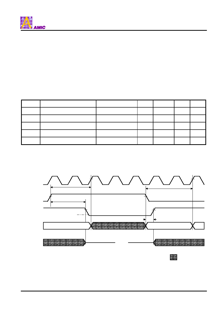
SLEEP Mode
SLEEP Mode is a low current "Power-down" mode in which
the device is deselected and current is reduced to I
SB2Z
. This
duration of SLEEP Mode is dictated by the length of time the
ZZ is in a HIGH state. After entering SLEEP Mode, all inputs
except ZZ become disabled and all outputs go to High-Z.
The ZZ pin is asynchronous, active high input that causes the
device to enter SLEEP Mode. When the ZZ pin becomes
logic HIGH, ISB2Z is guaranteed after the time t
ZZI
is met.
Any operation pending when entering SLEEP Mode is not
guaranteed to successfully complete. Therefore, SLEEP
Mode (READ or WRITE) must not be initiated until valid
pending operations are completed. Similarly, when exiting
SLEEP Mode during t
RZZ
, only a DESELECT or READ cycle
should be given while the SRAM is transitioning out of
SLEEP Mode.
SLEEP Mode Electrical Characteristics
(VCC, VCCQ = +2.5V
±
5%)
Symbol Parameter
Conditions
Min.
Max.
Unit
Note
I
SB2Z
Current during SLEEP Mode
ZZ
V
IH
-
15
mA
t
ZZ
ZZ active to input ignored
0
2(t
KHKH
) ns 1
t
RZZ
ZZ inactive to input sampled
0
2(t
KHKH
) ns 1
t
ZZI
ZZ active to snooze current
- 2(t
KHKH
) ns 1
t
RZZI
ZZ inactive to exit snooze current
0
ns
1
Note : 1. This parameter is sampled.
SLEEP Mode Waveform
t
RZZ
t
ZZ
t
ZZI
I
ISB2Z
High-Z
DESELECT or READ Only
Output
(Q)
ALL INPUTS
(except ZZ)
I
SUPPLY
ZZ
CLK
: Don't Care
t
RZZI
A67P8318/A67P7336
PRELIMINARY (March, 2006, Version 0.1)
14
AMIC Technology, Corp.
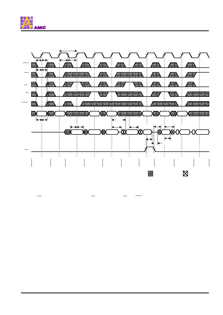
READ/WRITE Timing
Note :
1. For this waveform, ZZ is tied LOW.
2. Burst sequence order is determined by MODE (0 = linear, 1 = interleaved). BRST operations are optional.
3.
CE
represents three signals. When
CE
= 0, it represents
CE
= 0,
CE2
= 0, CE2 = 1.
4. Data coherency is provided for all possible operations. If a READ is initiated the most current data is used. The
most recent data may be from the input data register.
A3
A2
A1
A4
A5
D(A1)
WRITE
D(A1)
WRITE
D(A2)
BURST
WRITE
D(A2+1)
READ
Q(A3)
READ
Q(A4)
BURST
READ
Q(A4+1)
WRITE
D(A5)
READ
Q(A6)
WRITE
D(A7)
DESELECT
: Don't Care
: Undefined
1
2
3
4
5
t
GLQX
t
KHKH
6
7
8
9
10
CLK
CEN
CE
ADV/
LD
R/W
BWx
ADDRESS
I/O
COMMAND
A6
A7
D(A2)
D(A2+1)
Q(A6)
D(A5)
Q(A4+1)
Q(A4)
Q(A3)
OE
t
KLKH
t
EVKH
t
KHEX
t
KHKL
t
KHCX
t
CVKH
t
KHAX
t
AVKH
t
KHDX
t
DVKH
t
KHQZ
t
GLQV
t
KHQX
t
GHQZ
t
KHQX
t
KHQV
t
KHQX1
A67P8318/A67P7336
PRELIMINARY (March, 2006, Version 0.1)
15
AMIC Technology, Corp.
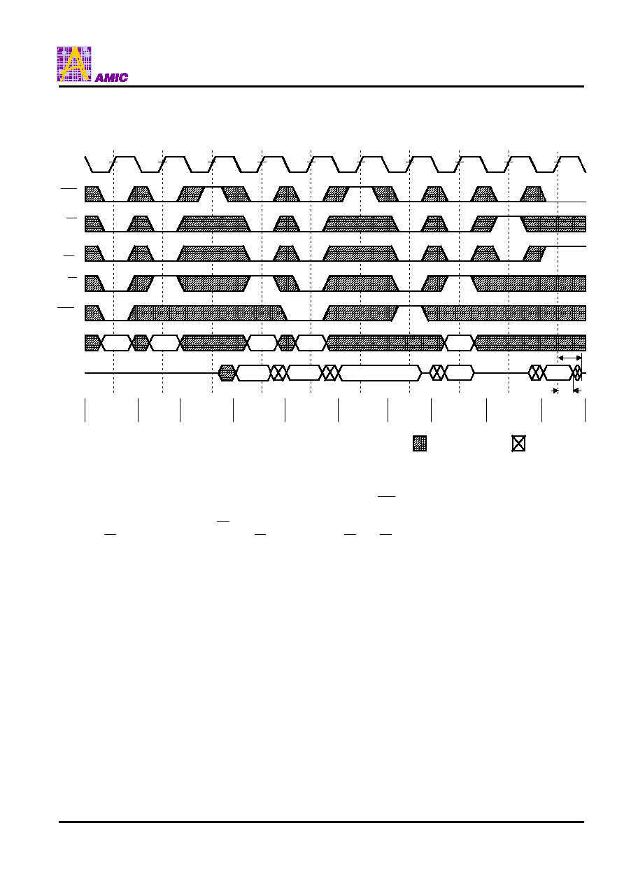
NOP, STALL and Deselect Cycles
Note :
1. The IGNORE CLOCK EDGE or STALL cycle (clock 3) illustrates
CEN
being used to create a "pause." A WRITE is
not performed during this cycle.
2. For this waveform, ZZ and
OE
are tied LOW.
3.
CE
represents three signals. When
CE
= 0, it represents
CE
= 0,
2
CE
= 0, CE2 = 1.
4. Data coherency is provided for all possible operations. If a READ is initiated, the most current data is used. The
most recent data may be from the input data register.
A3
A2
A1
A4
A5
Q(A5)
D(A4)
Q(A3)
Q(A2)
D(A1)
WRITE
D(A1)
READ
Q(A2)
STALL
READ
Q(A3)
WRITE
D(A4)
STALL
NOP
READ
Q(A5)
DESELECT
CONTINUE
DESELECT
: Don't Care
: Undefined
1
2
3
4
5
t
KHQX
t
KHQZ
6
7
8
9
10
CLK
CEN
CE
ADV/
LD
R/W
BWx
ADDRESS
I/O
COMMAND

A67P8318/A67P7336
PRELIMINARY (March, 2006, Version 0.1)
16
AMIC Technology, Corp.
Ordering Information
Part No.
Configure
Cycle Time / Access Time
Package
A67P8318E-4.2
7.5ns / 4.2ns
100L LQFP
A67P8318E-4.2F
7.5ns / 4.2ns
100L Pb-Free LQFP
A67P8318E-3.8
6.7ns / 3.8ns
100L LQFP
A67P8318E-3.8F
6.7ns / 3.8ns
100L Pb-Free LQFP
A67P8318E-3.5
6.0ns / 3.5ns
100L LQFP
A67P8318E-3.5F
6.0ns / 3.5ns
100L Pb-Free LQFP
A67P8318E-3.2
5.0ns / 3.2ns
100L LQFP
A67P8318E-3.2F
5.0ns / 3.2ns
100L Pb-Free LQFP
A67P8318E-2.8
4.4ns / 2.8ns
100L LQFP
A67P8318E-2.8F
4.4ns / 2.8ns
100L Pb-Free LQFP
A67P8318E-2.6
4.0ns / 2.6ns
100L LQFP
A67P8318E-2.6F
256K X 18
4.0ns / 2.6ns
100L Pb-Free LQFP
A67P7336E-4.2
7.5ns / 4.2ns
100L LQFP
A67P7336E-4.2F
7.5ns / 4.2ns
100L Pb-Free LQFP
A67P7336E-3.8
6.7ns / 3.8ns
100L LQFP
A67P7336E-3.8F
6.7ns / 3.8ns
100L Pb-Free LQFP
A67P7336E-3.5
6.0ns / 3.5ns
100L LQFP
A67P7336E-3.5F
6.0ns / 3.5ns
100L Pb-Free LQFP
A67P7336E-3.2
5.0ns / 3.2ns
100L LQFP
A67P7336E-3.2F
5.0ns / 3.2ns
100L Pb-Free LQFP
A67P7336E-2.8
4.4ns / 2.8ns
100L LQFP
A67P7336E-2.8F
4.4ns / 2.8ns
100L Pb-Free LQFP
A67P7336E-2.6
4.0ns / 2.6ns
100L LQFP
A67P7336E-2.6F
128K X 36
4.0ns / 2.6ns
100L Pb-Free LQFP
A67P8318/A67P7336
PRELIMINARY (March, 2006, Version 0.1)
17
AMIC Technology, Corp.
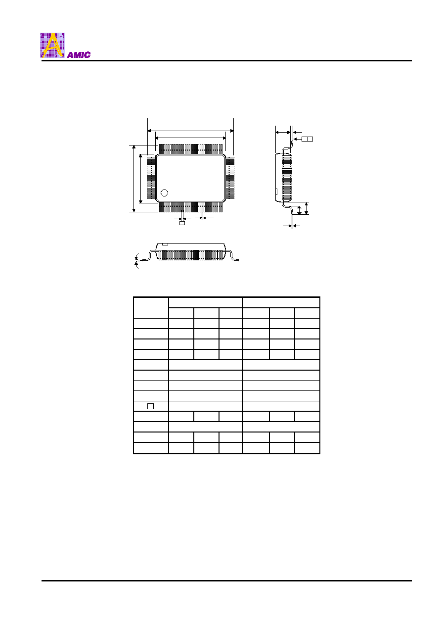
Package Information
LQFP 100L Outline Dimensions
unit: inches/mm
Symbol
Dimensions in inches
Dimensions in mm
Min.
Nom.
Max.
Min.
Nom.
Max.
A
1
0.002
-
0.006
0.05 - 0.15
A
2
0.053
0.055
0.057
1.35
1.40
1.45
b 0.009
0.012
0.015
0.22
0.30
0.38
c 0.004
-
0.008
0.09 - 0.20
H
E
0.866 BSC
22.00 BSC
E
0.787 BSC
20.00 BSC
H
D
0.630 BSC
16.00 BSC
D
0.551 BSC
14.00 BSC
e
0.026 BSC
0.65 BSC
L 0.018
0.024
0.030
0.45
0.60
0.75
L
1
0.039 REF
1.00 REF
y -
-
0.004
-
-
0.10
0
°
3.5
°
7
°
0
°
3.5
°
7
°
Notes:
1. Dimensions D and E do not include mold protrusion.
2. Dimensions b does not include dambar protrusion.
Total in excess of the b dimension at maximum material condition.
Dambar cannot be located on the lower radius of the foot.
31
50
51
80
81
100
H
D
D
E
H
E
1
30
b
D y
A
1
A
2
L
1
c
e
L