Microsoft Word - A7101_040510.doc

A7101
Preliminary
2.4GHz FSK Transceiver
PRELIMINARY (March 2004, Version 0.4)
AMIC Technology, Corp.
Document Title
2.4GHz FSK Transceiver
Revision History
Rev. No. History Issue
Date Remark
0.0
Initial issue
August 2, 2002
Preliminary
0.1 Modify
current
consumption, Tx output power, sensitivity,
October 16, 2002
Preliminary
RSSI range, frequency deviation, data rate, SPI interface,
and pin description.
0.2
Modify X'TAL Settling Time, Tx output power (Hi power)
June 9, 2003
Preliminary
Application Circuit, and delete X'TAL accuracy
0.3
Modify Tx output power (Hi power)
Dec. 30 2003
Preliminary
0.4
Modify data rate and calibration mode
March 10, 2004
Preliminary
Important Notice:
AMIC reserves the right to make changes to its products or to discontinue any integrated circuit product or
service without notice. AMIC integrated circuit products are not designed, intended, authorized, or warranted to
be suitable for use in life-support applications, devices or systems or other critical applications. Use of AMIC
products in such applications is understood to be fully at the risk of the customer.
A7101
Preliminary
2.4GHz FSK Transceiver
PRELIMINARY (March 2004, Version 0.4)
1
AMIC Technology, Corp.
Typical Applications
Wireless Mouse and Keyboard
2.4GHz ISM Band Communication System
Two way wireless Transceiver
Wireless toy
Wireless Modem
General Description
The A7101 is a monolithic CMOS integrated circuit
intended for use as a low cost FSK transceiver in wireless
applications. The device is provided in 48-lead plastic
QFN7X7 packaging and is designed to function as a
complete FSK transceiver. It is intended for wireless
applications in the 2.4GHz to 2.5GHz ISM band. This chip
features a fully programmable frequency synthesizer with
integrated VCO circuitry.
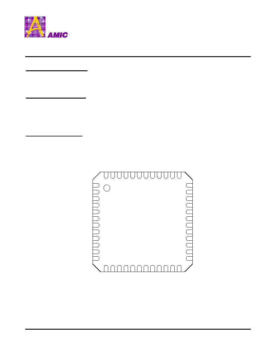
Pin Configurations
1
2
3
4
5
6
7
8
13
14
15
16
17
18
19
20
36
35
34
33
32
31
30
29
48
47
46
45
44
43
42
41
VDD_A
RXDATA
BR_RX
NC
RFIO
BP_BUF
TXDATAIN
XTAL1
LIM2INP
LIM1OUT
LIM1INN
LIM1INP
MIXOUT
VDD_VCO
BP_VCO
LIM2INN
LV
O
U
T
LV
I
N
VDD_D
VUOT
SPI_
D
ATA
S
P
I
_CLO
CK
SPI_
L
A
TCH
M
O
DSEL
0
CM
PVIP
EN_
A
FC
CAP2
_
A
FC
CAP1
_
A
FC
CAP3
_
A
FC
LP
FO
UT
LP
FI
NN
LP
FI
NP
A7101
9
XTAL2
10
XTALOUT
11
CAPSW
12
BP_REG
21
REGFB
22
EN_
R
EG
23
VIN
24
M
O
DSEL
1
28
VT
27
BR_VCO
26
CHPOUT
25
LD
40
TA
NK
1
39
TA
NK
2
3
8
RSSI
37
MUTE
Figure 1. QFN Package Top View
A7101
PRELIMINARY (March 2004, Version 0.4)
2
AMIC Technology, Corp.
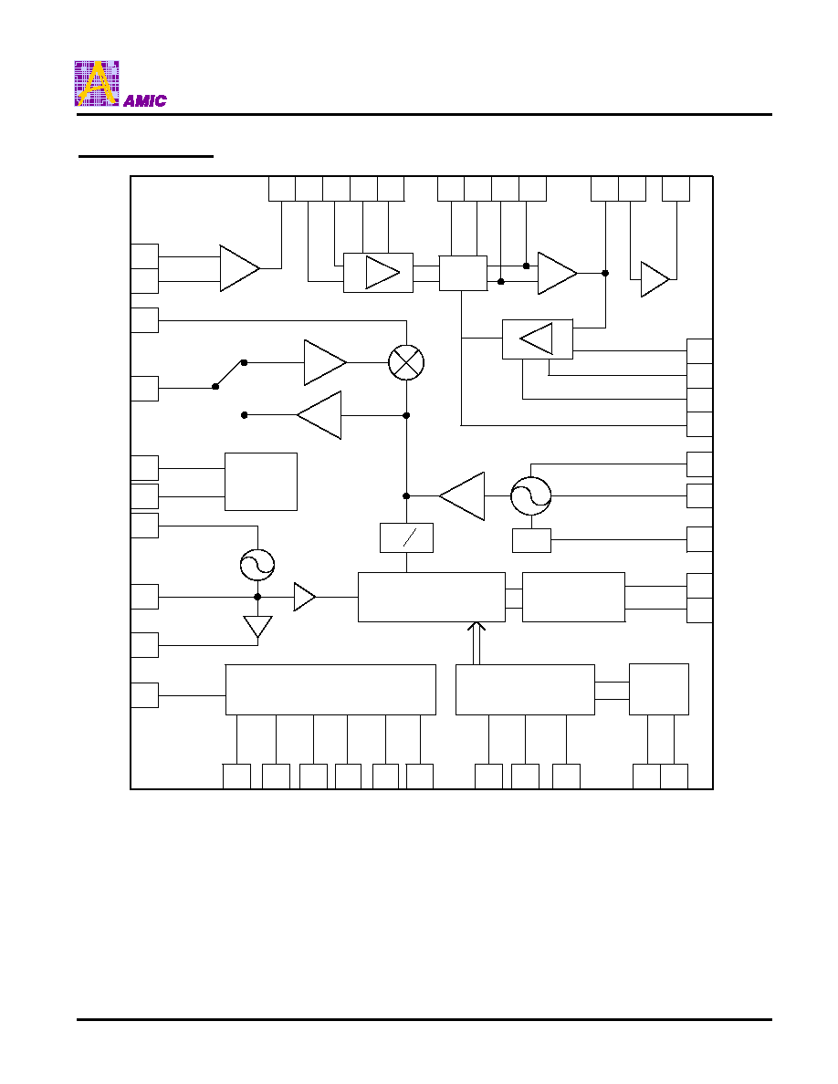
Block Diagram
REGFB
SPI_C
LOC
K
M
O
D
SEL0
M
O
D
SEL1
VT
SPI_LATC
H
SPI_D
ATA
BP_R
E
G
LVOU
T
LVIN
VOU
T
EN
_R
EG
VIN
16
XTAL2
XTALOUT
TXDATAIN
XTAL1
Phase Detector
Charge Pump
LPFOU
T
LNA
RFIO
CAPSW
FSK
Modulation
Circuit
CHPOUT
LD
BR_VCO
BP_VCO
EN_AFC
CAP2_AFC
CAP1_AFC
CAP3_AFC
LIM
1
OU
T
LIM1INN
LIM1INP
MIXOUT
Integrator
Limiter2
Limiter1
MUTE
R
SSI
LIM
2
IN
N
LIM
2
IN
P
LPFIN
N
LPFIN
P
TANK1
TANK2
RX
DA
TA
C
M
PVIP
Data Slicer
OSC
VCO
Voltage Regulator &
Low voltage detector
34 35 36 37 38
39 40 41 42
43 48
2
46
45
44
29
28
27
26
25
24
20
19
18
17
23
14
13
12
21
10
9
8
11
7
5
31
32
33
DEMOD
Mode
Selection
SPI
22
Buffer
Bias
PA
Counter
33
32
�
LPF
47
Figure 2. System Block Diagram
A7101
PRELIMINARY (March 2004, Version 0.4)
3
AMIC Technology, Corp.
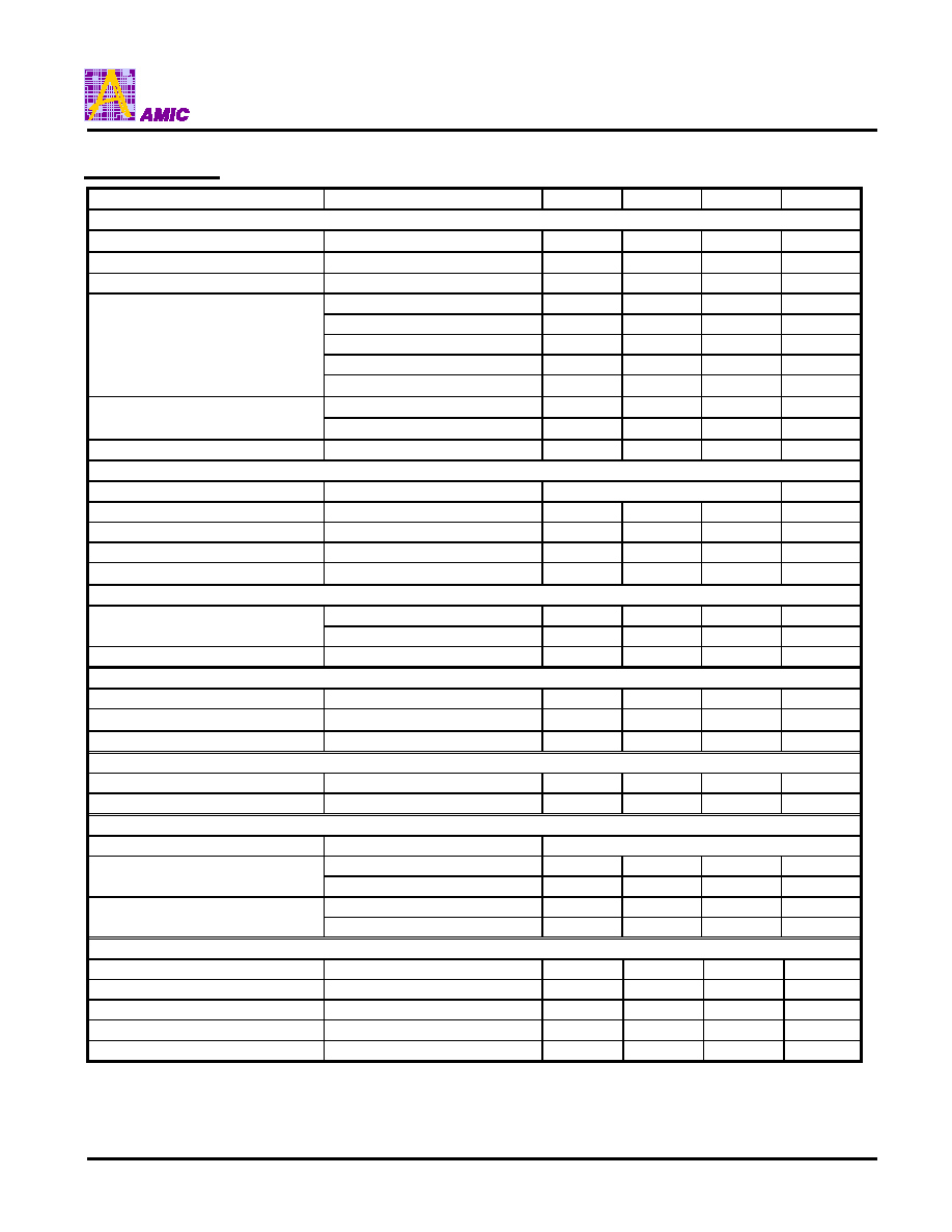
Specification
Parameter Description
Min.
Typ.
Max.
Unit
General
Storage Temperature
-20 70
�
C
Operating Temperature
0 50
�
C
Supply Voltage
2.2
2.5
5
V
Active (RX Mode)
30
mA
Active (TX Mode @high power)
17
mA
Active (TX Mode @low power)
14
mA
Stand By Mode
1.5
mA
Current Consumption
Transceiver Circuit
Sleep Mode
5
�
A
Active @VIN = 3.3V
150
�
A
Current Consumption
Embedded Regulator
Stand By
5
�
A
Phase Locked Loop
Reference Frequency
4,6,8,10,12,14,16 MHz
X'TAL Settling Time
@12MHz, cap. Load = 20pF
5
ms
Operation Frequency
2416~2478
MHz
Number of Channels
@ 2MHz spacing
32
PLL Settling Time
@Loop bandwidth = 100KHz
150
�
s
RF Front End (TX mode)
High
Power
-6
dBm
TX Power
Low Power
-16
dBm
RF Output Impedance
@2.45GHz
50
Ohm
RF Front End (RX mode)
RF Input Impedance
@2.45GHz
50
Ohm
Sensitivity
@BER
=
0.001
-80 dBm
Cascaded IIP3 TBM
-30
dBm
IF Section
Intermediate Frequency
10.7
MHz
RSSI Range
@RF input
-90
-50
dBm
Modulation / Demodulation
Scheme FSK
@ Crystal modulation
64
Kbps
Data rate
@ VCO modulation
100
Kbps
@ Crystal modulation
50 KHz
Frequency Deviation
@ VCO modulation
150 KHz
Regulator
Supply voltage
5
V
Output voltage
2.5
V
Drop out voltage
0.2
V
Load current
50
mA
Battery-Low indicator reference
1.2
V
Table 1.

A7101
PRELIMINARY (March 2004, Version 0.4)
4
AMIC Technology, Corp.
RF - Baseband Interface
Pin Number
Pin Name
Description
Note
23 VIN
Supply
voltage.
GND
Ground.
Please see Pin Descriptions
section for detail.
7
TXDATAIN
Transmitter data input.
2 RXDATA
Receiver
data
output.
17
SPI_DATA
Data for SPI interface.
18
SPI_CLOCK
Clock for SPI interface.
19
SPI_LATCH
Latch for SPI interface.
20
MODSEL0
Chip operation mode selection (LSB).
Option.
24
MODSEL1
Chip operation mode selection (MSB).
Option.
25
LD
PLL locked detect Indicator output.
Option.
22
EN_REG
Voltage regulator enable pin.
Option.
13 LVOUT
Battery-low
indicator output.
Option.
37
MUTE
Receiver mute control output pin.
Option.
47
EN_AFC
AFC circuit control pin.
Option.
Table 2.