 | ÐлекÑÑоннÑй компоненÑ: A7301 | СкаÑаÑÑ:  PDF PDF  ZIP ZIP |
þÿ

A7301
Preliminary
2.4GHz FSK Transmitter
PRELIMINARY (October, 2003, Version 0.6)
AMIC Technology, Corp.
Document Title
2.4GHz FSK Transmitter
Revision History
Rev. No.
History
Issue Date
Remark
0.0
Initial issue
January 3, 2002
Preliminary
0.1
Error correction:
February 4, 2002
Change part number from A73P24P01 to A73P024P01
0.2
Modify AC Characteristic, PIN description and SPI interface
July 30, 2002
0.3
Update Fig-3, 4, 7and 8. Table-3 and pin description.
August 2, 2002
0.4
Modify frequency deviation, data rate, output power, low voltage
October 16, 2002
indicator SPI interface, and pin description.
0.5
Modify X'TAL Settling Time, Tx output power (Low power)
June 9, 2003
Application Circuit, and delete X'TAL accuracy
0.6
Improve Performance
October 6, 2003
Important Notice:
AMIC reserves the right to make changes to its products or to discontinue any integrated circuit product or
service without notice. AMIC integrated circuit products are not designed, intended, authorized, or warranted to
be suitable for use in life-support applications, devices or systems or other critical applications. Use of AMIC
products in such applications is understood to be fully at the risk of the customer.
A7301
Preliminary
2.4GHz FSK Transmitter
PRELIMINARY (October, 2003, Version 0.6)
1
AMIC Technology, Corp.
Typical Applications
n
Wireless Mouse and Keyboard
n
2.4GHz ISM Band Communication System
n
Wireless toy
n
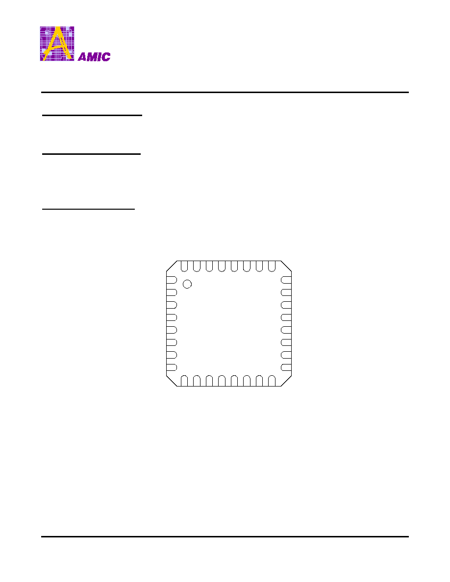
Available in 32-pin QFN package
General Description
The A7301 is a monolithic CMOS integrated circuit
intended for use as a low cost FSK transmitter in wireless
applications. The device is provided in a 32-lead plastic
QFN5X5 packaging and is designed as a complete FSK
transmitter. It is intended for wireless applications in the
2.4GHz to 2.5GHz ISM band. The chip features a fully
programmable frequency synthesizer with integrated VCO
circuitry.
Pin Configurations
1
2
3
4
5
6
7
8
9
10
11
12
13
14
15
16
24
23
22
21
20
19
18
17
32
31
30
29
28
27
26
25
NC
TXDATAIN
NC
XTAL1
XTAL2
XTALOUT
CAPSW
NC
CHPOUT
LD
MODSEL1
MODSEL0
VDD_D
VIN
REGFB
BR_VCO
BP_REG
LVOUT
LVIN
VOUT
SPI_DATA
SPI_CLOCK
SPI_LATCH
EN_REG
NC
BP_PA
VDD_A
RFOUT
BP_BUF
VDD_VCO
BP_VCO
VT
A7301
Figure 1. QFN Package Top View
A7301
PRELIMINARY (October, 2003, Version 0.6)
2
AMIC Technology, Corp.
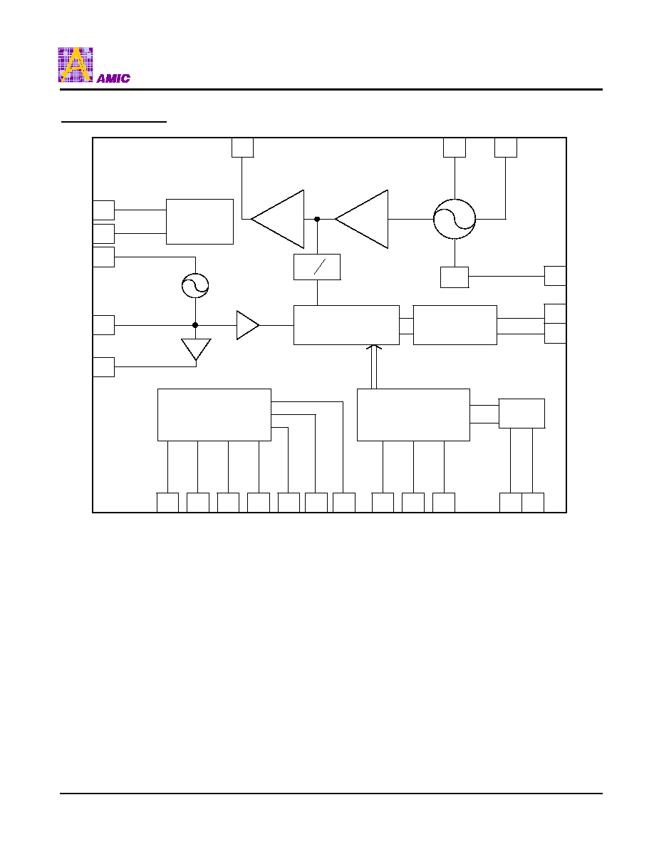
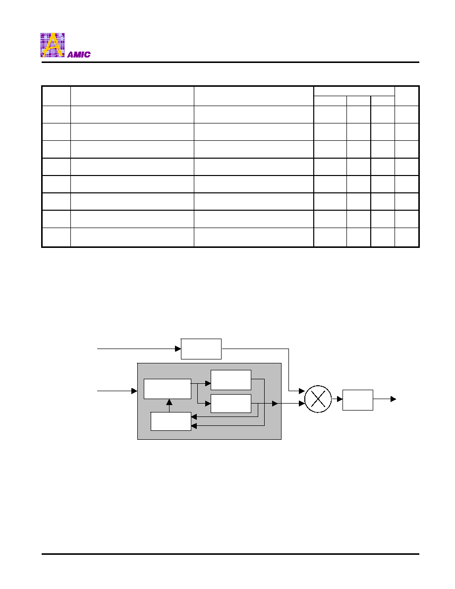
Block Diagram
SPI_CLOCK
TXDATAIN
CAPSW
MODSEL0
LD
MODSEL1
CHPOUT
BR_VCO
VT
BP_VCO
RFOUT
SPI_LATCH
SPI_DATA
XTAL1
XTAL2
XTALOUT
BP_REG
LVOUT
LVIN
VOUT
EN_REG
REGFB
VIN
VCO
OSC
29
26
25
24
23
22
21
20
15
14
13
18
17
16
12
11
10
9
SPI
Phase Detector
Charge Pump
Bias
Counter
33
32
÷
Buffer
6
5
4
7
2
PA
FSK
Modulation
Circuit
Voltage Regulator &
Low voltage detector
Mode
Selection
Figure 2. System Block Diagram
A7301
PRELIMINARY (October, 2003, Version 0.6)
3
AMIC Technology, Corp.
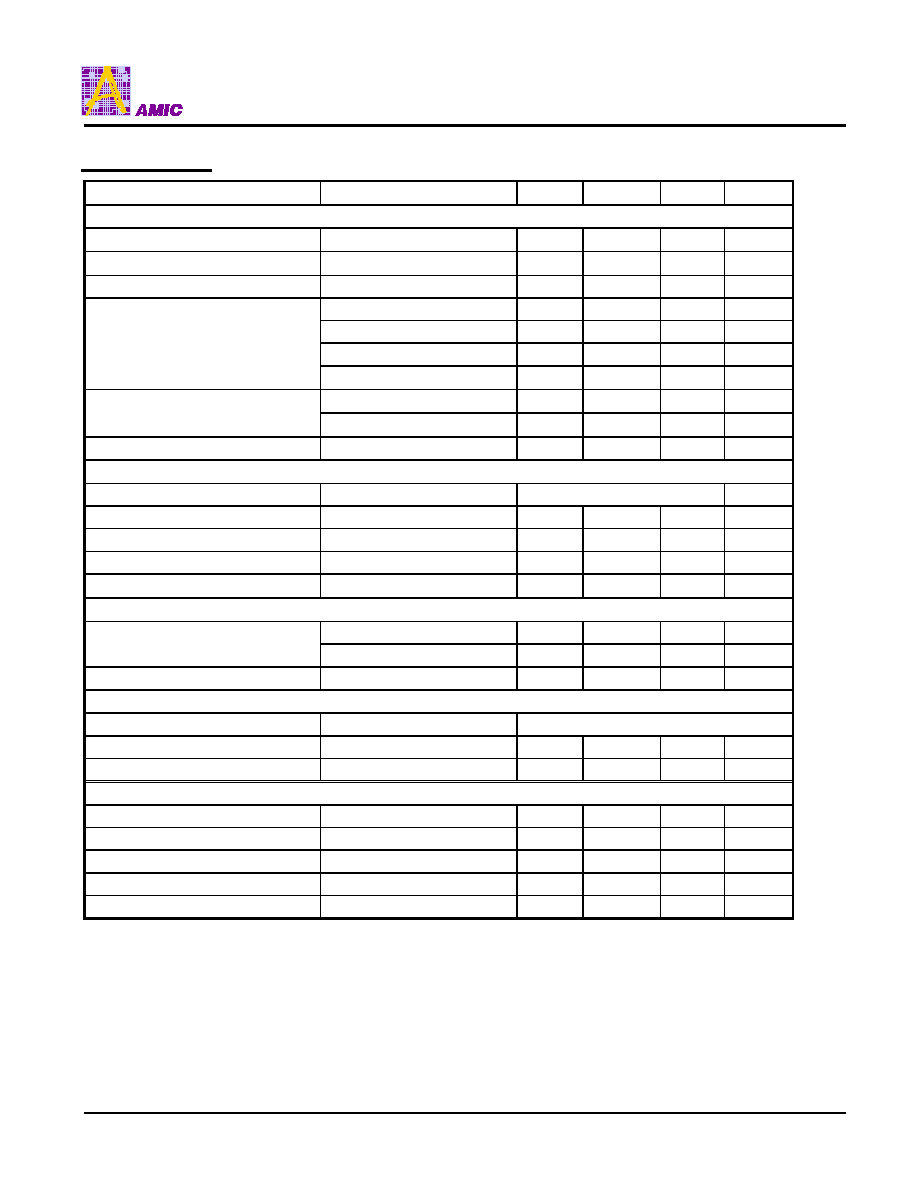
Specification
Parameter
Description
Min.
Typ.
Max.
Unit
General
Storage Temperature
-20
70
°
C
Operation Temperature
0
50
°
C
Supply Voltage
2.2
2.5
5
V
Active (@High Power)
17
mA
Active (@Low Power)
14
mA
Stand By
1.5
mA
Current Consumption
Transmitter Circuit
Sleep
5
µ
A
Active @ Vin = 3.3V
150
µ
A
Current Consumption
Embedded Regulator
Stand By
5
µ
A
Average Current Consumption
@25% Duty, Low Power
5
mA
Phase Locked Loop
Reference Frequency
4,6,8,10,12,14,16
MHz
X'TAL Settling Time
@12MHz, cap. Load = 20pF
5
ms
Operation Frequency
2416~2478
MHz
Number of Channel
@2MHz spacing
32
PLL Settling Time
@Loop bandwidth = 100KHz
150
µ
s
RF Front End
High Power
-2
dBm
TX Power
Low Power
-10
dBm
RF Output Impedance
@2.45GHz
50
Ohm
Modulation
Scheme
FSK
Frequency Deviation
+/-
50
KHz
Data Rate
4.8
64
Kbps
Regulator
Supply voltage
5
V
Output voltage
2.5
V
Drop out voltage
0.2
V
Load current
50
mA
Battery-Low indicator reference
1.2
V
Table 1.

A7301
PRELIMINARY (October, 2003, Version 0.6)
4
AMIC Technology, Corp.
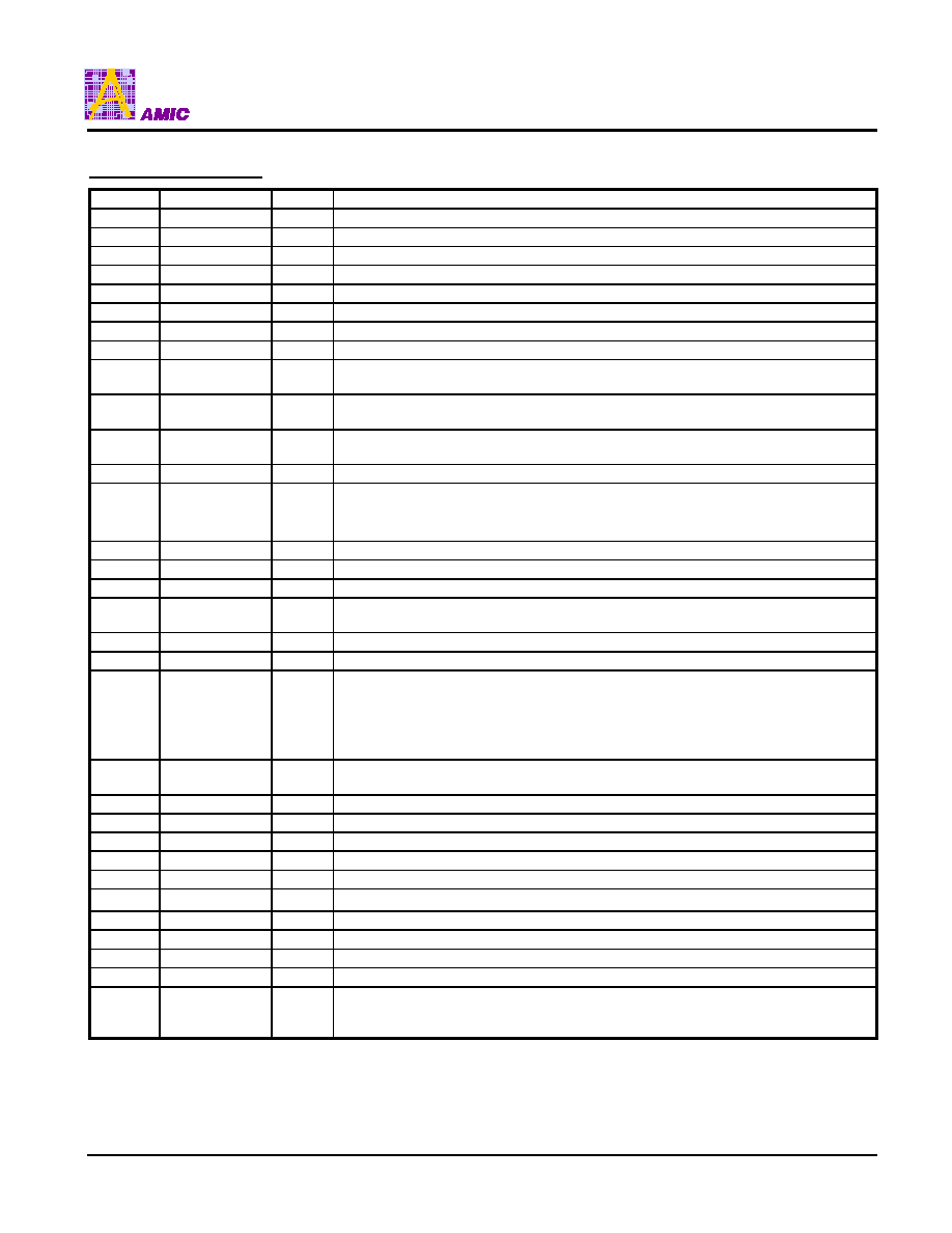
RF - Baseband Interface
Pin Number
Pin Name
Description
Note
18
VIN
Supply voltage.
GND
Ground.
Please see Pin Descriptions
section for detail.
2
TXDATAIN
Transmitter data input.
13
SPI_DATA
Data for SPI interface.
14
SPI_CLOCK
Clock for SPI interface.
15
SPI_LATCH
Latch for SPI interface.
20
MODSEL0
Chip operating mode selection (LSB).
Option.
21
MODESEL1
Chip operating mode selection (MSB).
Option.
22
LD
PLL locked detect indicator output.
Option.
16
EN_REG
Voltage regulator enable pin.
Option.
10
LVOUT
Battery-low indicator output.
Option.
Table 2.
A7301
PRELIMINARY (October, 2003, Version 0.6)
5
AMIC Technology, Corp.
Pin Descriptions
(I: input; O: output; OD: open drain output)
Pin No.
Symbol
I/O
Function Description
1
NC
This pin must be open.
2
TXDATAIN
I
Transmitter data input.
3
NC
This pin must be open.
4
XTAL1
I
Colpitts crystal oscillator node 1. Connect to external feedback capacitor.
5
XTAL2
I
Colpitts crystal oscillator node 2. Connect to external feedback capacitor.
6
XTALOUT
O
Inverted output from crystal oscillator.
7
CAPSW
I
Modulation switch input.
8
NC
This pin must be open.
9
BP_REG
O
Regulator band gap bypass output. Connect to external noise rejection capacitor.
Typical output voltage is 1.2V.
10
LVOUT
O
Battery-Low voltage indicator output. This pin is active low when LVIN is below
BP_REG voltage level.
11
LVIN
I
Input for battery-low voltage indicator. The indicator compares LVIN with the threshold
voltage, BP_REG.
12
VOUT
O
Regulator output voltage. Nominal voltage output is 2.5V.
13
SPI_DATA
I/OD
Data for SPI interface.
This pin operates as an Input pin when SPI is in Write mode. This pin operates as an
open drain output when SPI is in Read mode.
14
SPI_CLOCK
I
Clock input for SPI interface.
15
SPI_LATCH
I
Latch input for SPI interface.
16
EN_REG
I
Voltage regulator enable pin. Signal is active high.
17
REGFB
O
Output from regulator feedback network. VOUT is set to nominal voltage when this pin
is opened. If other voltage is required, connect it to external resistor to adjust VOUT.
18
VIN
I
Supply voltage for the internal voltage regulator.
19
VDD_D
I
Digital supply voltage input.
20
21
MODSEL0
MODSEL1
I
Transmitter (embedded regulator not included) operation mode selection inputs.
MODSEL[1:0] = 00: Sleep mode. Transmitter circuit is turned off.
MODSEL[1:0] = 01: Stand-by mode. X'TAL oscillator is turned on.
MODSEL[1:0] = 10: Transmit mode.
MODSEL[1:0] = 11: Reserved.
22
LD
OD
Output from PLL lock detector. This pin is active high (Open drain) when PLL is
locked.
23
CHPOUT
O
Charge-pump output. This pin charges external capacitor to adjust VCO frequency.
24
BR_VCO
O
VCO band gap bias output. Connect to external resistor to set bias current.
25
VT
I
VCO tuning voltage input. The VCO frequency increases as VT increases.
26
BP_VCO
O
Noise bypass. Connect to external noise rejection capacitor.
27
VDD_VCO
I
VCO supply voltage input.
28
BP_BUF
O
Noise bypass. Connect to external noise rejection capacitor.
29
RFOUT
O
RF output with internal 4Kohm pull down resistor.
30
VDD_A
I
Analog supply voltage input.
31
BP_PA
O
Noise bypass.
32
NC
This pin must leave open.
GND
All internal groundings are connected through the paddle on the back-side of the IC.
It is important to make sure proper ground soldering during SMT process to ensure
solid grounding path to the target PCB.
Table 3.

A7301
PRELIMINARY (October, 2003, Version 0.6)
6
AMIC Technology, Corp.
Absolute Maximum Ratings
Parameter
With respect to
Rating
Unit
Supply voltage range (VDD)
GND
-0.3 to 5.5
Vdc
Other I/O pins range
GND
-0.3 to VDD+0.3
Vdc
Storage temperature range
-20 ~ +70
°
C
Table 4.
*Stresses above those listed under "Absolute Maximum Rating" may cause permanent damage to the device. These are stress
ratings only; functional operation of the device at these or any other conditions above those indicated in the operational
sections of this specification is not implied. Exposure to absolute-maximum-rated conditions for extended periods may affect
device reliability.
A7301
PRELIMINARY (October, 2003, Version 0.6)
7
AMIC Technology, Corp.
Circuit Description
1. Reset
When SPI_CLOCK and SPI _LATCH are both held high simultaneously, bit 4 through bit 9 of the Mode Select Register will be
reset to "Low" state.
2. Serial to Parallel Interface (SPI)
A7301's SPI bus consists of three signals: SPI_DATA, SPI_CLOCK, and SPI_LATCH. This interface is used for external
base-band controller to communicate with transmitter's internal data and control registers. The contents of the registers are
shown in the following register description sections.
After setting SPI_LATCH signal to "Low" state, data on SPI_DATA is shifted into the internal shift register on the rising edge of
SPI_CLOCK with MSB going in first. SPI_LATCH should be asserted at the end to latch the data packet into the register
according to the address bits, bit 0 through bit 3, for each of the registers. All registers can only be written into except the
Status Register that can only be read.
When the content of the Status Register need to be fetched by external controller, external baseband controller need to make
sure that the address bits are pointing to address location 0x0 for proper read operation. After the address bits are shifted into
the SPI interface and latched by asserting SPI_LATCH, the SPI interface will be in Read Mode and the content of the Status
Register will be shifted out on SPI_DATA pin. When all 12-status bits have been shifted out, SPI bus will be put back to Write
Mode automatically.
A.
Register Description
Note: Convention used:
1: Logic level "ONE".
0: Logic level "ZERO".
X: Don't care.
Synthesizer Configuration Register I (Write only / Address 0xf)
Bit 15 Bit 14 Bit 13 Bit12 Bit11 Bit10
Bit9
Bit8
Bit7
Bit6
Bit5
Bit4
Bit3
Bit2
Bit 1
Bit 0
MB6
MB5
MB4
MB3
MB2
MB1
MB0
MA4
MA3
MA2
MA1
MA0
1
1
1
1
Synthesizer Configuration Register II (Write only / Address 0x7)
Bit 15 Bit 14 Bit 13 Bit12 Bit11 Bit10
Bit9
Bit8
Bit7
Bit6
Bit5
Bit4
Bit3
Bit2
Bit 1
Bit 0
X
MB9
MB8
MB7
R7
R6
R5
R4
R3
R2
R1
R0
0
1
1
1
Synthesizer Configuration Register I and Synthesizer Configuration Register II control synthesizer frequency settings where
MA[4:0]: A counter[4:0],
MB[9:0]: B counter[9:0],
R[7:0]: R counter[7:0]. Valid range is from 2 to 255.
The content of A, B and R registers are in unsigned binary format (i.e., 11111
2
= 31
10
)
The equation for setting the synthesizer frequency is:
f
vco
= f
crystal
X (32 X B + A) / R (B must be greater than A).
A7301
PRELIMINARY (October, 2003, Version 0.6)
8
AMIC Technology, Corp.
Crystal Control Register (Write only / Address 0xb)
Bit 15 Bit 14 Bit 13 Bit12 Bit11 Bit10
Bit9
Bit8
Bit7
Bit6
Bit5
Bit4
Bit3
Bit2
Bit 1
Bit 0
0
DP
TXH2 TXH1 TXH0 TXL2 TXL1 TXL0 FX3
FX2
FX1
FX0
1
0
1
1
DP: Data Polarity. This control bit sets data output polarity.
0: Inverted.
1: Normal.
TXH[2:0]: Reserved. Must be set to 0x0 for proper operation.
TXL[2:0]: Reserved. Must be set to 0x0 for proper operation.
FX[3:0]: Reserved. Must be set to 0x0 for proper operation.
VCO Control Register (Write only / Address 0x3)
Bit 15 Bit 14 Bit 13 Bit12 Bit11 Bit10
Bit9
Bit8
Bit7
Bit6
Bit5
Bit4
Bit3
Bit2
Bit 1
Bit 0
VTH2 VTH1 VTH0
T1
T0
HP0
CP2
CP1
CP0
VC2
VC1
VC0
0
0
1
1
VTH[2:0]: Set VCO tuning voltage range. Valid range is from 0x7 to 0x0. The setting of VTH varies inversely with the tuning
voltage range such that when VTH = 0x0 tuning voltage range is from 0.3V to VDD-0.3V and when VTH = 0x7 tuning voltage
range is from 1V to VDD-1V.
T[1:0]: Reserved. Must be set to 0x0 for proper operation.
HP0: RF output power level control.
0: Low power output.
1: High power output.
CP[2]: Reserved. Must be set to 0x0 for proper operation.
CP[1:0]: Charge pump output current control. Valid range is from 0x3 to 0x0. The setting of CP varies linearly with the output
current level such that when CP = 0x0 output current = 100uA and when CP = 0x3 output current = 700uA.
VC[2:0]: Reserved. Must be set to 0x4 for proper operation.
Test Control Register (Write only / Address 0xd)
Bit 15 Bit 14 Bit 13 Bit12 Bit11 Bit10
Bit9
Bit8
Bit7
Bit6
Bit5
Bit4
Bit3
Bit2
Bit 1
Bit 0
T2
T1
T0
X
X
X
X
X
X
X
X
X
1
1
0
1
T[2:0]: Reserved. Must be set to 0x1 for proper operation.
A7301
PRELIMINARY (October, 2003, Version 0.6)
9
AMIC Technology, Corp.
Mode Select Register (Write only / Address 0x5)
Bit 15 Bit 14 Bit 13 Bit12 Bit11 Bit10
Bit9
Bit8
Bit7
Bit6
Bit5
Bit4
Bit3
Bit2
Bit 1
Bit 0
X
X
X
X
X
SC1
SC0
X
CM
EXTB MD1 MD0
0
1
0
1
SC[1:0]: Status Register bit 6 control. Depends on the setting of SC[1:0], bit 6 of the Status Register can represent either
system error flag, Battery-low detect or PLL lock detect.
[1:0] = 10: System Error.
[1:0] = 11: Battery-low detect.
[1:0] = 0X: PLL lock detect.
CM: Reserved. Must be set to 1 for proper operation.
EXTB: Operating mode selection.
0: external mode. Mode of operation is determined by external pin MODSEL0 and MODSEL1.
1: internal mode. Mode of operation is determined by MD[1:0].
MD[1:0]: Internal mode selection.
[1:0] = 00: Sleep mode. Transmitter circuit is turned off.
[1:0] = 01: Stand-by mode. X'TAL oscillator is turned on.
[1:0] = 10: Transmit mode.
[1:0] = 11: Reserved.
Status Register (Read only / Address 0x0)
SR15 SR14 SR13 SR12 SR11 SR10 SR9
SR8
SR7
SR6
SR5
SR4
SR3
SR2
SR1
SR0
X
X
X
X
X
X
X
X
X
S/B/P
X
X
0
0
0
0
S/B/P: Depends on the setting of SC[1:0] in Mode Select Register, this bit can be used to reflect the status of System Error,
Battery-low detect or PLL lock detect.
System Error: 0: Normal; 1: Error.
Battery-low detect: 0: Battery supply voltage below threshold; 1: Normal.
PLL lock detect: 0: Unlock; 1: Lock.
SR[3:0] address bits.
A7301
PRELIMINARY (October, 2003, Version 0.6)
10
AMIC Technology, Corp.
B.
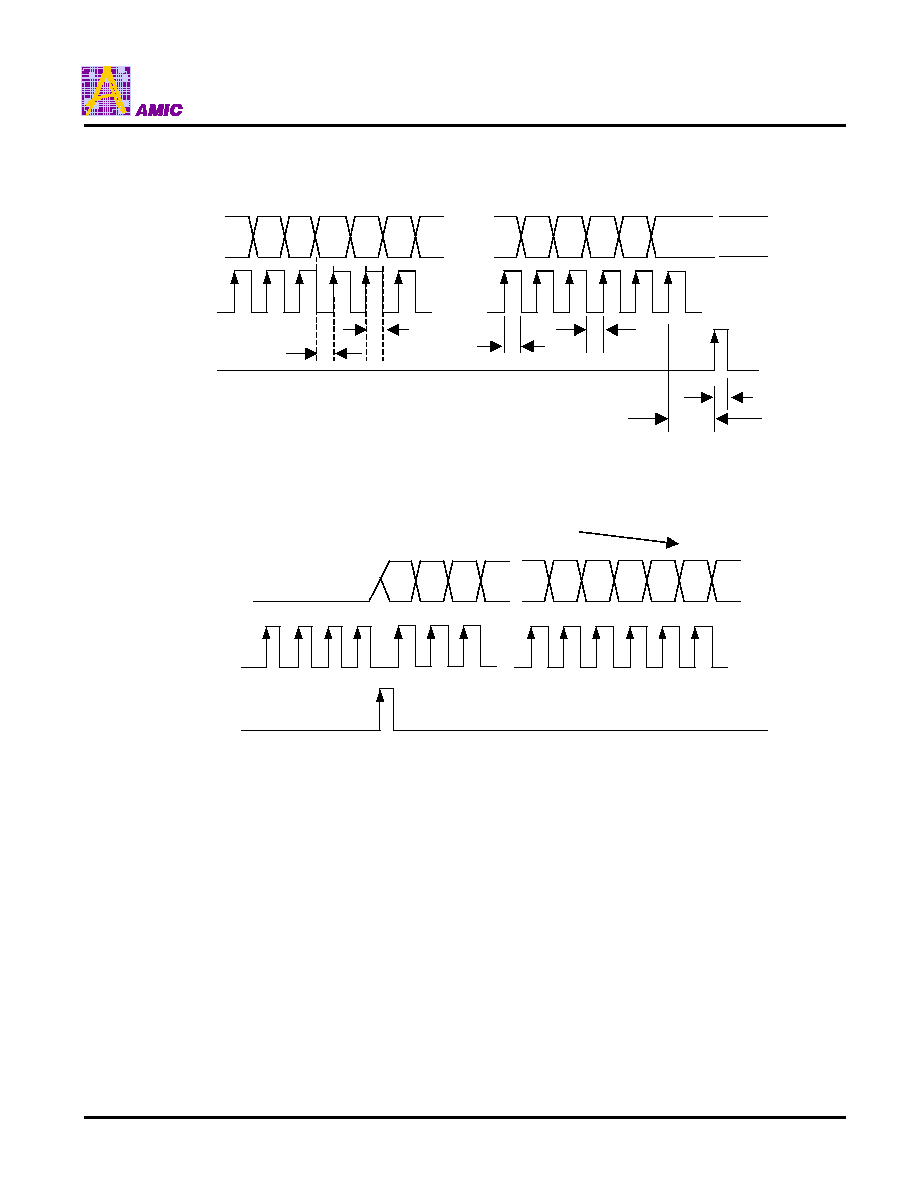
SPI Timing Diagram
Figure 3. SPI WRITE mode timing diagram
Figure 4. SPI READ mode timing diagram
t
CWL
t
CWH
t
CS
t
CH
t
ES
t
EW
SPI_DATA
SPI_CLOCK
SPI_LATCH
V
H
V
l
Bit15 Bit14 Bit13 Bit12 Bit11 Bit10 Bit9 Bit5 Bit4 Bit3 Bit2 Bit1 Bit0
SPI_DATA
SPI_CLOCK
SPI_LATCH
SR0 SR1 SR2 SR3 SR4 SR5 SR6 SR7 SR11 SR12 SR13 SR14 SR15 Bit15 Bit14
After reading 12 bits, SPI set to write mode
A7301
PRELIMINARY (October, 2003, Version 0.6)
11
AMIC Technology, Corp.
C.
SPI Timing Specification
Value
Symbol
Parameter
Conditions
Min
Typ
Max
Units
V
H
The High level of voltage
Three wire SPI_CLOCK, SPI_DATA,
SPI_LATCH timing diagram
VCC-0.4
V
V
l
The low level of voltage
Three wire SPI_CLOCK, SPI_DATA,
SPI_LATCH timing diagram
0.4
V
t
CS
SPI_DATA to SPI_CLOCK setup time
Three wire SPI_CLOCK, SPI_DATA,
SPI_LATCH timing diagram
50
ns
t
CH
SPI_CLOCK to SPI_DATA hold time
Three wire SPI_CLOCK, SPI_DATA,
SPI_LATCH timing diagram
10
ns
t
CWH
SPI_CLOCK pulse width high
Three wire SPI_CLOCK, SPI_DATA,
SPI_LATCH timing diagram
50
ns
t
CWL
SPI_CLOCK pulse width low
Three wire SPI_CLOCK, SPI_DATA,
SPI_LATCH timing diagram
50
ns
t
ES
SPI_CLOCK to SPI_LATCH setup time
Three wire SPI_CLOCK, SPI_DATA,
SPI_LATCH timing diagram
50
ns
t
EW
SPI_LATCH pulse width
Three wire SPI_CLOCK, SPI_DATA,
SPI_LATCH timing diagram
50
ns
Table 5.
3. PLL Section
The Phase Lock Loop block is shown as follows:
Figure 5. Phase Lock Loop Block Diagram
Phase Detector
Charge
Pump
B Counter
10 bit
PRESCALER
32/33
A Counter
5 bit
Control Logic
R Counter
8 bit
VCO input
CHPOUT
Input from reference
crystal OSC.
M Counter
A7301
PRELIMINARY (October, 2003, Version 0.6)
12
AMIC Technology, Corp.
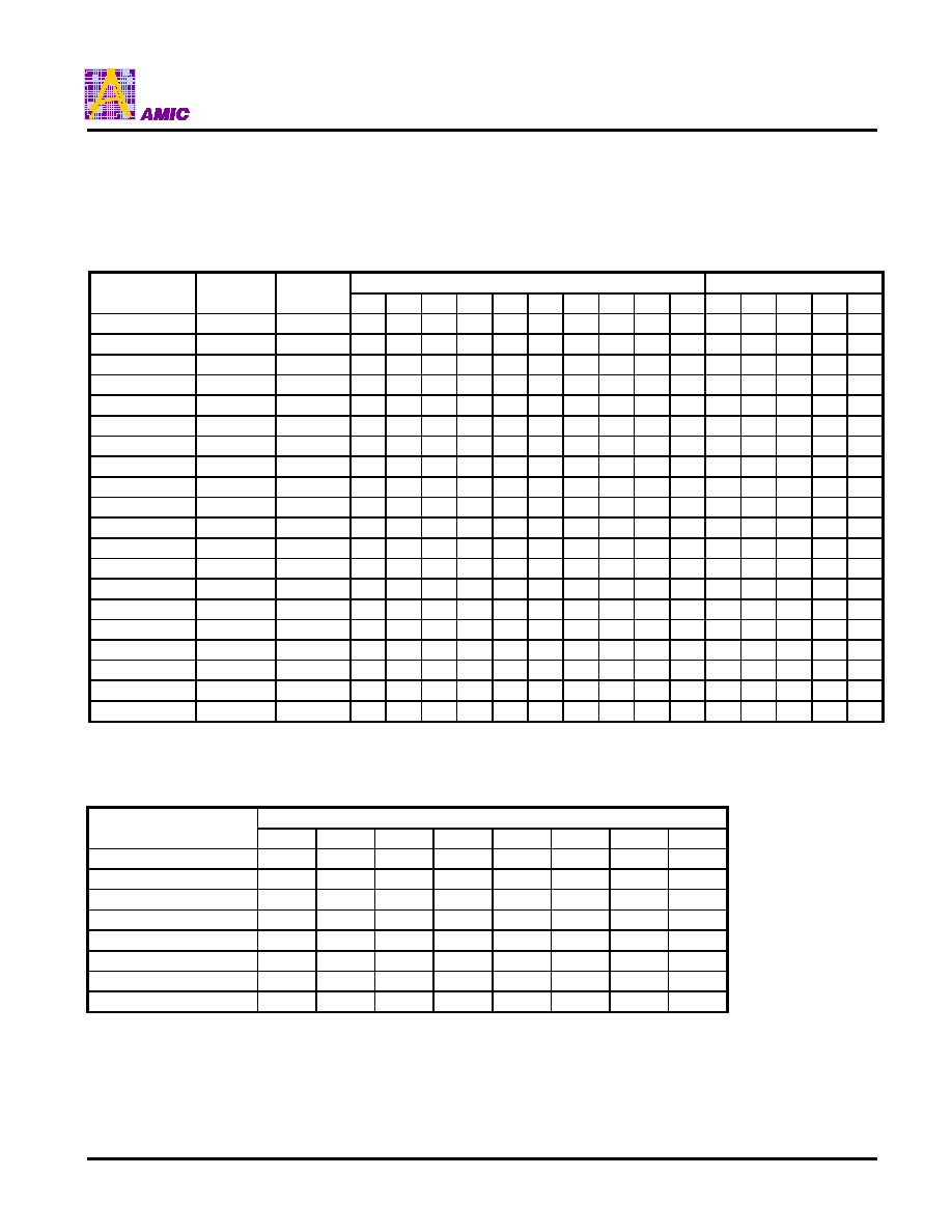
A. M Counter
The M counter consists of a 32/33 pre-scalar, a 5-bit A counter and a 10-bit B counter (where M = B*32+A).
B. A and B Counters
The A and B counters can be programmed through the
Synthesizer Configuration Register I and II. The corresponding
relations between the division ratio counters and Synthesizer Configuration Register are shown in the following table:
M counter
B counter A counter
B counter (binary)
A counter (binary)
(DEC)
(DEC)
(DEC)
MB9 MB8 MB7 MB6 MB5 MB4 MB3 MB2 MB1 MB0 MA4 MA3 MA2 MA1 MA0
2400
75
0
0
0
0
1
0
0
1
0
1
1
0
0
0
0
0
2401
75
1
0
0
0
1
0
0
1
0
1
1
0
0
0
0
1
.
.
.
0
0
0
1
.
.
.
.
.
.
.
.
.
.
.
2431
75
31
0
0
0
1
0
0
1
0
1
1
1
1
1
1
1
2432
76
0
0
0
0
1
0
0
1
1
0
0
0
0
0
0
0
2433
76
1
0
0
0
1
0
0
1
1
0
0
0
0
0
0
1
.
.
.
0
0
0
1
.
.
.
.
.
.
.
.
.
.
.
2463
76
31
0
0
0
1
0
0
1
1
0
0
1
1
1
1
1
2464
77
0
0
0
0
1
0
0
1
1
0
1
0
0
0
0
0
.
.
.
.
.
.
.
.
.
.
.
.
.
.
.
.
.
.
.
.
.
.
.
.
.
.
.
.
2492
77
28
0
0
0
1
0
0
1
1
0
1
1
1
1
0
0
2493
77
29
0
0
0
1
0
0
1
1
0
1
1
1
1
0
1
2494
77
30
0
0
0
1
0
0
1
1
0
1
1
1
1
1
0
2495
77
31
0
0
0
1
0
0
1
1
0
1
1
1
1
1
1
2496
78
0
0
0
0
1
0
0
1
1
1
0
0
0
0
0
0
2497
78
1
0
0
0
1
0
0
1
1
1
0
0
0
0
0
1
2498
78
2
0
0
0
1
0
0
1
1
1
0
0
0
0
1
0
2499
78
3
0
0
0
1
0
0
1
1
1
0
0
0
0
1
1
2500
78
4
0
0
0
1
0
0
1
1
1
0
0
0
1
0
0
Table 6.
C.
R Counter
R counter division R
R_PLL_R register bits
(DEC)
R7
R6
R5
R4
R3
R2
R1
R0
2
0
0
0
0
0
0
1
0
3
0
0
0
0
0
0
1
1
4.
0
0
0
0
0
1
0
0
.
.
253
1
1
1
1
1
1
0
1
254
1
1
1
1
1
1
1
0
255
1
1
1
1
1
1
1
1
Note: Valid range of R counter is from 2 to 255.
Table 7.
The equation for setting the synthesizer frequency is:
f
vco
= f
crystal
X (32 X B + A) / R (B must be greater than A).
A7301
PRELIMINARY (October, 2003, Version 0.6)
13
AMIC Technology, Corp.
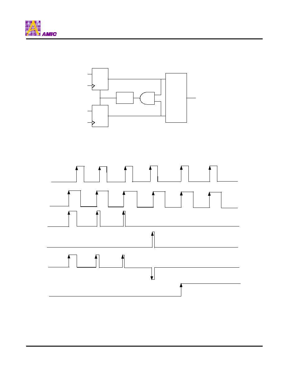
D. Phase Frequency Detector (PFD) and Charge Pump
PFD operates on outputs from the R counter and the M counter. It produces an output signal proportional to the phase and
frequency differences between R counter and M counter. The following show a simplified schematic:
Figure 6. Phase Detector Block Diagram
The PFD output waveform is shown below.
Figure 7. PFD output waveform
UP
DN
D1
Q1
CLR
D1
Q1
CLR
Charge
Pump
CHPOUT
Delay
Element
VDD
VDD
VCK
RCK
UP
DN
CHPOUT
LD
Locked
VCK
RCK
A7301
PRELIMINARY (October, 2003, Version 0.6)
14
AMIC Technology, Corp.
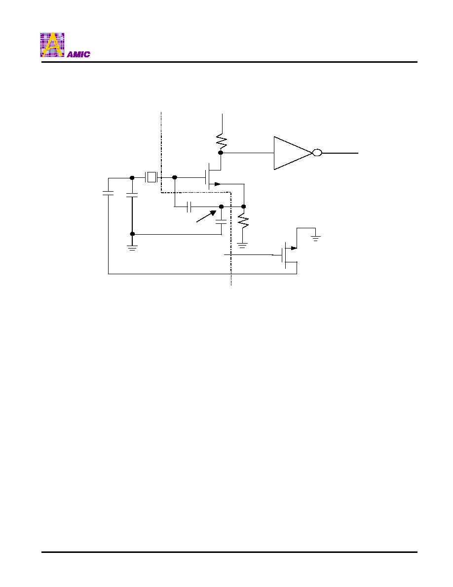
CAPSW
4. Crystal Oscillator and FSK modulation Section
As shown in the following figure, it is a Colpitts type crystal oscillator(XOSC). The FSK modulation is achieved by switching the
external capacitor C
X
in the XOSC circuit.
Figure 8. Crystal Oscillator and FSK modulation Circuit
5. Chip setup procedure:
Step 1: Supply DC voltage.
Step 2: Set Pin 20, MODSEL0 and Pin 21, MODSEL1 to logic
0 (ground) to ensure the IC is operating in external sleep
mode after reset.
Step 3: Reset IC by setting Pin 14, SPI_CLOCK and Pin 15, SPI _LATCH to logic high simultaneously for more than
1 us.
Step 4: Setup IC's internal control registers by configuring the followings: Synthesizer Configuration Register I, Synthesizer
Configuration Register II, Crystal Control Register, and Crystal Control Register. All registers should be written to in
the order specified above.
a. Synthesizer Configuration Register I and II: Set VCO center frequency.
b. Crystal Control Register: Set TXDATA polarity.
c. VCO Control Register: Set VCO tuning range and charge pump output current.
Step 5: Set IC to TX mode.
For internal mode operation, set Mode Select Register to
0x05E5.
For external mode operation, set Pin 21, MODSEL1 to "logic
1", Pin 20, MODSEL0 to "logic 0" and set Mode Select
Register to
0x05A5.
Whenever frequency is to be changed, or system error has been detected (by reading from the Status Register) the IC
must be reset by repeating step
2, 3, 4-a, and 5.
XTAL1
XTALOUT
External
Internal
XTAL2
TXDATA IN
To R counter
C
x
A7301
PRELIMINARY (October, 2003, Version 0.6)
15
AMIC Technology, Corp.
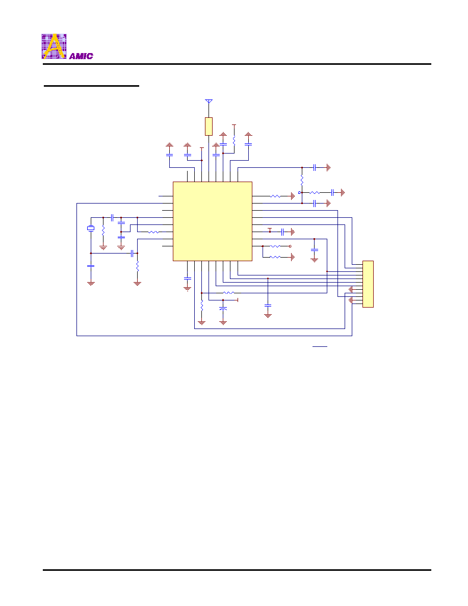
Application Circuit
NC
1
TXDATAIN
2
NC
3
XTAL1
4
XTAL2
5
XTALOUT
6
CAPSW
7
NC
8
BP_REG
9
LVOUT
10
LVIN
11
VOUT
12
SPI_DATA
13
SPI_CLOCK
14
SPI_LATCH
15
EN_REG
16
REGFB
17
VIN
18
VDD_D
19
MODSEL0
20
MODSEL1
21
LD
22
CHPOUT
23
BR_VCO
24
VT
25
BP_VCO
26
VDD_VCO
27
BP_BUF
28
RFOUT
29
VDD_A
30
BP_PA
31
NC
32
U1
A7301
R3
10K
R6 75K
R7
100K
R9
100K
R10 20K
R11
0
R12
82
C3
NC
C4 470P
C5
47P
C6
100P
C7
33P
C8
100n
C9
100n
C10
100n
C11
NC
C12
100P
C13
10P
C14
1n
C15
1u
C16
1n
C17
100n
X1
12M
C21
10u/16V
VDD
VDD
VDD
1
2
3
4
5
6
7
8
9
10
11
12
J1
CON12
VIN
GND
EN_REG
SPI_LATCH
SPI_CLOCK
SPI_DATA
MODSEL0
MODSEL1
LVOUT
TXDATAIN
VDD
IN
1
OUT
2
U2 LPF
LD
GND
C1
100p
R15
NC
R16
NC
VDD
R17
470k
C19
22P
TP
R8
3.9K
Figure 10. Application Circuit for Transmitter

A7301
PRELIMINARY (October, 2003, Version 0.6)
16
AMIC Technology, Corp.
Ordering Information
Part No.
Package
A73P024P01Q
QFN 32L
A7301
PRELIMINARY (October, 2003, Version 0.6)
17
AMIC Technology, Corp.
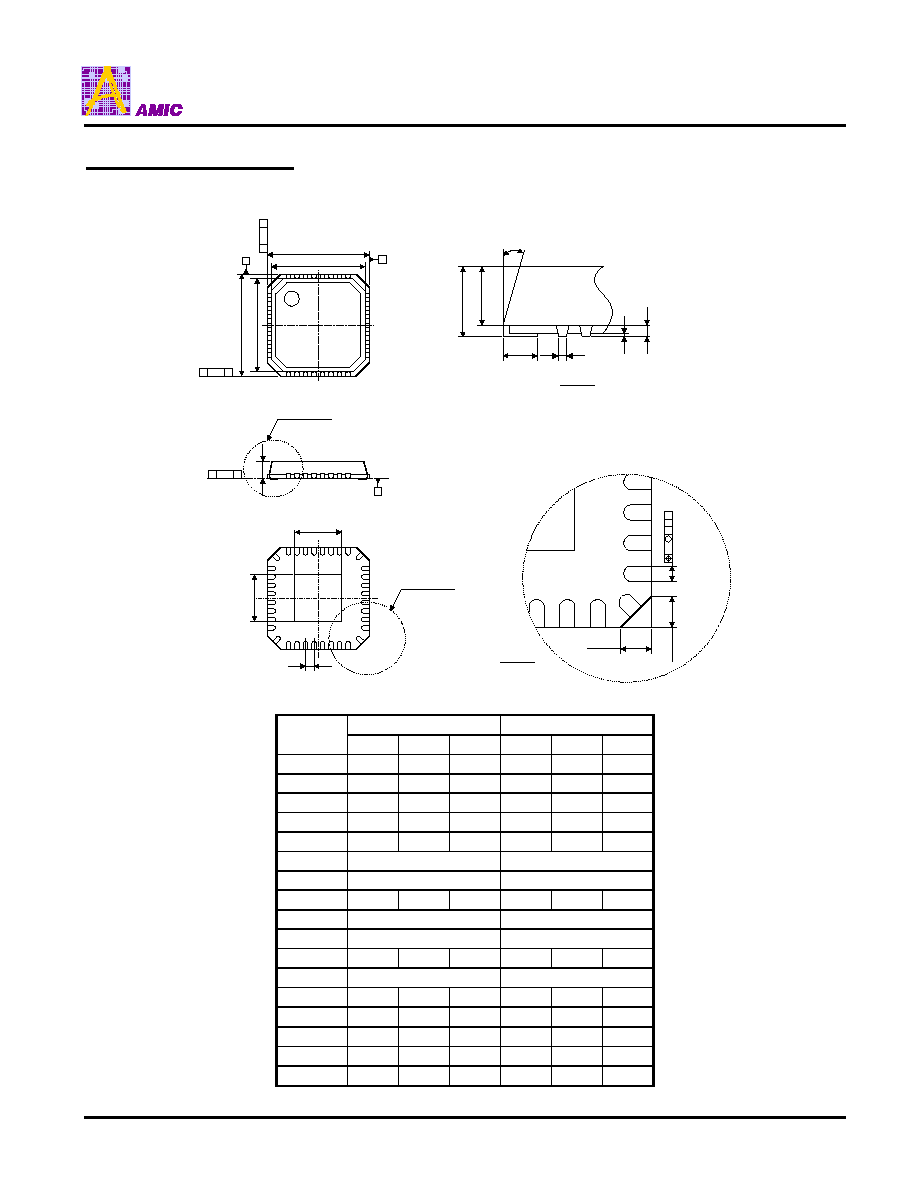
Package Information
QFN 32L Outline Dimensions
unit: inches/mm
E
E
1
D
D
1
Seating Plane
D
aaa
C
D
aaa C
B
A
D
0.08 C
A
See Detail B
A
2
A
L
b
A
1
A
3
Detail B
C
D
2
E
2
e
See Detail A
Detail A
0.6max
0.6max
b
bbb
C
M
A
B
Dimensions in inches
Dimensions in mm
Symbol
Min
Nom
Max
Min
Nom
Max
A
0.031
0.033
0.039
0.80
0.85
1.00
A
1
0.000
0.001
0.002
0.00
0.02
0.05
A
2
-
0.026
0.039
-
0.65
1.00
A
3
-
0.008
-
-
0.20
-
b
0.007
0.009
0.012
0.18
0.23
0.30
D
0.197 BSC
5.00 BSC
D
1
0.187 BSC
4.75 BSC
D
2
0.049
0.106
0.128
1.25
2.70
3.25
E
0.197 BSC
5.00 BSC
E
1
0.187 BSC
4.75 BSC
E
2
0.049
0.106
0.128
1.25
2.70
3.25
e
0.020 BSC
0.5 BSC
L
0.012
0.016
0.020
0.30
0.40
0.50
0°
-
12°
0°
-
12°
aaa
-
-
0.010
-
-
0.25
bbb
-
-
0.004
-
-
0.10
chamfer
-
-
0.024
-
-
0.60