A81L801
Stacked Multi-chip Package (MCP) 1 M X 8 Bit / 512K X 16 Bit
Boot Sector Flash Memory and 128K x 8 Bit Low Voltage CMOS SRAM
Preliminary
PRELIMINARY (March, 2005, Version 0.0)
1
AMIC Technology, Corp.
MCP Features
Single power supply operation 2.7 to 3.6 volt
High Performance
- Access time as fast as 70ns
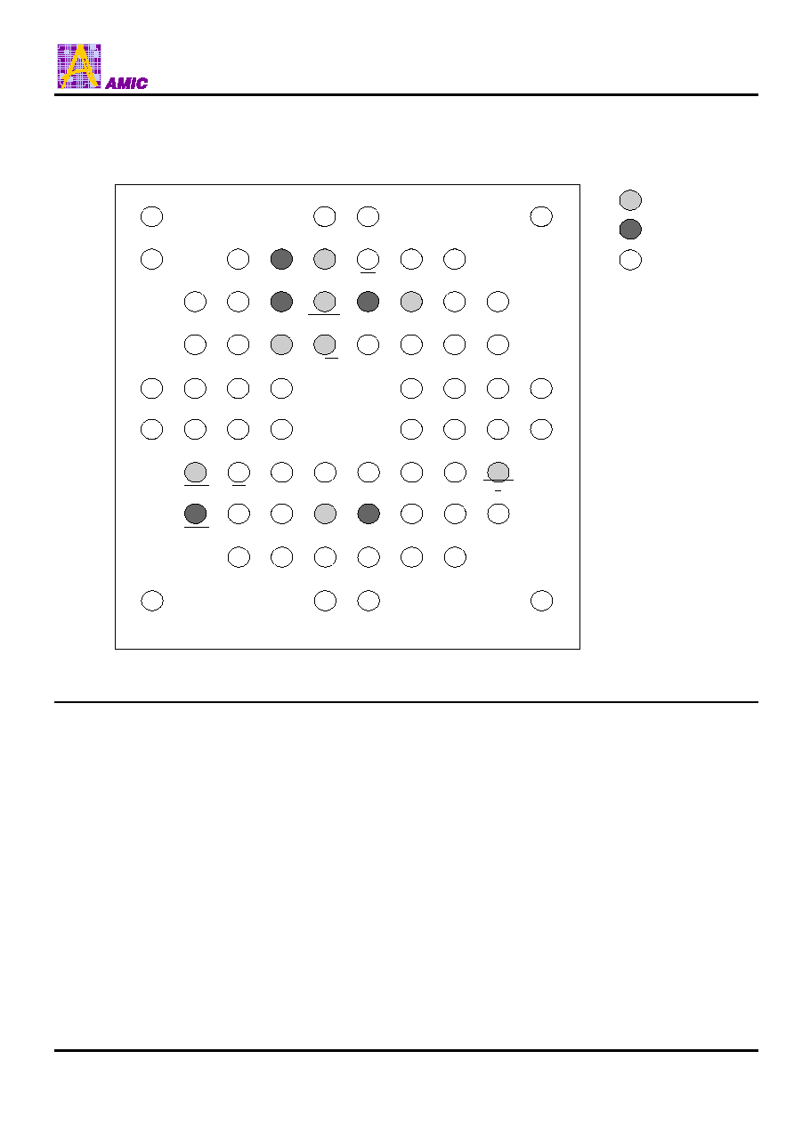
Package
-
69-Ball FBGA (8x11x1.4 mm)
Industrial operating temperature range: -25
�
C to 85
�
C for �I
Flash Features
Single power supply operation
- Full voltage range: 2.7 to 3.6 volt read and write
operations for battery-powered applications
Access times:
-
70 (max.)
Current:
- 9 mA typical active read current
- 20 mA typical program/erase current
-
200 nA typical CMOS standby
-
200 nA Automatic Sleep Mode current
Flexible sector architecture
-
16 Kbyte/ 8 KbyteX2/ 32 Kbyte/ 64 KbyteX15 sectors
-
8 Kword/ 4 KwordX2/ 16 Kword/ 32 KwordX15 sectors
-
Any combination of sectors can be erased
-
Supports full chip erase
-
Sector protection:
A hardware method of protecting sectors to prevent any
inadvertent program or erase operations within that sector.
Temporary Sector Unprotect feature allows code changes
in previously locked sectors
Extended operating temperature range: -25
�
C ~ +85
�
C for �
I series
Unlock Bypass Program Command
- Reduces overall programming time when issuing multiple
program command sequence
Top or bottom boot block configurations available
Embedded Algorithms
- Embedded Erase algorithm will automatically erase the
entire chip or any combination of designated sectors and
verify the erased sectors
- Embedded Program algorithm automatically writes and
verifies data at specified addresses
Typical 100,000 program/erase cycles per sector
20-year data retention at 125
�
C
-
Reliable operation for the life of the system
Data
Polling and toggle bits
-
Provides a software method of detecting completion of
program or erase operations
Ready /
BUSY
pin (RY /
BY
)
- Provides a hardware method of detecting completion of
program or erase operations
Erase Suspend/Erase Resume
-
Suspends a sector erase operation to read data from, or
program data to, a non-erasing sector, then resumes the
erase operation
Hardware reset pin (
RESET
)
-
Hardware method to reset the device to reading array data
LP SRAM Features
Power supply range: 2.7V to 3.6V
Access times: 70 ns (max.)
Current:
Very low power version: Operating: 30mA(max.)
Standby: 5uA (max.)
Full static operation, no clock or refreshing required
All inputs and outputs are directly TTL-compatible
Common I/O using three-state output
Output enable and two chips enable inputs for easy
application
Data retention voltage: 2.0V (min.)

A81L801
PRELIMINARY (March, 2005, Version 0.0)
2
AMIC Technology, Corp.
General Description
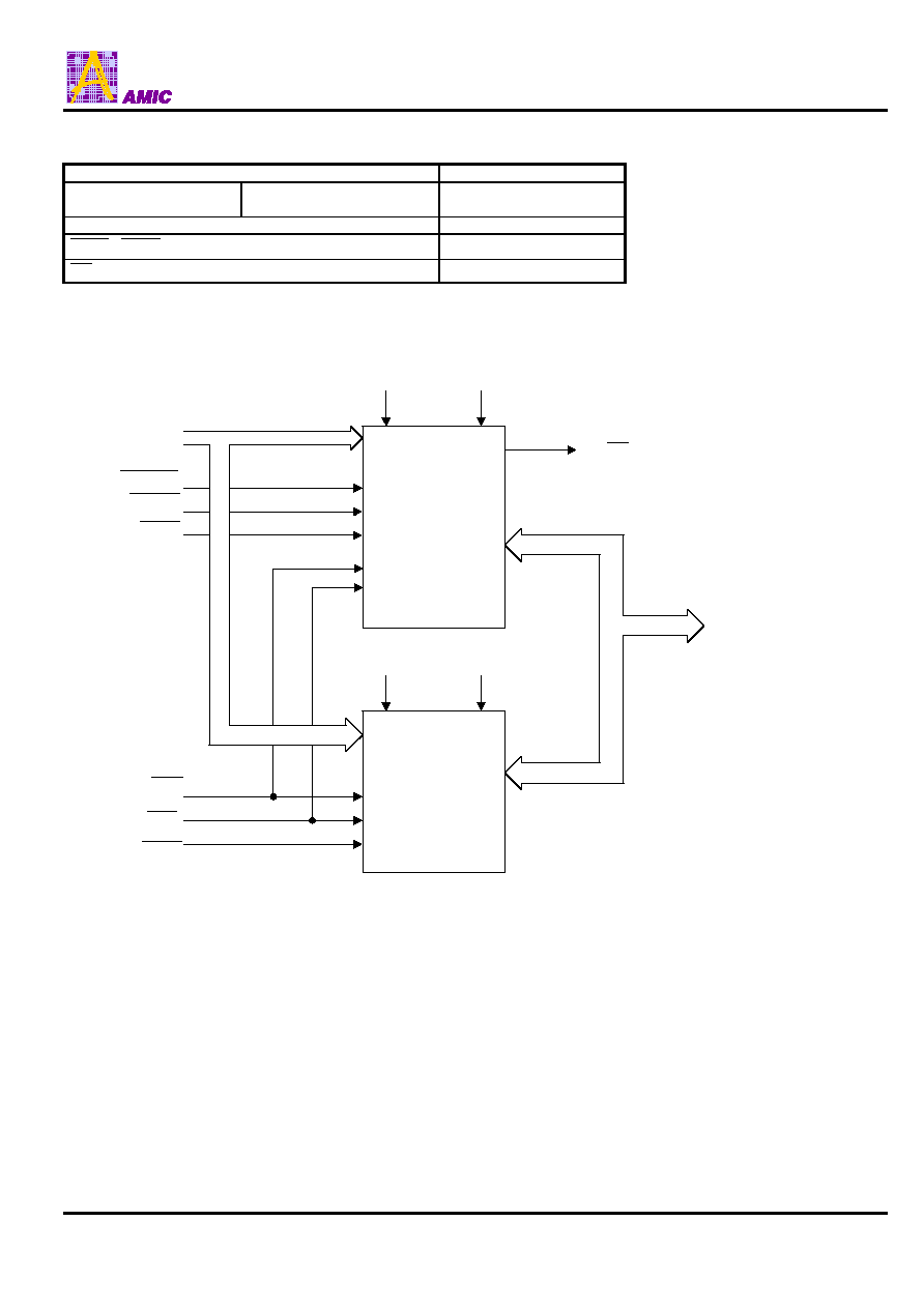
The Flash memory of A81L801 is an 8Mbit, 3.0 volt-only
memory organized as 1,048,576 bytes of 8 bits or 524,288
words of 16 bits each. The 8 bits of data appear on I/O
0
- I/O
7
;
the 16 bits of data appear on I/O
0
~I/O
15
. The A81L801 is
offered in 69-ball TFBGA package. This device is designed to
be programmed in-system with the standard system 3.0 volt
VCC supply. Additional 12.0 volt VPP is not required for in-
system write or erase operations. However, the A81L801 can
also be programmed in standard EPROM programmers.
The Flash memory of A81L801 has the first toggle bit, I/O
6
,
which indicates whether an Embedded Program or Erase is in
progress, or it is in the Erase Suspend. Besides the I/O
6
toggle
bit, the Flash memory of A81L801 also has a second toggle
bit, I/O
2
, to indicate whether the addressed sector is being
selected for erase. The A81L801 also offers the ability to
program in the Erase Suspend mode. The standard A81L801
offers access times of 70 and 90ns, allowing high-speed
microprocessors to operate without wait states. To eliminate
bus contention the device has separate chip enables (
CE_F
,
and
CE_S
), write enable (
WE
) and output enable (
OE
)
controls.
The device requires only a single 3.0 volt power supply for
both read and write functions. Internally generated and
regulated voltages are provided for the program and erase
operations.
The Flash memory of A81L801 is entirely software command
set compatible with the JEDEC single-power-supply Flash
standard. Commands are written to the command register
using standard microprocessor write timings. Register contents
serve as input to an internal state-machine that controls the
erase and programming circuitry. Write cycles also internally
latch addresses and data needed for the programming and
erase operations. Reading data out of the device is similar to
reading from other Flash or EPROM devices.
Device programming occurs by writing the proper program
command sequence. This initiates the Embedded Program
algorithm - an internal algorithm that automatically times the
program pulse widths and verifies proper program margin.
Device erasure occurs by executing the proper erase
command sequence. This initiates the Embedded Erase
algorithm - an internal algorithm that automatically
preprograms the array (if it is not already programmed) before
executing the erase operation. During erase, the device
automatically times the erase pulse widths and verifies proper
erase margin. The Unlock Bypass mode facilitates faster
programming times by requiring only two write cycles to
program data instead of four.
The host system can detect whether a program or erase
operation is complete by observing the RY /
BY
pin, or
by
reading the I/O
7
(
Data
Polling) and I/O
6
(toggle) status bits.
After a program or erase cycle has been completed, the device
is ready to read array data or accept another command.
The sector erase architecture allows memory sectors to be
erased and reprogrammed without affecting the data contents
of other sectors. The Flash memory of A81L801 is fully erased
when shipped from the factory.
The hardware sector protection feature disables operations for
both program and erase in any combination of the
sectors
of memory. This can be achieved via programming equipment.
The Erase Suspend/Erase Resume feature enables the user
to put erase on hold for any period of time to read data from,
or program data to, any other sector that is not selected for
erasure. True background erase can thus be achieved.
The hardware RESET pin terminates any operation in
progress and resets the internal state machine to reading
array data. The RESET pin may be tied to the system reset
circuitry. A system reset would thus also reset the device,
enabling the system microprocessor to read the boot-up
firmware from the Flash memory.
The A81L801 device offers two power-saving features. When
addresses have been stable for a specified amount of time,
the device enters the automatic sleep mode. The system can
also place the device into the standby mode. Power
consumption is greatly reduced in both these modes.