LP62S1024A-I Series
Preliminary
128K X 8 BIT LOW VOLTAGE CMOS SRAM
PRELIMINARY (August, 2001, Version 0.1)
1
AMIC Technology, Inc.
Features
n
Power supply range: 2.7V to 3.6V
n
Access times: 55/70 ns (max.)
n
Current:
Very low power version: Operating:(70NS)30mA(max.)
(55NS)40mA(max.)
Standby: 5uA (max.)
n
Full static operation, no clock or refreshing required
n
All inputs and outputs are directly TTL-compatible
n
Common I/O using three-state output
n
Output enable and two chip enable inputs for easy
application
n
Data retention voltage: 2V (min.)
n
Available in 32-pin TSOP, TSSOP (8X13.4mm)
packages
General Description
The LP62S1024A-I is a low operating current 1,048,576-
bit static random access memory organized as 131,072
words by 8 bits and operates on a low power voltage:
2.7V to 3.6V. It is built using AMIC's high performance
CMOS process.
Inputs and three-state outputs are TTL compatible and
allow for direct interfacing with common system bus
structures.
Two chip enable inputs are provided for POWER-DOWN
and device enable and an output enable input is included
for easy interfacing.
Data retention is guaranteed at a power supply voltage
as low as 2V.
n
n
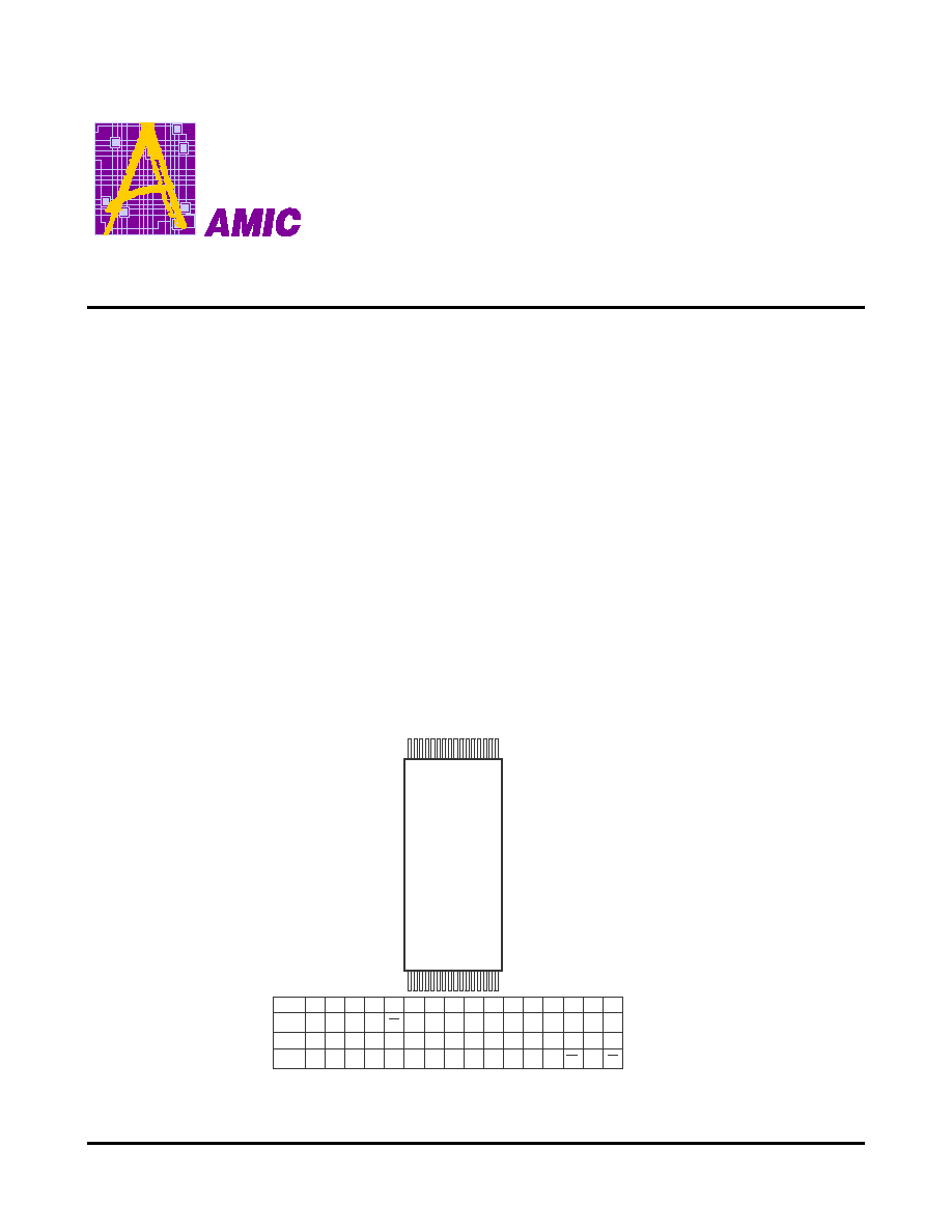
TSOP/TSSOP
LP62S1024AV-I
(LP62S1024AX-I)
1
16
17
32
Pin No.
Pin
Name
Pin No.
Pin
Name
1
2
A9
3
4
5
6
7
8
9
10
11
12
13
14
30
29
28
27
26
25
24
22
19
21
20
23
18
17
A8
A13
CE2
A15
VCC
NC
I/O
8
A16
A14
A12
A7
A6
A3
A2
A1
A0
I/O
1
I/O
2
GND
I/O
4
I/O
5
I/O
6
I/O
7
I/O
3
A11
WE
CE1
15
16
31
32
A5
A4
A10
OE
LP62S1024A-I Series
PRELIMINARY (August, 2001, Version 0.1)
2
AMIC Technology, Inc.
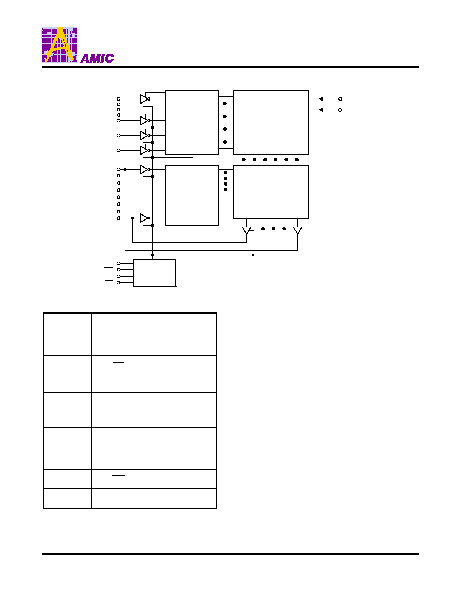
Block Diagram
ROW
DECODER
512 X 2048
MEMORY ARRAY
INPUT DATA
CIRCUIT
COLUMN I/O
CONTROL
CIRCUIT
CE2
CE1
WE
I/O
8
I/O
1
A16
A15
A14
A0
VCC
GND
OE
Pin Description ≠ TSOP/TSSOP
Pin No.
Symbol
Description
1 - 4, 7,
10 - 20, 31
A0 - A16
Address Inputs
5
WE
Write Enable
6
CE2
Chip Enable
8
VCC
Power Supply
9
NC
No Connection
21 - 23,
25 - 29
I/O
1
- I/O
8
Data Input/Outputs
24
GND
Ground
30
CE1
Chip Enable
32
OE
Output Enable
LP62S1024A-I Series
PRELIMINARY (August, 2001, Version 0.1)
3
AMIC Technology, Inc.
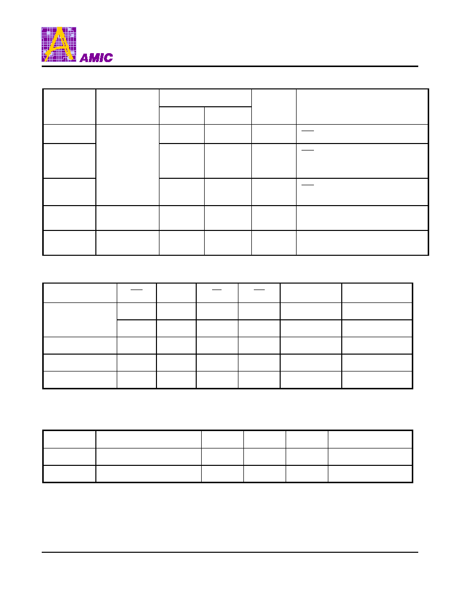
Recommended DC Operating Conditions
(T
A
= -40
∞
C to +85
∞
C)
Symbol
Parameter
Min.
Typ.
Max.
Unit
VCC
Supply Voltage
2.7
3.0
3.6
V
GND
Ground
0
0
0
V
V
IH
Input High Voltage
2.0
-
VCC + 0.3
V
V
IL
Input Low Voltage
-0.3
-
+0.6
V
C
L
Output Load
-
-
30
pF
TTL
Output Load
-
-
1
-
LP62S1024A-I Series
PRELIMINARY (August, 2001, Version 0.1)
4
AMIC Technology, Inc.
Absolute Maximum Ratings*
VCC to GND .............................................. -0.5V to +4.6V
IN, IN/OUT Volt to GND .....................-0.5V to VCC +0.5V
Operating Temperature, Topr ................... -40
∞
C to +85
∞
C
Storage Temperature, Tstg..................... -55
∞
C to +125
∞
C
Temperature Under Bias, Tbias................ -10
∞
C to +85
∞
C
Power Dissipation, P
T
...............................................0.7W
*Comments
Stresses above those listed under "Absolute Maximum
Ratings" may cause permanent damage to this device.
These are stress ratings only. Functional operation of this
device at these or any other conditions above those
indicated in the operational sections of this specification
is not implied or intended. Exposure to the absolute
maximum rating conditions for extended periods may
affect device reliability.
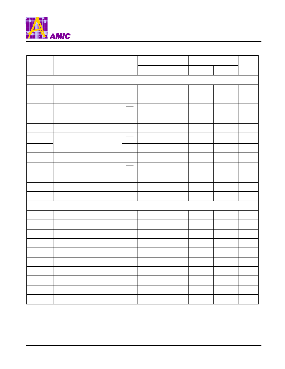
DC Electrical Characteristics
(T
A
= -40
∞
C to +85
∞
C, VCC = 2.7V to 3.6V, GND = 0V)
Symbol
Parameter
LP62S1024A-55LLI/70LLI
Unit
Conditions
Min.
Max.
I
LI
Input Leakage
Current
-
1
µ
A
V
IN
= GND to VCC
I
LO
Output Leakage
Current
-
1
µ
A
CE1 = V
IH
or CE2 = V
IL
V
I/O
= GND to VCC
I
CC
Active Power Supply
Current
-
3
mA
CE1 = V
IL
, CE2 = V
IH
I
I/O
= 0mA
-
-70NS:30
I
CC1
Dynamic Operating
-
-55NS:40
mA
Min. Cycle, Duty = 100%
CE1 = V
IL
, CE2 = V
IH
I
I/O
= 0mA
I
CC2
Current
-
5
mA
CE1 = V
IL
, CE2 = V
IH
f = 1 MH
Z,
I
I/O
= 0mA
LP62S1024A-I Series
PRELIMINARY (August, 2001, Version 0.1)
5
AMIC Technology, Inc.
DC Electrical Characteristics (continued)
Symbol
Parameter
LP62S1024A-55LLI/70LLI
Unit
Conditions
Min.
Max.
I
SB
-
0.5
mA
CE1 = V
IH
or CE2 =V
IL
I
SB1
Standby Power
Supply Current
-
5
µ
A
CE1
VCC - 0.2V , CE2
VCC - 0.2V
V
IN
VCC - 0.2V or V
IN
0.2V
I
SB2
-
5
µ
A
CE1
0.2V , CE2
0.2V
V
IN
VCC - 0.2V or V
IN
0.2V
V
OL
Output Low
Voltage
-
0.4
V
I
OL
= 2.1mA
V
OH
Output High
Voltage
2.2
-
V
I
OH
= -1.0mA
Truth Table
Mode
CE1
CE2
OE
WE
I/O Operation
Supply Current
Standby
H
X
X
X
High Z
I
SB
, I
SB1
X
L
X
X
High Z
I
SB
, I
SB2
Output Disable
L
H
H
H
High Z
I
CC,
I
CC1,
I
CC2
Read
L
H
L
H
D
OUT
I
CC,
I
CC1,
I
CC2
Write
L
H
X
L
D
IN
I
CC,
I
CC1,
I
CC2
Note: X = H or L
Capacitance
(T
A
= 25
∞
C, f = 1.0MHz)
Symbol
Parameter
Min.
Max.
Unit
Conditions
C
IN
*
Input Capacitance
6
pF
V
IN
= 0V
C
I/O
*
Input/Output Capacitance
8
pF
V
I/O
= 0V
* These parameters are sampled and not 100% tested.
LP62S1024A-I Series
PRELIMINARY (August, 2001, Version 0.1)
6
AMIC Technology, Inc.
AC Characteristics
(T
A
= -40
∞
C to +85
∞
C, VCC = 2.7V to 3.6V)
Symbol
Parameter
LP62S1024A-55LLI
LP62S1024A-70LLI
Unit
Min.
Max.
Min.
Max.
Read Cycle
t
RC
Read Cycle Time
55
-
70
-
ns
t
AA
Address Access Time
-
55
-
70
ns
t
ACE1
Chip Enable Access Time
CE1
-
55
-
70
ns
t
ACE2
CE2
-
55
-
70
ns
t
OE
Output Enable to Output Valid
-
30
-
35
ns
t
CLZ1
Chip Enable to Output in Low Z
CE1
10
-
10
-
ns
t
CLZ2
CE2
10
-
10
-
ns
t
OLZ
Output Enable to Output in Low Z
5
-
5
-
ns
t
CHZ1
Chip Disable to Output in High Z
CE1
0
20
0
25
ns
t
CHZ2
CE2
0
20
0
25
ns
t
OHZ
Output Disable to Output in High Z
0
20
0
25
ns
t
OH
Output Hold from Address Change
5
-
10
-
ns
Write Cycle
t
WC
Write Cycle Time
55
-
70
-
ns
t
CW
Chip Enable to End of Write
50
-
60
-
ns
t
AS
Address Setup Time
0
-
0
-
ns
t
AW
Address Valid to End of Write
50
-
60
-
ns
t
WP
Write Pulse Width
40
-
50
-
ns
t
WR
Write Recovery Time
0
-
0
-
ns
t
WHZ
Write to Output in High Z
0
25
0
25
ns
t
DW
Data to Write Time Overlap
25
-
30
-
ns
t
DH
Data Hold from Write Time
0
-
0
-
ns
t
OW
Output Active from End of Write
5
-
5
-
ns
Notes: t
CHZ1
, t
CHZ2
, t
OHZ
, and t
WHZ
are defined as the time at which the outputs achieve the open circuit condition and are
not referred to output voltage levels.
LP62S1024A-I Series
PRELIMINARY (August, 2001, Version 0.1)
7
AMIC Technology, Inc.
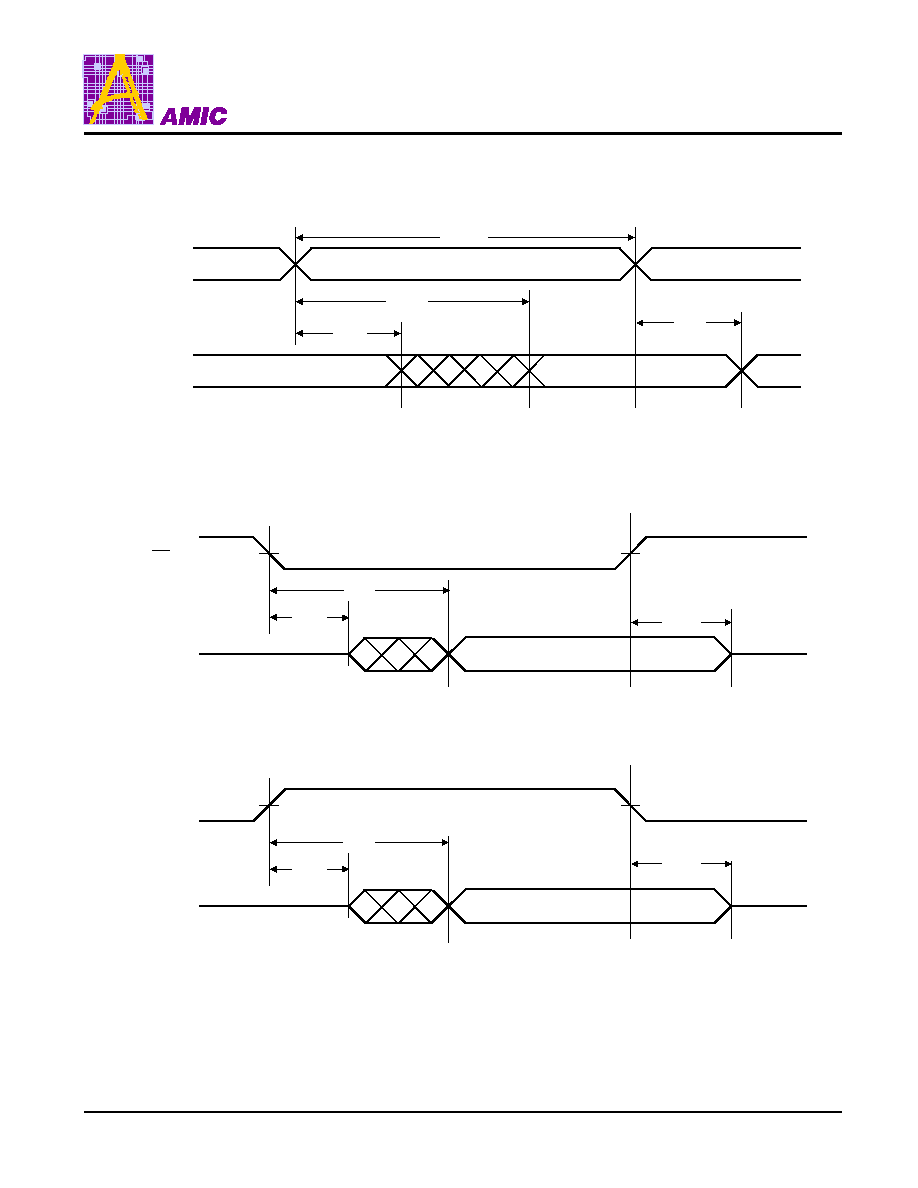
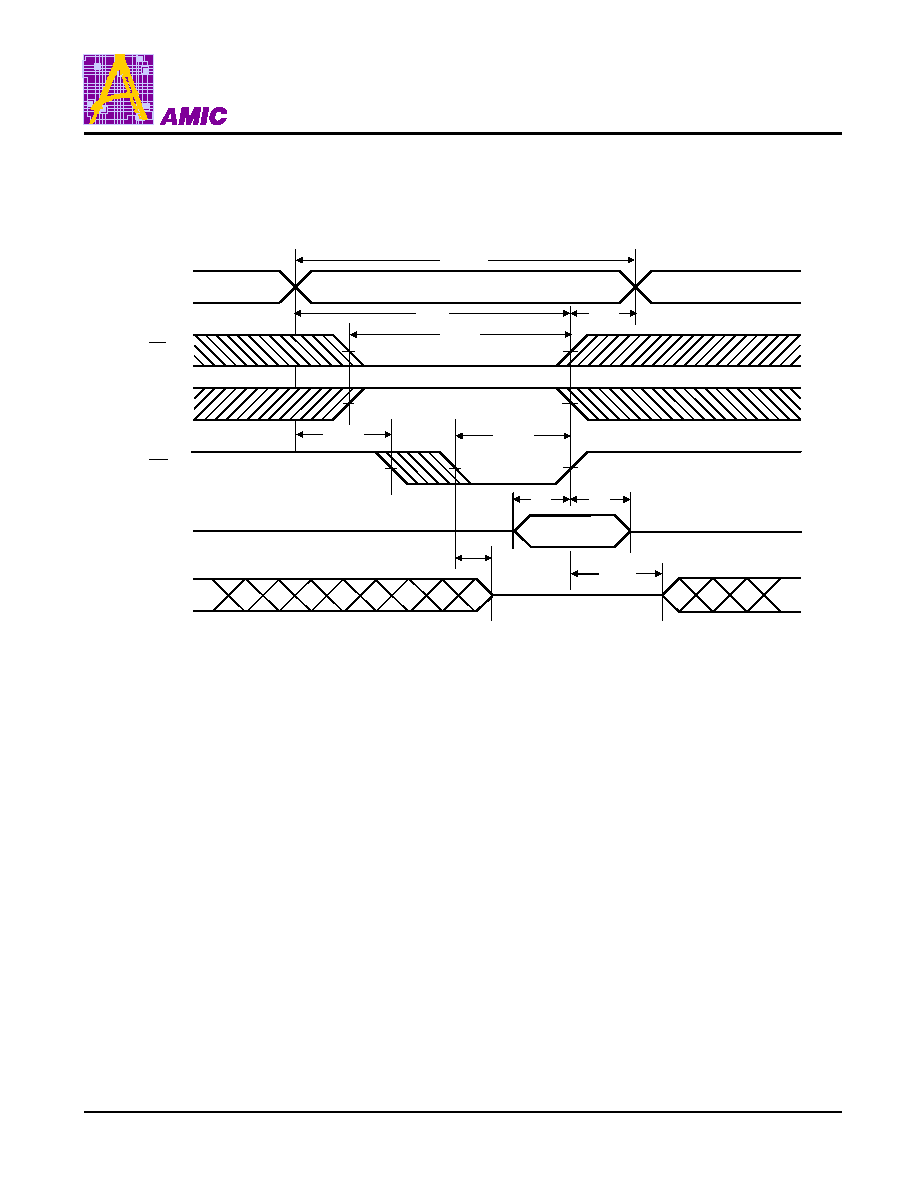
Timing Waveforms
Read Cycle 1
(1, 2, 4)
t
RC
t
OH
t
AA
t
OH
Address
D
OUT
Read Cycle 2
(1, 3, 4, 6)
t
CLZ15
t
ACE1
t
CHZ15
CE1
D
OUT
Read Cycle 3
(1, 4, 7, 8)
t
CLZ25
t
ACE2
t
CHZ25
CE2
D
OUT
LP62S1024A-I Series
PRELIMINARY (August, 2001, Version 0.1)
8
AMIC Technology, Inc.
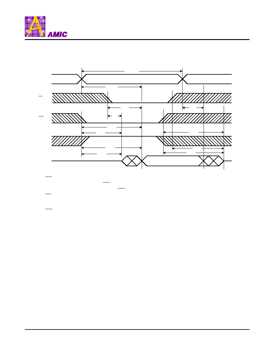
Timing Waveforms (continued)
Read Cycle 4
(1)
t
RC
Address
CE2
D
OUT
t
AA
t
OE
t
OLZ5
t
ACE1
t
CLZ15
t
ACE2
t
CLZ25
t
CHZ25
t
OHZ5
t
CHZ15
t
OH
OE
CE1
Notes: 1. WE is high for Read Cycle.
2. Device is continuously enabled CE1 = V
IL
and CE2 = V
IH
.
3. Address valid prior to or coincident with CE1 transition low.
4. OE = V
IL
.
5. Transition is measured
±
500mV from steady state. This parameter is sampled and not 100% tested.
6. CE2 is high.
7. CE1 is low.
8. Address valid prior to or coincident with CE2 transition high.
LP62S1024A-I Series
PRELIMINARY (August, 2001, Version 0.1)
9
AMIC Technology, Inc.
Timing Waveforms (continued)
Write Cycle 1
(6)
(Write Enable Controlled)
t
WC
Address
CE1
CE2
D
IN
t
OW
t
DH
t
DW
t
WHZ
t
WP2
t
AS1
(4)
t
CW5
t
AW
t
WR3
WE
D
OUT
(4)
LP62S1024A-I Series
PRELIMINARY (August, 2001, Version 0.1)
10
AMIC Technology, Inc.
Timing Waveforms (continued)
Write Cycle 2
(Chip Enable Controlled)
t
WC
Address
CE1
CE2
D
IN
t
DH
t
DW
(4)
(4)
t
CW5
t
AW
t
WR3
WE
D
OUT
t
WHZ7
t
WP2
t
CW5
t
AS1
Notes: 1. t
AS
is measured from the address valid to the beginning of Write.
2. A Write occurs during the overlap (t
WP
) of a low CE1, a high CE2 and a low WE .
3. t
WR
is measured from the earliest of CE1 or WE going high or CE2 going low to the end of the Write cycle.
4. If the CE1 low transition or the CE2 high transition occurs simultaneously with the WE low transition or after
the WE transition, outputs remain in a high impedance state.
5. t
CW
is measured from the later of CE1 going low or CE2 going high to the end of Write.
6. OE is continuously low. ( OE = V
IL
)
7. Transition is measured
±
500mV from steady state. This parameter is sampled and not 100% tested.
LP62S1024A-I Series
PRELIMINARY (August, 2001, Version 0.1)
11
AMIC Technology, Inc.
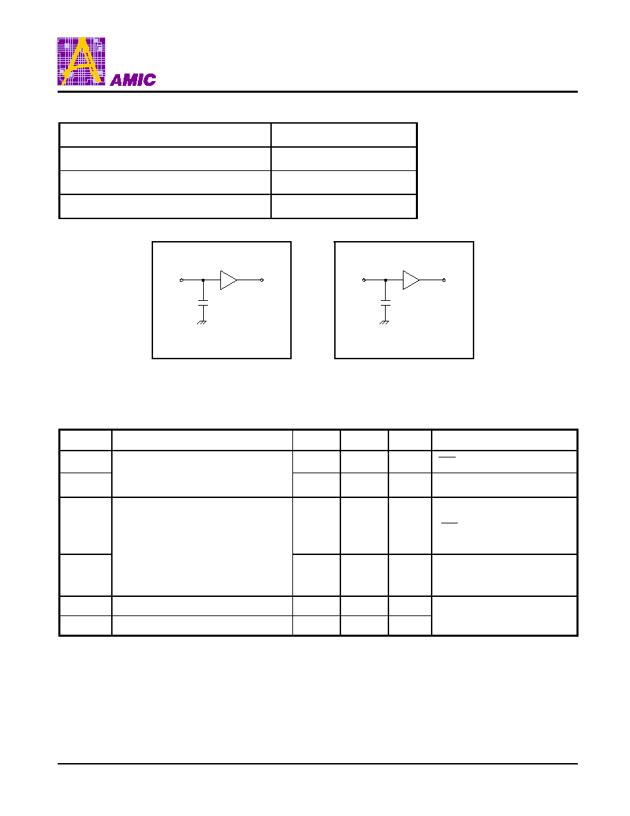
AC Test Conditions
Input Pulse Levels
0.4V to 2.4V
Input Rise and Fall Time
5 ns
Input and Output Timing Reference Levels
1.5V
Output Load
See Figures 1 and 2
30pF
* Including scope and jig.
* Including scope and jig.
C
L
TTL
5pF
C
L
TTL
Figure 1. Output Load
Figure 2. Output Load for t
CLZ1
,
t
CLZ2
, t
OHZ
, t
OLZ
, t
CHZ1
,
t
CHZ2
, t
WHZ
, and t
OW
Data Retention Characteristics
(T
A
= -40
∞
C to 85
∞
C)
Symbol
Parameter
Min.
Max.
Unit
Conditions
V
DR1
2.0
3.6
V
CE1
VCC - 0.2V
V
DR2
VCC for Data Retention
2.0
3.6
V
CE2
0.2V
I
CCDR1
Data Retention Current
-
3*
µ
A
VCC = 2V,
CE1
VCC - 0.2V
V
IN
VCC - 0.2V or V
IN
0.2V
I
CCDR2
-
3*
µ
A
VCC = 2V,
CE2
0.2V
V
IN
VCC - 0.2V or V
IN
0.2V
t
CDR
Chip Disable to Data Retention Time
0
-
ns
See Retention Waveform
t
R
Operation Recovery Time
5
-
ms
* LP62S1024A-55LLI/70LLI
I
CCDR
: max. I
µ
A at T
A
= 0
∞
C to + 40
∞
C
LP62S1024A-I Series
PRELIMINARY (August, 2001, Version 0.1)
12
AMIC Technology, Inc.
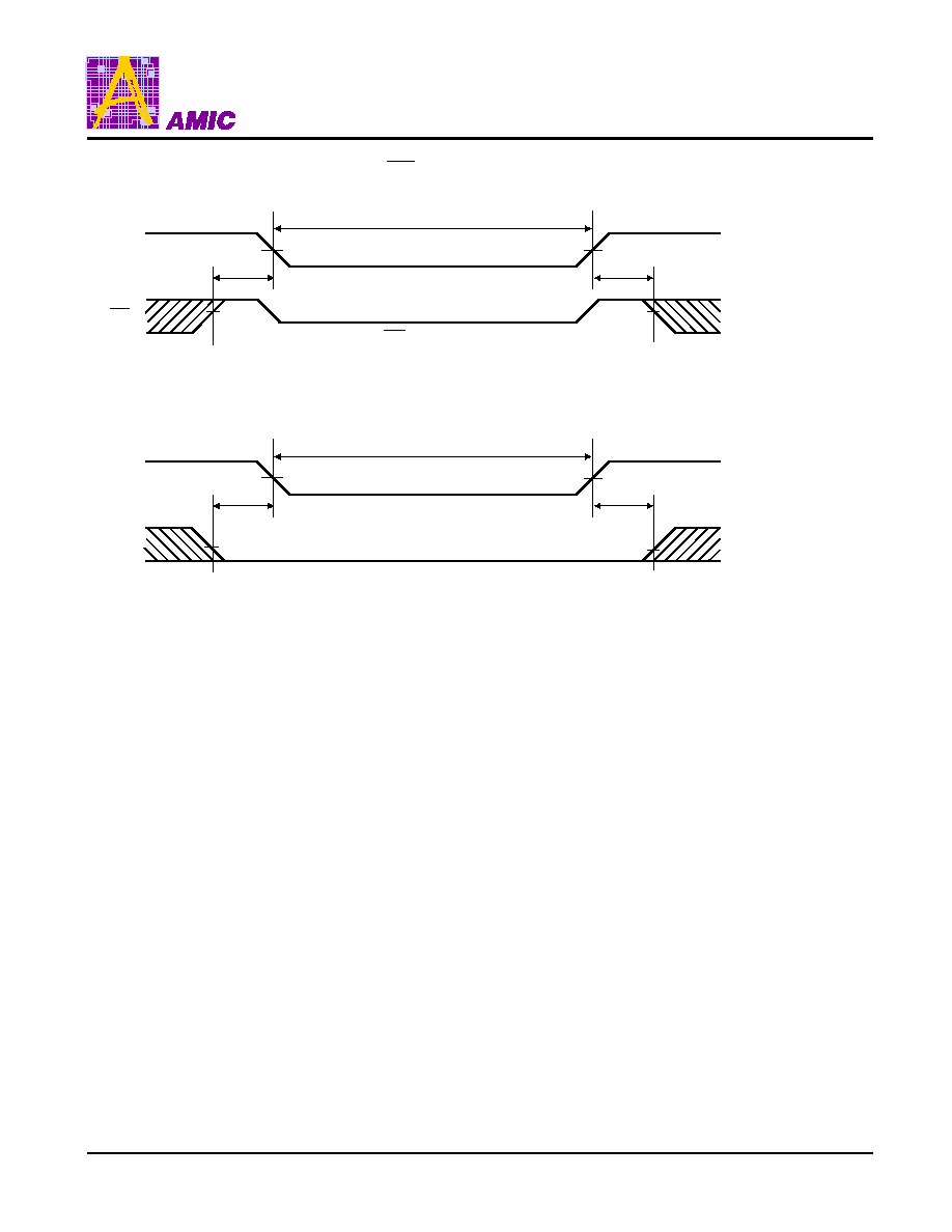
Low VCC Data Retention Waveform (1) ( CE1 Controlled)
VCC
CE1
t
CDR
V
IH
3.0V
t
R
V
IH
3.0V
DATA RETENTION MODE
V
DR
2V
CE1
V
DR
- 0.2V
Low VCC Data Retention Waveform (2) (CE2 Controlled)
VCC
CE2
t
CDR
V
IL
3.0V
t
R
V
IL
3.0V
DATA RETENTION MODE
V
DR
2V
CE2
0.2V
LP62S1024A-I Series
PRELIMINARY (August, 2001, Version 0.1)
13
AMIC Technology, Inc.
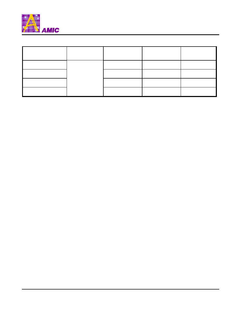
Ordering Information
Part No.
Access Time (ns)
Operating Current
Max. (mA)
Standby Current
Max. (
µ
µ
A)
Package
LP62S1024AV-55LLI
40
5
32L TSOP
LP62S1024AX-55LLI
40
5
32L TSSOP
LP62S1024AV-70LLI
30
5
32L TSOP
LP62S1024AX-70LLI
30
5
32L TSSOP
LP62S1024A-I Series
PRELIMINARY (August, 2001, Version 0.1)
14
AMIC Technology, Inc.
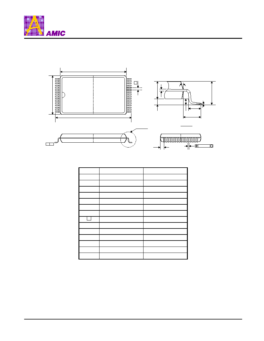
Package Information
TSOP 32L TYPE I (8 X 20mm) Outline Dimensions
unit: inches/mm
e
L
E
L
GAUGE PLANE
A
A
2
c
0.25
BSC
Detail "A"
D y
Detail "A"
S
A
1
b
H
D
D
E
0.10(0.004)
M
∞
12.0
Symbol
Dimensions in inches
Dimensions in mm
A
0.047 Max.
1.20 Max.
A
1
0.004±0.002
0.10±0.05
A
2
0.039±0.002
1.00±0.05
b
0.008±0.001
0.20±0.03
c
0.006±0.001
0.15±0.02
D
0.724±0.004
18.40±0.10
E
0.315±0.004
8.00±0.10
e
0.020 TYP.
0.50 TYP.
H
D
0.787±0.007
20.00±0.20
L
0.020±0.004
0.50±0.10
L
E
0.031 TYP.
0.80 TYP.
S
0.0167 TYP.
0.425 TYP.
Y
0.004 Max.
0.10 Max.
0
∞
~ 6
∞
0
∞
~ 6
∞
Notes:
1. The maximum value of dimension D includes end flash.
2. Dimension E does not include resin fins.
3. Dimension e
1
is for PC Board surface mount pad pitch design
reference only.
4. Dimension S includes end flash.
LP62S1024A-I Series
PRELIMINARY (August, 2001, Version 0.1)
15
AMIC Technology, Inc.
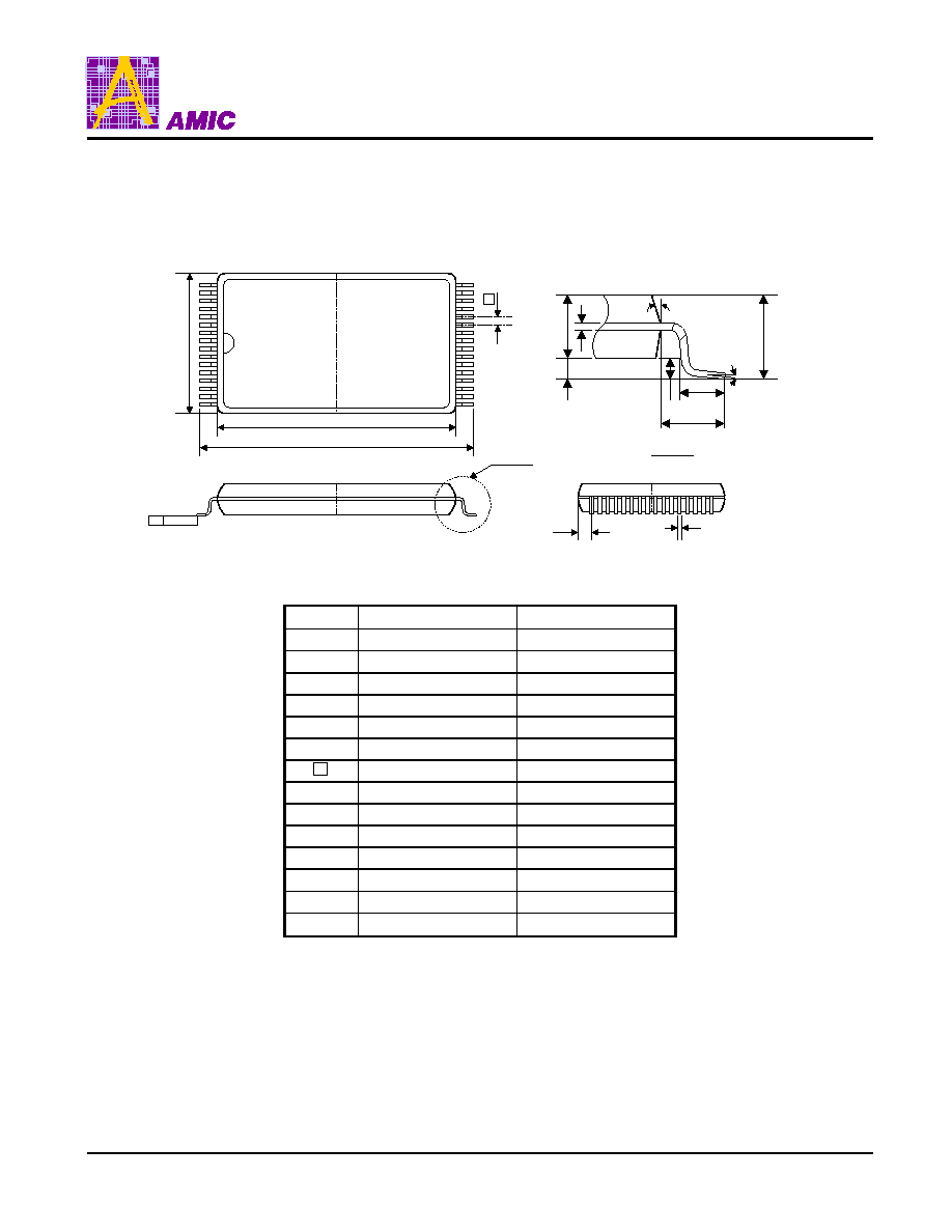
Package Information
TSSOP 32L TYPE I (8 X 13.4mm) Outline Dimensions
unit: inches/mm
e
Detail "A"
D
0.10MM
Detail "A"
S
b
D
1
E
D
L
E
L
GAUGE PLANE
A
A
2
c
0.25
BSC
Detail "A"
A
1
SEATING PLANE
∞
.
0
12
Symbol
Dimensions in inches
Dimensions in mm
A
0.049 Max.
1.25 Max.
A
1
0.002 Min.
0.05 Min.
A
2
0.039±0.002
1.00±0.05
b
0.008±0.001
0.20±0.03
c
0.006±0.0003
0.15±0.008
E
0.315±0.004
8.00±0.10
e
0.020 TYP.
0.50 TYP.
D
0.528±0.008
13.40±0.20
D
1
0.465±0.004
11.80±0.10
L
0.02±0.008
0.50±0.20
L
E
0.0266 Min.
0.675 Min.
S
0.0109 TYP.
0.278 TYP.
y
0.004 Max.
0.10 Max.
0
∞
~ 6
∞
0
∞
~ 6
∞
Notes:
1. The maximum value of dimension D includes end flash.
2. Dimension E does not include resin fins.
3. Dimension e
1
is for PC Board surface mount pad pitch design
reference only.
4. Dimension S includes end flash.