
LP62S16256E-T Series
256K X 16 BIT LOW VOLTAGE CMOS SRAM
(January, 2002, Version 2.0)
AMIC Technology, Inc.
Document Title
256K X 16 BIT LOW VOLTAGE CMOS SRAM
Revision History
Rev. No. History
Issue Date
Remark
2.0
Change V
CC
max
from 3.3V to 3.6V
January 25, 2002
Add product family and 55ns specification
LP62S16256E-T Series
256K X 16 BIT LOW VOLTAGE CMOS SRAM
(January, 2002, Version 2.0)
2
AMIC Technology, Inc.
Features
n
Operating voltage: 2.7V to 3.6V
n
Access times: 55ns / 70ns (max.)
n
Current:
Very low power version: Operating: 40mA (max.)
Standby:
10
�
A (max.)
n
Full static operation, no clock or refreshing required
n
All inputs and outputs are directly TTL-compatible
n
Common I/O using three-state output
n
Data retention voltage: 2.0V (min.)
n
Available in 44-pin TSOP and 48-ball CSP (6
�
8mm)
packages
General Description
The LP62S16256E-T is a low operating current 4,194,304-
bit static random access memory organized as 262,144
words by 16 bits and operates on low power voltage from
2.7V to 3.3V. It is built using AMIC's high performance
CMOS process.
Inputs and three-state outputs are TTL compatible and
allow for direct interfacing with common system bus
structures.
The chip enable input is provided for POWER-DOWN,
device enable. Two byte enable inputs and an output
enable input are included for easy interfacing.
Data retention is guaranteed at a power supply voltage as
low as 2.0V.
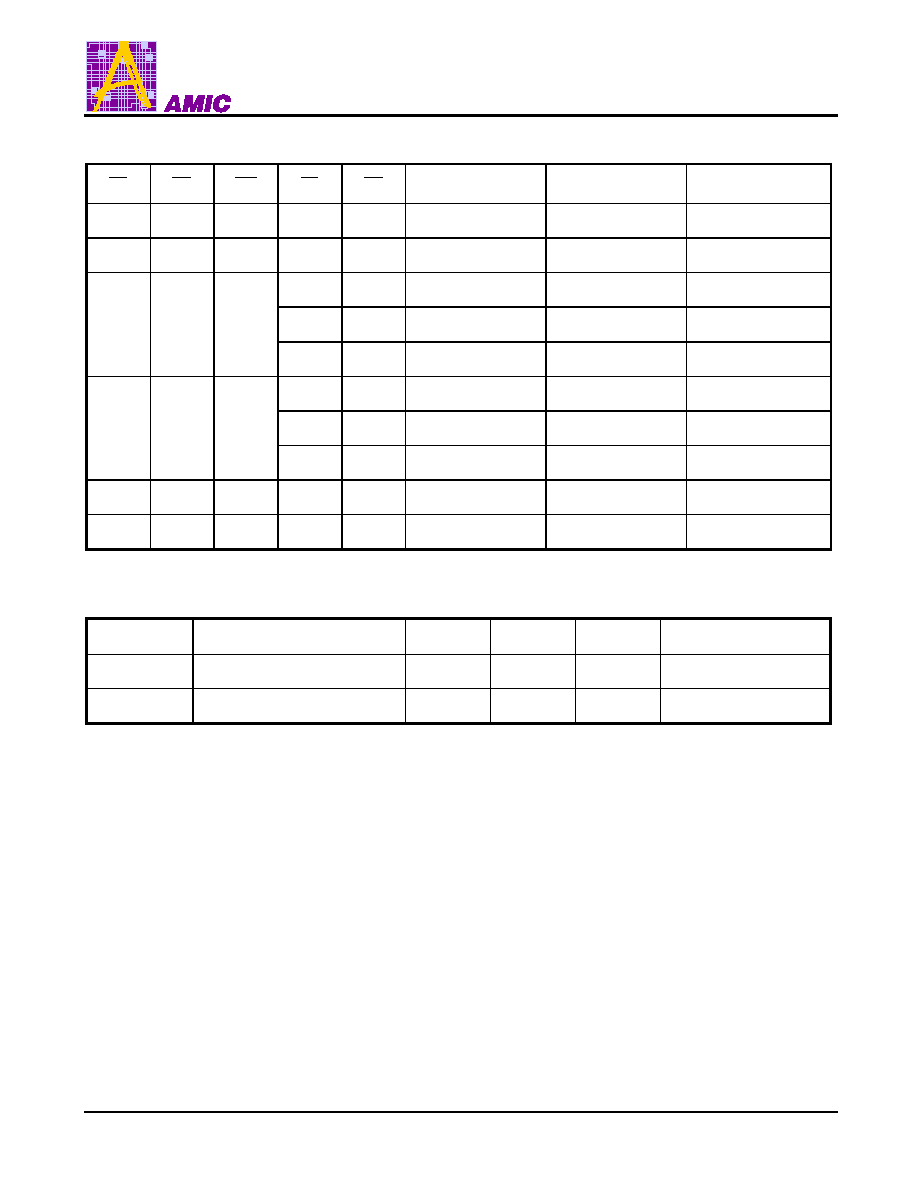
Product Family
Power Dissipation
Product Family
Operating
Temperature
VCC
Range
Speed
Data Retention
(I
CCDR
, Typ.)
Standby
(I
SB1
, Typ.)
Operating
(I
CC2
, Typ.)
Package
Type
LP62S16256E-T
-25
�
C ~ +85
�
C
2.7V~3.6V
55ns / 70ns
0.08
�
A
0.3
�
A
5mA
44L TSOP
48B CSP
1. Typical values are measured at VCC = 3.0V, T
A
= 25
�
C and not 100% tested.
2. Data retention current VCC = 2.0V.
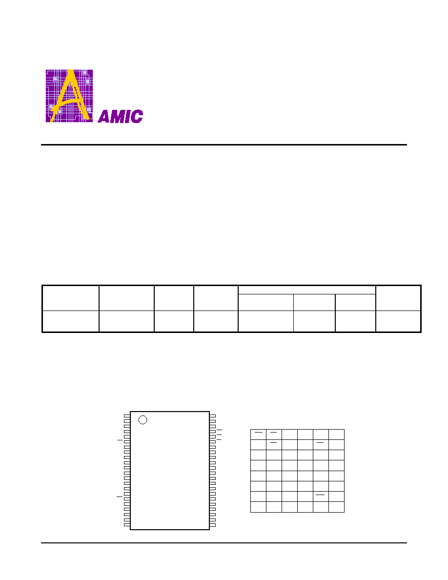
Pin Configurations
n
n
TSOP
n
n
CSP (Chip Size Package)
48-pin Top View
I/O
9
I/O
10
GND
VCC
I/O
15
I/O
16
NC
A8
NC
A9
A12
A10
A11
NC
A13
A14
A15
I/O
8
I/O
7
I/O
3
I/O
1
GND
VCC
A0
A3
A5
A6
A4
A1
A2
NC
6
5
4
3
2
1
A
B
C
D
E
F
G
H
I/O
14
I/O
13
I/O
12
I/O
11
A17
NC
A7
A16
I/O
2
I/O
4
I/O
5
I/O
6
LB
HB
WE
OE
CE
1
2
3
4
5
6
7
8
9
10
11
12
13
14
15
16
17
18
19
20
21
22
A3
A2
A1
A0
CE
I/O
1
I/O
2
I/O
3
I/O
4
VCC
GND
I/O
5
I/O
6
I/O
7
I/O
8
WE
A17
A16
A15
A14
44
43
42
41
40
39
38
37
36
35
34
33
32
31
30
29
28
27
26
25
24
23
A11
A10
A9
A8
NC
I/O
9
I/O
10
I/O
11
I/O
12
VCC
GND
I/O
13
I/O
14
I/O
15
I/O
16
LB
HB
OE
A7
A6
LP62S16256EV-T
A13
A5
A4
A12
LP62S16256E-T Series
(January, 2002, Version 2.0)
3
AMIC Technology, Inc.
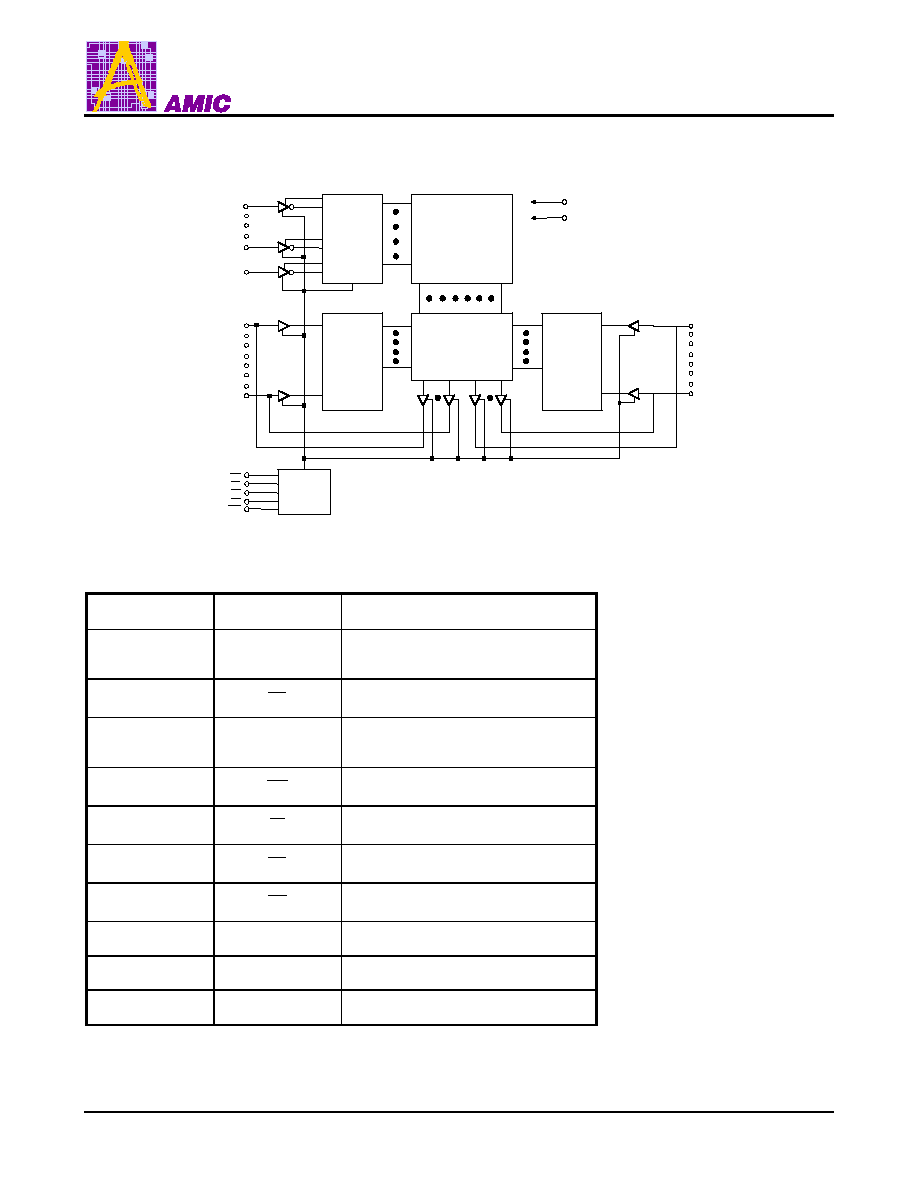
Block Diagram
DECODER
512 X 8192
MEMORY ARRAY
COLUMN I/O
INPUT
DATA
CIRCUIT
CONTROL
CIRCUIT
VCC
GND
I/O
8
I/O
1
A17
A16
A0
WE
HB
INPUT
DATA
CIRCUIT
I/O
9
I/O
16
LB
OE
CE
Pin Descriptions -- TSOP
Pin No.
Symbol
Description
1 - 5, 18 - 27,
42 - 44
A0 - A17
Address Inputs
6
CE
Chip Enable Input
7 - 10, 13 - 16,
29 - 32, 35 - 38
I/O
1
- I/O
16
Data Inputs/Outputs
17
WE
Write Enable Input
39
LB
Lower Byte Enable Input (I/O
1
to I/O
8
)
40
HB
Higher Byte Enable Input (I/O
9
to I/O
16
)
41
OE
Output Enable Input
11, 33
VCC
Power
12, 34
GND
Ground
28
NC
No Connection
LP62S16256E-T Series
(January, 2002, Version 2.0)
4
AMIC Technology, Inc.
Pin Description - CSP
Symbol
Description
Symbol
Description
A0 - A17
Address Inputs
HB
Higher Byte Enable Input
(I/O
9
- I/O
16
)
CE
Chip Enable
OE
Output Enable
I/O
1
- I/O
16
Data Input/Output
VCC
Power Supply
WE
Write Enable Input
GND
Ground
LB
Byte Enable Input
(I/O
1
- I/O
8
)
NC
No Connection
Recommended DC Operating Conditions
(T
A
= -25
�
C to + 85
�
C)
Symbol
Parameter
Min.
Typ.
Max.
Unit
VCC
Supply Voltage
2.7
3
3.6
V
GND
Ground
0
0
0
V
V
IH
Input High Voltage
2.2
-
VCC + 0.3
V
V
IL
Input Low Voltage
-0.3
-
+0.6
V
C
L
Output Load
-
-
30
pF
TTL
Output Load
-
-
1
-
LP62S16256E-T Series
(January, 2002, Version 2.0)
5
AMIC Technology, Inc.
Absolute Maximum Ratings*
VCC to GND ..............................................-0.5V to +4.0V
IN, IN/OUT Volt to GND ................... -0.5V to VCC + 0.5V
Operating Temperature, Topr ...................-25
�
C to +85
�
C
Storage Temperature, Tstg.....................-55
�
C to +125
�
C
Power Dissipation, P
T ......................................................................
0.7W
*Comments
Stresses above those listed under "Absolute Maximum
Ratings" may cause permanent damage to this device.
These are stress ratings only. Functional operation of this
device at these or any other conditions above those
indicated in the operational sections of this specification
is not implied or intended. Exposure to the absolute
maximum rating conditions for extended periods may
affect device reliability.
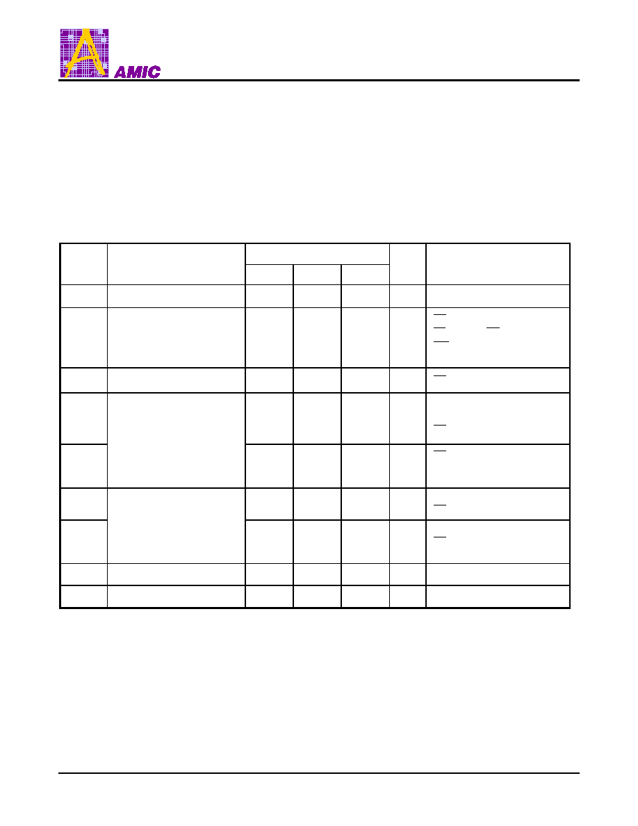
DC Electrical Characteristics
(T
A
= -25
�
C to + 85
�
C, VCC = 2.7V to 3.6V, GND = 0V)
Symbol
Parameter
LP62S16256E-55LLT / 70LLT
Unit
Conditions
Min.
Typ.
Max.
I
LI
Input Leakage Current
-
-
1
�
A
V
IN
= GND to VCC
I
LO
Output Leakage Current
-
-
1
�
A
CE = V
IH
HB = V
IH
or OE = V
IH
or
WE = V
IH
V
I/O
= GND to VCC
I
CC
Active Power Supply Current
-
-
5
mA
CE = V
IL
, I
I/O
= 0mA
I
CC1
-
25
40
mA
Min. Cycle, Duty = 100%
Dynamic Operating
CE = V
I
, I
I/O
= 0mA
I
CC2
Current
-
5
15
mA
CE = V
IL
, V
IH
= VCC,
V
IL
= 0V, f = 1MHz,
I
I/O
= 0 mA
I
SB
-
-
1
mA
VCC
3.3V
CE = V
IH
I
SB1
Standby Current
-
0.3
10
�
A
VCC
3.3V
CE
VCC - 0.2V,
V
IN
0V
V
OL
Output Low Voltage
-
-
0.4
V
I
OL
= 2.1 mA
V
OH
Output High Voltage
2.2
-
-
V
I
OH
= -1.0 mA
LP62S16256E-T Series
(January, 2002, Version 2.0)
6
AMIC Technology, Inc.
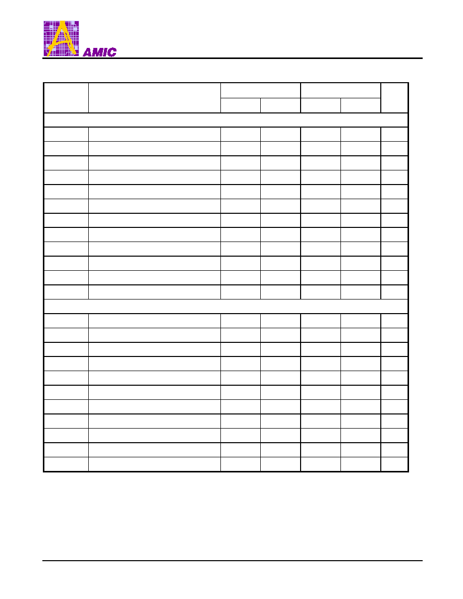
Truth Table
CE
OE
WE
LB
HB
I/O
1
to I/O
8
Mode
I/O
9
to I/O
16
Mode
VCC Current
H
X
X
X
X
Not selected
Not selected
I
SB1
, I
SB
X
X
X
H
H
High - Z
High - Z
I
SB1
, I
SB
L
L
Read
Read
I
CC1
, I
CC2
, I
CC
L
L
H
L
H
Read
High - Z
I
CC1
, I
CC2
, I
CC
H
L
High - Z
Read
I
CC1
, I
CC2
, I
CC
L
L
Write
Write
I
CC1
, I
CC2
, I
CC
L
X
L
L
H
Write
High - Z
I
CC1
, I
CC2
, I
CC
H
L
High - Z
Write
I
CC1
, I
CC2
, I
CC
L
H
H
L
X
High - Z
High - Z
I
CC1
, I
CC2
, I
CC
L
H
H
X
L
High - Z
High - Z
I
CC1
, I
CC2
, I
CC
Note: X = H or L
Capacitance
(T
A
= 25
�
C, f = 1.0MHz)
Symbol
Parameter
Min.
Max.
Unit
Conditions
C
IN
*
Input Capacitance
6
pF
V
IN
= 0V
C
I/O
*
Input/Output Capacitance
8
pF
V
I/O
= 0V
* These parameters are sampled and not 100% tested.
LP62S16256E-T Series
(January, 2002, Version 2.0)
7
AMIC Technology, Inc.
AC Characteristics
(T
A
= -25
�
C to +85
�
C, VCC = 2.7V to 3.6V)
Symbol
Parameter
LP62S16256E-55LLT
LP62S16256E-70LLT
Unit
Min.
Max.
Min.
Max.
Read Cycle
t
RC
Read Cycle Time
55
-
70
-
ns
t
AA
Address Access Time
-
55
-
70
ns
t
ACE
Chip Enable Access Time
-
55
-
70
ns
t
BE
Byte Enable Access Time
-
55
-
70
ns
t
OE
Output Enable to Output Valid
-
30
-
35
ns
t
CLZ
Chip Enable to Output in Low Z
10
-
10
-
ns
t
BLZ
Byte Enable to Output in Low Z
10
-
10
-
ns
t
OLZ
Output Enable to Output in Low Z
5
-
5
-
ns
t
CHZ
Chip Disable to Output in High Z
-
20
-
25
ns
t
BHZ
Byte Disable to Output in High Z
-
20
-
25
ns
t
OHZ
Output Disable to Output in High Z
-
20
-
25
ns
t
OH
Output Hold from Address Change
5
-
5
-
ns
Write Cycle
t
WC
Write Cycle Time
55
-
70
-
ns
t
CW
Chip Enable to End of Write
50
-
60
-
ns
t
BW
Byte Enable to End of Write
50
-
60
-
ns
t
AS
Address Setup Time
0
-
0
-
ns
t
AW
Address Valid to End of Write
50
-
60
-
ns
t
WP
Write Pulse Width
40
-
50
-
ns
t
WR
Write Recovery Time
0
-
0
-
ns
t
WHZ
Write to Output in High Z
-
25
-
25
ns
t
DW
Data to Write Time Overlap
25
-
30
-
ns
t
DH
Data Hold from Write Time
0
-
0
-
ns
t
OW
Output Active from End of Write
5
-
5
-
ns
Note: t
CHZ
, t
BHZ
and t
OHZ
and t
WHZ
are defined as the time at which the outputs achieve the open circuit condition and are
not referred to output voltage levels.
LP62S16256E-T Series
(January, 2002, Version 2.0)
8
AMIC Technology, Inc.
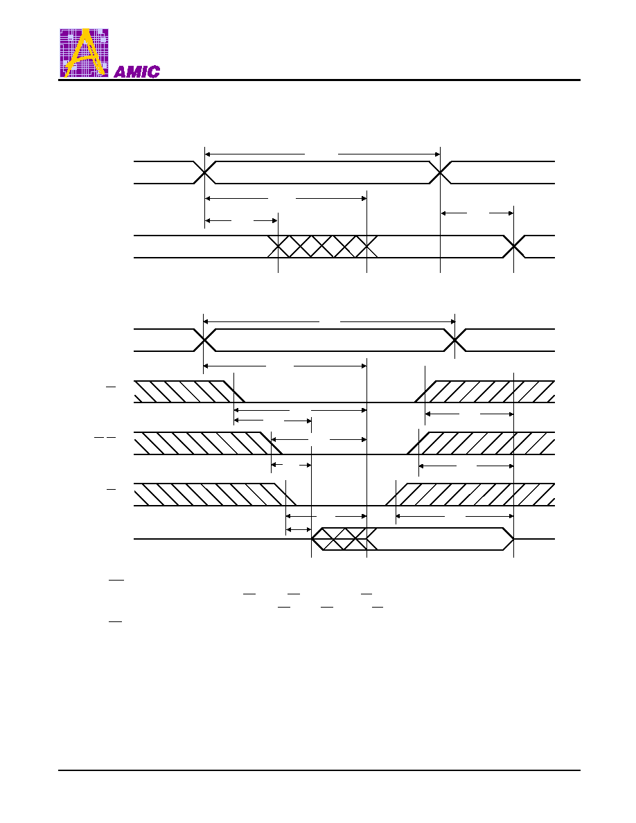
Timing Waveforms
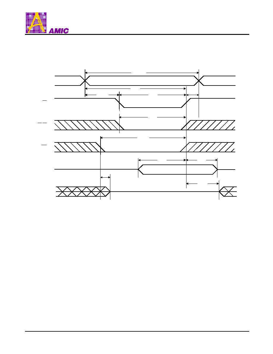
Read Cycle 1
(1, 2, 4)
t
RC
t
OH
t
AA
t
OH
Address
D
OUT
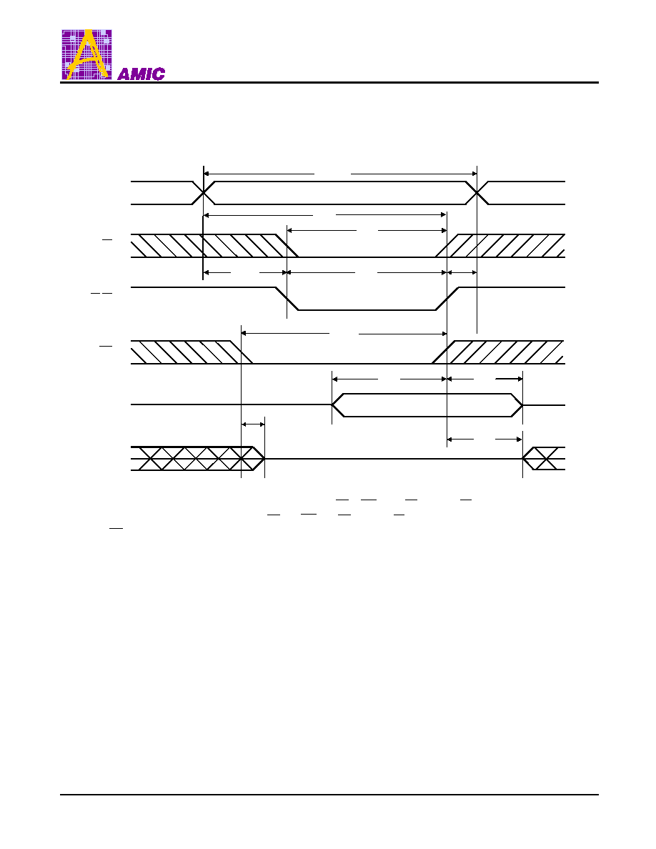
Read Cycle 2
(1, 2, 3)
t
RC
t
AA
Address
t
ACE
t
CHZ5
CE
HB, LB
t
BHZ5
OE
t
CLZ5
t
BE
t
BLZ5
t
OE
t
OLZ5
t
OHZ5
D
OUT
Notes: 1. WE is high for Read Cycle.
2. Device is continuously enabled CE = V
IL
, HB = V
IL
and, or LB = V
IL
.
3. Address valid prior to or coincident with CE and ( HB and, or LB ) transition low.
4. OE = V
IL
.
5. Transition is measured
�
500mV from steady state. This parameter is sampled and not 100% tested.
LP62S16256E-T Series
(January, 2002, Version 2.0)
9
AMIC Technology, Inc.
Timing Waveforms (continued)
Write Cycle 1
(Write Enable Controlled)
t
WC
t
AW
Address
DATA IN
DATA OUT
WE
HB, LB
CE
t
WR3
t
CW
t
BW
t
AS1
t
WP2
t
DW
t
DH
t
OW
t
WHZ4
LP62S16256E-T Series
(January, 2002, Version 2.0)
10
AMIC Technology, Inc.
Timing Waveforms (continued)
Write Cycle 2
(Chip Enable Controlled)
t
WC
t
AW
Address
DATA IN
DATA OUT
WE
HB, LB
CE
t
WR3
t
CW2
t
BW
t
AS1
t
WP
t
DW
t
DH
t
OW
t
WHZ4
LP62S16256E-T Series
(January, 2002, Version 2.0)
11
AMIC Technology, Inc.
Timing Waveforms (continued)
Write Cycle 3
(Byte Enable Controlled)
t
WC
t
AW
Address
DATA IN
DATA OUT
WE
HB, LB
CE
t
WR3
t
CW
t
BW2
t
AS1
t
WP
t
DW
t
DH
t
OW
t
WHZ4
Notes: 1. t
AS
is measured from the address valid to the beginning of Write.
2. A Write occurs during the overlap (t
WP
, t
BW
) of a low CE , WE and ( HB and , or LB ).
3. t
WR
is measured from the earliest of CE or WE or ( HB and , or LB ) going high to the end of the Write cycle.
4. OE level is high or low.
5. Transition is measured
�
500mV from steady state. This parameter is sampled and not 100% tested.
LP62S16256E-T Series
(January, 2002, Version 2.0)
12
AMIC Technology, Inc.
AC Test Conditions
Input Pulse Levels
0.4V to 2.4V
Input Rise And Fall Time
5 ns
Input and Output Timing Reference Levels
1.5V
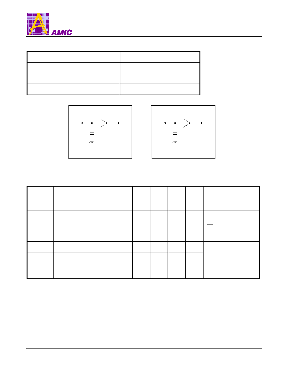
Output Load
See Figures 1 and 2
30pF
* Including scope and jig.
* Including scope and jig.
C
L
TTL
5pF
C
L
TTL
Figure 1. Output Load
Figure 2. Output Load for t
CLZ
,
t
OLZ
,
t
CHZ
,
t
OHZ
,
t
WHZ
,
and t
OW
Data Retention Characteristics
(T
A
= -25
�
C to 85
�
C)
Symbol
Parameter
Min.
Typ.
Max.
Unit
Conditions
V
DR
VCC for Data Retention
2.0
-
3.6
V
CE
VCC - 0.2V
I
CCDR
Data Retention Current
-
0.08
3*
�
A
VCC = 2.0V,
CE
VCC - 0.2V
V
IN
0V
t
CDR
Chip Disable to Data Retention Time
0
-
-
ns
t
R
Operation Recovery Time
t
RC
-
-
ns
See Retention Waveform
t
VR
VCC Rising Time from Data Retention
Voltage to Operating Voltage
5
-
-
ms
* LP62S16256E-55LLT / 70LLT
I
CCDR
: max. 1
�
A at T
A
= 0
�
C to + 40
�
C
LP62S16256E-T Series
(January, 2002, Version 2.0)
13
AMIC Technology, Inc.
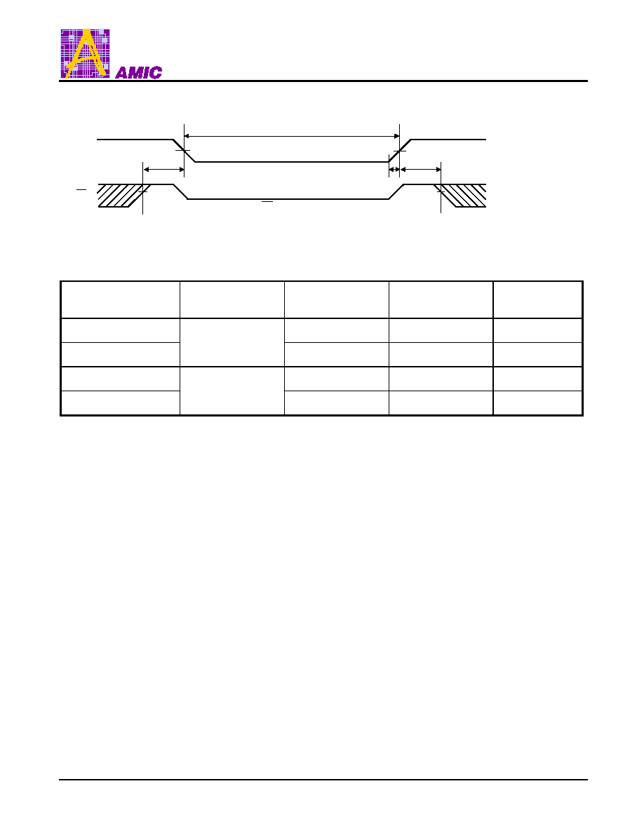
Low VCC Data Retention Waveform
VCC
CE
t
CDR
V
IH
2.7V
t
R
V
IH
2.7V
DATA RETENTION MODE
t
VR
V
DR
2.0V
CE
V
DR
- 0.2V
Ordering Information
Part No.
Access Time (ns)
Operating Current
Max. (mA)
Standby Current
Max. (
�
�
A)
Package
LP62S16256EV-55LLT
55
40
10
44L TSOP
LP62S16256EU-55LLT
40
10
48L CSP
LP62S16256EV-70LLT
70
40
10
44L TSOP
LP62S16256EU-70LLT
40
10
48L CSP
LP62S16256E-T Series
(January, 2002, Version 2.0)
14
AMIC Technology, Inc.
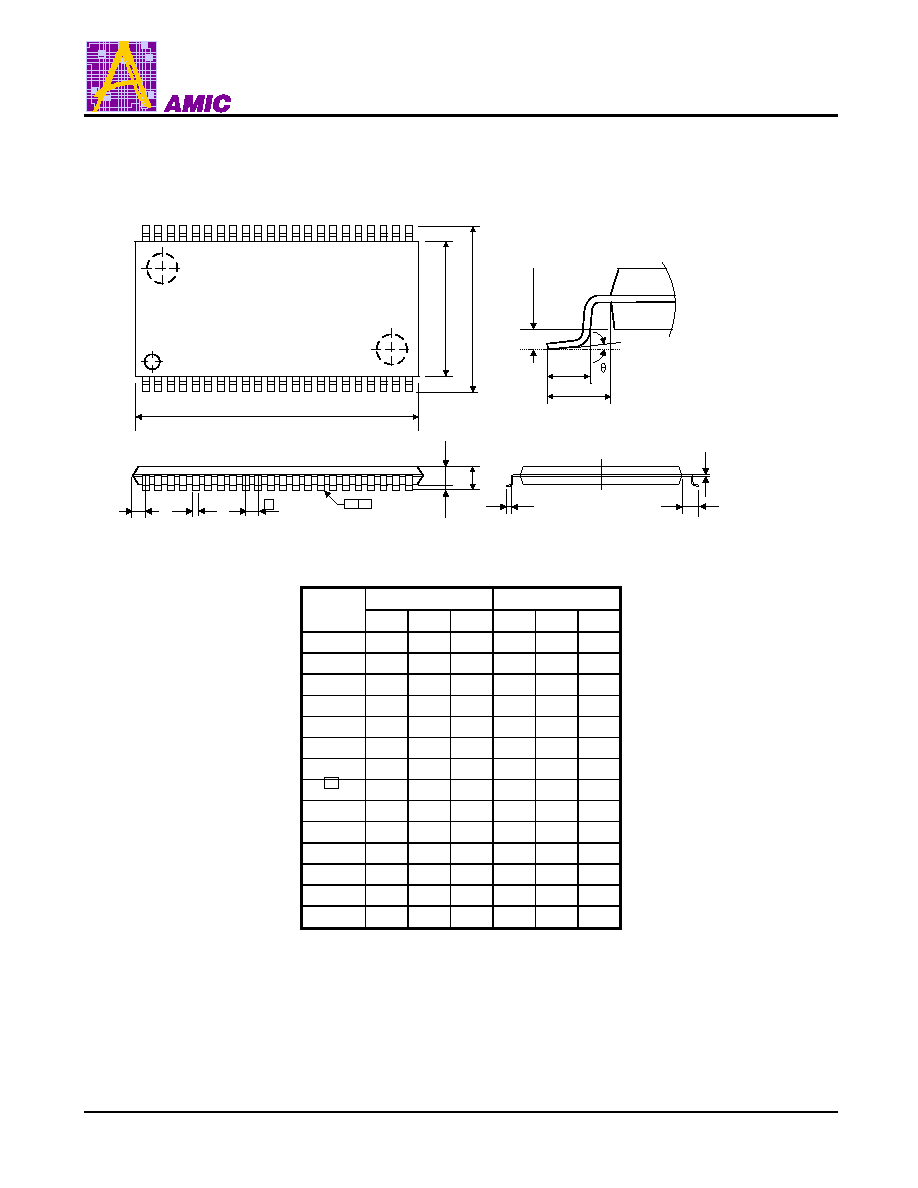
Package Information
TSOP 44L TYPE II Outline Dimensions
unit: inches/mm
44
1
D
E
H
E
0.254
L
1
L
A
1
A
2
A
S
B
e
D y
L
1
c
L
23
22
Symbol
Dimension in inch
Dimension in mm
Min. Nom. Max. Min. Nom. Max.
A
-
-
0.047
-
-
1.20
A
1
0.002
-
-
0.05
-
-
A
2
0.037 0.039 0.041 0.95
1.00
1.05
B
0.010 0.014 0.018 0.25
0.35
0.45
c
-
0.006
-
-
0.15
-
D
0.721 0.725 0.729 18.31 18.41 18.51
E
0.396 0.400 0.404 10.06 10.16 10.26
e
-
0.031
-
-
0.80
-
H
E
0.455 0.463 0.471 11.56 11.76 11.96
L
0.016 0.020 0.024 0.40
0.50
0.60
L
1
-
0.031
-
-
0.80
-
S
-
-
0.036
-
-
0.93
y
-
-
0.004
-
-
0.10
0
�
-
5
�
0
�
-
5
�
Notes:
1. Dimension D&E do not include interlead flash.
2. Dimension B does not include dambar protrusion/intrusion.
3. Dimension S includes end flash.
LP62S16256E-T Series
(January, 2002, Version 2.0)
15
AMIC Technology, Inc.
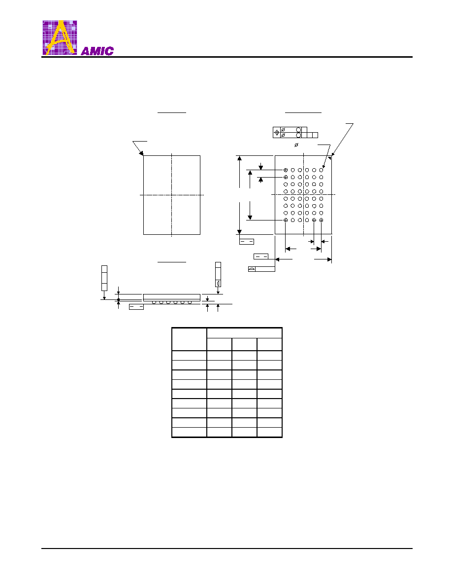
Package Information
48LD CSP ( 6 x 8 mm ) Outline Dimensions
unit: mm
(48TFBGA)
A
1
A
2
A
B
C
D
E
F
G
H
TOP VIEW
Ball#A1 CORNER
SIDE VIEW
C
SEATING PLANE
//
0.25
C
A
(0.36)
A
B
C
D
E
F
G
H
1 2 3 4 5 6
1
2
3
4
5
6
C
0.10
C
S
0.25
S
A B
b (48X)
BOTTOM VIEW
Ball*A1 CORNER
E
E
1
e
B
e
D
1
D
A
0.20(4X)
0.10
C
Dimensions in mm
Symbol
MIN.
NOM. MAX.
A
1.04
1.14
1.24
A
1
0.20
0.25
0.30
A
2
0.48
0.53
0.58
D
5.90
6.00
6.10
E
7.90
8.00
8.10
D
1
---
3.75
---
E
1
---
5.25
---
e
---
0.75
---
b
0.30
0.35
0.40
Note:
1. THE BALL DIAMETER, BALL PITCH, STAND-OFF & PACKAGE THICKNESS
ARE DIFFERENT FROM JEDEC SPEC MO192 (LOW PROFILE BGA FAMILY).
2. PRIMARY DATUM C AND SEATING PLANE ARE DEFINED BY THE SPHERICAL
CROWNS OF THE SOLDER BALLS.
3. DIMENSION b IS MEASURED AT THE MAXIMUM.
THERE SHALL BE A MINIMUM CLEARANCE OF 0.25mm BETWEEN THE EDGE OF
THE SOLDER BALL AND THE BODY EDGE.
4. BALL PAD OPENING OF SUBSTRATE IS
0.3mm (SMD)
SUGGEST TO DESIGN THE PCB LAND SIZE AS
0.3mm (NSMD)