 | –≠–ª–µ–∫—Ç—Ä–æ–Ω–Ω—ã–π –∫–æ–º–ø–æ–Ω–µ–Ω—Ç: AS1505-T | –°–∫–∞—á–∞—Ç—å:  PDF PDF  ZIP ZIP |

AS1504, AS1505
Octal 8-Bit Programmable Low-Power DACs with
Shutdown and Mid-Scale Reset
austria
micro
systems
D a ta S h e e t
www.austriamicrosystems.com
Revision 1.0
1 - 17
1 General Description
The AS1504/AS1505 are low-power (5µA @ 5V) individ-
ually programmable 8-channel, 8-bit resolution digital-to-
analog converters. All eight DACs share a common ref-
erence-voltage input making them ideal for applications
where adjustments start at a nominal voltage.
The devices feature a low-power shutdown reference
input current (5µA) that enables the devices to maintain
individual DAC latch settings during shutdown until nor-
mal operation is resumed.
The devices are controlled via a standard 3-wire serial
interface. Data is shifted into the DACs via the internal
serial-to-parallel shift register.
The AS1504/AS1505 are available in a 16-pin SOIC-150
package.
Figure 1. Block Diagram
2 Key Features
!
8 Individually-Controlled DACs
!
Replaces 8 Potentiometers
!
Standard 3-Wire Serial Interface
!
Single-Supply Operation: +3 to +5V
!
Mid-Scale Reset Pin (AS1504)
!
Separate V
REFL
Range Setting (AS1505)
!
Shutdown Mode:
25µW (I
DD
and I
REF
)
!
Power-On Reset
!
16-pin SOIC-150 Package
3 Applications
The devices are ideal for video amplifier gain control,
video equipment voltage-controlled frequencies and
bandwidths, CRT display geometric corrections and
automatic adjustments, or any other space-limited DAC
application with low power-consumption requirements.
Table 1. Standard Products
Model
Functionality
AS1504
Mid-Scale Reset Pin
AS1505
Separate V
REFL
Range Settings
DAC
Select
DAC1
GND
V
DD
SDI
CLK
CSN
AS1504 Only
SHDNN
V
REFH
V
REFL
V
OUT
V
REFL
V
REFH
OUT1
DAC8
V
REFH
V
REFL
V
OUT
OUT8
Address
11-Bit
Serial Latch
CK
RSN
D
AS1504/
AS1505
8
8-Bit
Latch
CK
RSN
1
8
8-Bit
Latch
CK RSN
3
8
8
AS1505 Only
RSN
www.austriamicrosystems.com
Revision 1.0
2 - 17
AS1504, AS1505
austria
micro
systems
Data Sheet
4 Absolute Maximum Ratings
Stresses beyond those listed in
Table 2
may cause permanent damage to the device. These are stress ratings only,
and functional operation of the device at these or any other conditions beyond those indicated in
Electrical Character-
istics on page 3
is not implied. Exposure to absolute maximum rating conditions for extended periods may affect
device reliability.
Table 2. Absolute Maximum Ratings
Parameter
Min
Max
Units
Comments
V
DD
to GND
-0.3
+7
V
V
REFH
and V
REFH
to GND
0
V
DD
V
OUTx to GND
0
V
DD
V
Digital Input Voltage to GND
0
V
DD
V
Package Power Dissipation
T
J
Max - T
AMB
/
JA
Operating Temperature Range
-40
+85
∫C
Storage Temperature Range
-65
+150
∫C
Maximum Junction Temperature (T
J
Max)
+150
∫C
Thermal Resistance (
JA
)
60
∫C/W
Electro-Static Discharge
<1
kV
Package Body Temperature
+260
∫C
The reflow peak soldering temperature (body
temperature) specified is in compliance with
IPC/JEDEC J-STD-020C "Moisture/ Reflow
Sensitivity Classification for Non-Hermetic
Solid State Surface Mount Devices".

www.austriamicrosystems.com
Revision 1.0
3 - 17
AS1504, AS1505
austria
micro
systems
Data Sheet
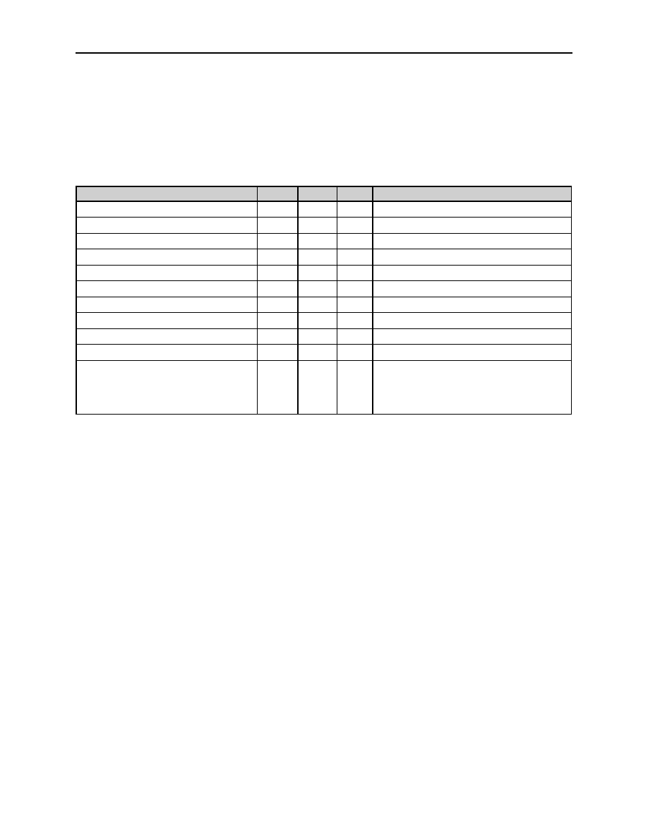
5 Electrical Characteristics
V
DD
= +3.0V ±10% or +5.0V ±10%, V
REFH
= V
DD
, V
REFL
= 0V, -40∫C
T
AMB
+85∫C (unless otherwise specified).
Table 3. Electrical Characteristics
Symbol
Parameter
Conditions
Min
Typ
1
Max
Unit
Static Accuracy (specifications apply to all DACs)
N
Resolution
8
Bit
INL
Integral Non-Linearity Error
-0.75
±0.15 +0.75
LSB
DNL
Differential Non-Linerarity
Guaranteed Monotonic
-0.5
±0.1
+0.5
LSB
G
FSE
Full-Scale Error
-1
±0.2
+1
LSB
V
ZSE
Zero-Code Error
-0.5
±0.1
+0.5
LSB
R
OUT
DAC Output Resistance
3
5
8
k
R/R
OUT
Output Resistance Match
1
%
Reference Input
V
REFH
High Voltage
Input Range
2
0
V
DD
V
V
REFL
Low Voltage Input Range
(AS1505 Only)
3
0
V
DD
V
R
IN
Input Resistance
4
Digital Inputs = 55h, V
REFH
V
DD
625
C
REFH
High Reference Input
Capacitance
5
Digital Inputs = All 0s
60
pF
C
REFL
Low Reference Input
Capacitance
5
Digital Inputs = All 1s
60
pF
Digital Inputs
V
IH
Logic High
V
DD
= +5V
2.4
V
V
DD
= +3V
2.1
V
IL
Logic Low
V
DD
= +5V
0.8
V
V
DD
= +3V
0.6
I
IL
Input Current
V
IN
= 0 or +5V
±1
µA
C
IL
Input Capacitance
5
5
pF
Power Supplies
6
V
DDRANGE
Power Supply Range
2.7
5.5
V
I
DD
Supply Current
(CMOS)
V
IH
= V
DD
or V
IL
= 0V
0.01
5
µA
Supply Current
(TTL)
V
IH
= 2.4V or V
IL
= 0.8V, V
DD
= +5.5V
1
4
mA
I
REFH
Shutdown Current
SHDNN = 0V
0.01
5
µA
P
DISS
Power Dissipation
V
IH
= V
DD
or V
IL
= 0V, V
DD
= +5.5V
27.5
µW
PSRR
Power Supply Rejection
Ratio
V
DD
= +5V ±10%, V
REFH
= +4.5V
0.001 0.002
%/%
V
DD
= +3V ±10%, V
REFH
= +2.7V
0.01
Dynamic Performance
5
t
S
Positive or Negative V
OUT
Settling Time
±0.5 LSB Error Band
0.5
µs
CT
Crosstalk
7
90
dB
www.austriamicrosystems.com
Revision 1.0
4 - 17
AS1504, AS1505
austria
micro
systems
Data Sheet
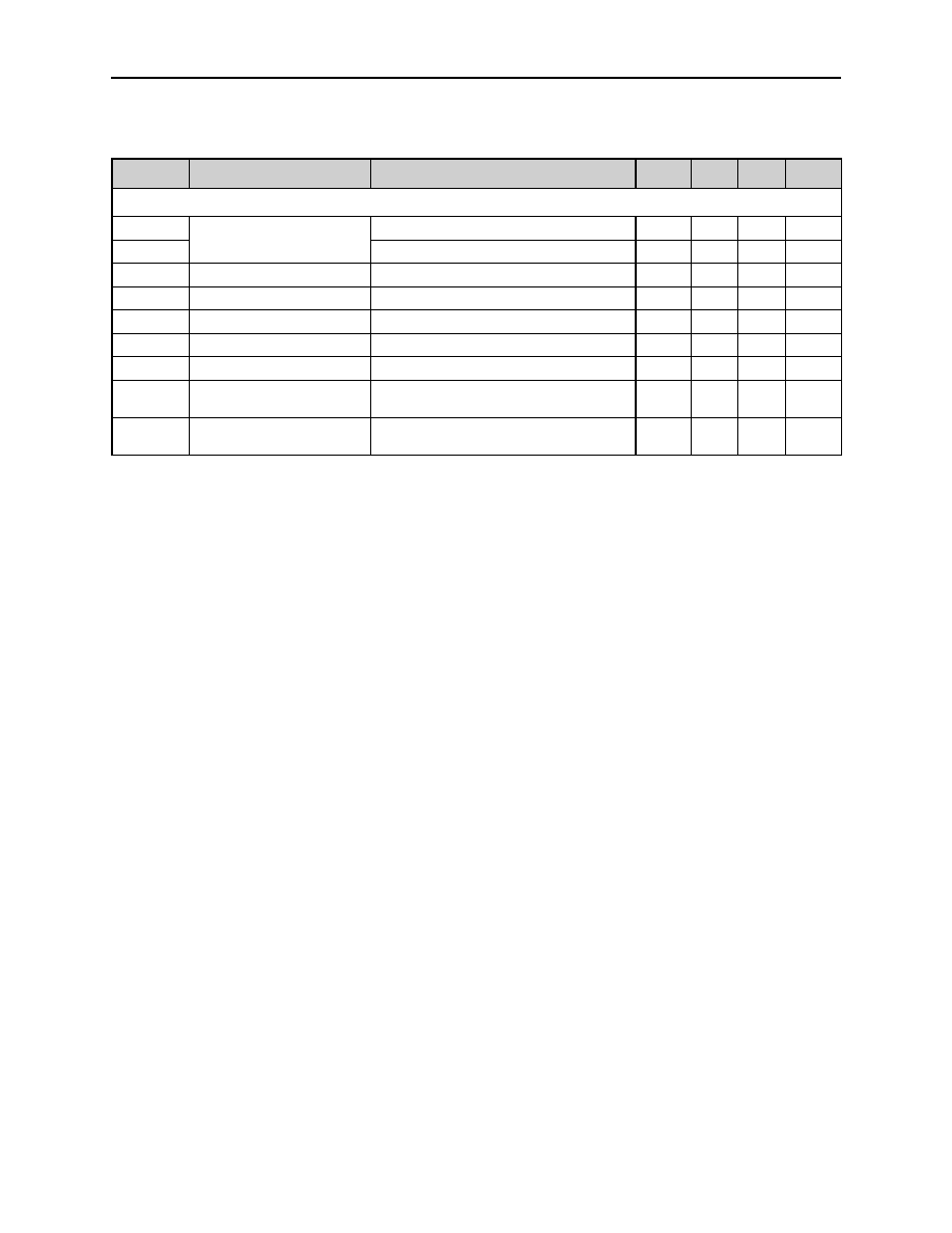
Switching Characteristics
5,
8
t
CH
Input Clock Pulse Width
High Clock Level
15
ns
t
CL
Low Clock Level
15
ns
t
DS
Data Setup Time
5
ns
t
DH
Data Hold Time
5
ns
t
CSS
CSN Setup Time
10
ns
t
CSW
CSN High Pulse Width
10
ns
t
RS
Reset Pulse Width
60
ns
t
CSH
CLK-Rise to CSN-Rise
Hold Time
15
ns
t
CS1
CSN-Rise to Next Rising
Clock Time
10
ns
1. Typ values are average readings at +25∫C.
2. V
REFH
can be any value between V
DD
and GND.
3. V
REFL
can be any value between V
DD
and GND.
4. With all DACs set to code 0x55h. Typical input resistance per DAC is 5kOhm with code 0x55h.
5. Guaranteed by design; not subject to production test.
6. V
IN
= 0V or V
DD
(CMOS); DAC outputs unloaded. P
DISS
is calculated as I
DD
x V
DD
.
7. Measured at an OUTx pin where an adjacent OUTx pin is making a full-scale voltage change.
8. See
Figure 13 on page 9
for location of measured values. All input control voltages are specified with t
R
= t
F
=
2ns.
Table 3. Electrical Characteristics (Continued)
Symbol
Parameter
Conditions
Min
Typ
1
Max
Unit

www.austriamicrosystems.com
Revision 1.0
5 - 17
AS1504, AS1505
austria
micro
systems
Data Sheet
6 Typical Operating Characteristics
Figure 2. Differential Non-Linearity; V
DD
= 2.7V,
Figure 3. Integral Non-Linearity; V
DD
= 2.7V,
V
REFH
= 2.7V, V
REFL
= 0V, T
AMB
= -40, +25, and +85∫C
V
REFH
= 2.7V, V
REFL
= 0V, T
AMB
= -40, +25, and +85∫C
Figure 4. Reference Current vs. Code;
Figure 5. Reference Current vs. Code;
V
DD
= 2.7V, V
REFH
= 2.7V, V
REFL
= 0V
V
DD
= 5.5V, V
REFH
= 5.5V, V
REFL
= 0VReference C.
Figure 6. DNL vs. Channel;
Figure 7. Offset Error vs. Channel;
V
DD
= 2.7V, T = 25∫C
V
DD
= 2.7V, T = 25∫C, all DACs (except selected) = 0x00h
-0.6
-0.4
-0.2
0
0.2
0.4
0.6
0
32
64
96 128 160 192 224 256
Code
INL (LSB)
.
-0.6
-0.4
-0.2
0
0.2
0.4
0.6
0
32
64
96 128 160 192 224 256
Code
DNL (LSB)
.
0
250
500
750
1000
1250
0
32 64
96 128 160 192 224 256
Code
I
RE
F
per DAC (µA)
.
0
100
200
300
400
500
0
32
64
96 128 160 192 224 256
Code
I
RE
F
per DAC (µA)
.
-0.1
0
0.1
0.2
0
1
2
3
4
5
6
7
8
Channel
Offset Error (LSB)
)
0
0
.00005
0.0001
0.00015
0.0002
0
1
2
3
4
5
6
7
8
Channel
Offset Error (LSB)
)
MAX
MIN

www.austriamicrosystems.com
Revision 1.0
6 - 17
AS1504, AS1505
austria
micro
systems
Data Sheet
Figure 8. Gain Error vs. Channel;
Figure 9. Output Resistance vs. Channel;
V
DD
= 2.7V, T = 25∫C, all DACs (except selected) = 0x00h V
DD
= 2.7V, T = 25∫C, all DACs (except selected) = 0x00h
0
0.1
0.2
0.3
0
1
2
3
4
5
6
7
8
Channel
Gain Error (LSB)
.
5500
5520
5540
5560
5580
5600
0
1
2
3
4
5
6
7
8
Channel
Out
put
Resist
ance (Ohm)
.

www.austriamicrosystems.com
Revision 1.0
7 - 17
AS1504, AS1505
austria
micro
systems
Data Sheet
Pin Assignments
7 Pinout
Pin Assignments
Figure 10. Pin Assignments (Top View)
Pin Descriptions
Table 4. Pin Descriptions
Pin Number
Pin Name
Description
(see Figure 10)
CLK
Serial Clock Input
. Positive-edge triggered.
CSN
Chip Select
. When this active-low pin goes high, the serial input register data is
decoded based on the address bits and loaded into the target DAC register.
GND
Ground
OUT1
DAC 1 Output
. DAC 1 address = 000
2
.
OUT2
DAC 2 Output
. DAC 1 address = 001
2
.
OUT3
DAC 3 Output
. DAC 1 address = 010
2
.
OUT4
DAC 4 Output
. DAC 1 address = 011
2
.
OUT5
DAC 5 Output
. DAC 1 address = 100
2
.
OUT6
DAC 6 Output
. DAC 1 address = 101
2
.
OUT7
DAC 7 Output
. DAC 1 address = 110
2
.
OUT8
DAC 8 Output
. DAC 1 address = 111
2
.
RSN
Reset
(AS1504 Only). Active-low asynchronous reset to mid-scale output setting.
Loads all DAC latches with 80
h
.
SDI
Serial Data Input
SHDNN
Shutdown
. Active-low reference input open-circuit. All DAC outputs open-circuit.
Note:
DAC latch settings are maintained during shutdown.
V
DD
Positive Supply Voltage
. +3 to +5V.
V
REFH
Common High-Side DAC Reference Input
V
REFL
Common Low-Side DAC Reference Input
(AS1505 Only).
1
V
REFH
AS1504
2
OUT1
3
OUT2
4
OUT3
5
OUT4
6
SHDNN
7
CSN
16
V
DD
15
RSN
14
OUT8
13
OUT7
12
OUT6
11
OUT5
10
SDI
9
CLK
8
GND
1
V
REFH
AS1505
2
OUT1
3
OUT2
4
OUT3
5
OUT4
6
SHDNN
7
CSN
16
V
DD
15
OUT8
14
OUT7
13
OUT6
12
OUT5
11
SDI
10
CLK
9
V
REFL
8
GND

www.austriamicrosystems.com
Revision 1.0
8 - 17
AS1504, AS1505
austria
micro
systems
Data Sheet
8 Detailed Description
The AS1504/AS1505 contain eight DAC channels of programmable voltage output adjustment capability. OUTx can be
individually changed in random sequence. The fast serial-data loading (33MHz) allows all eight DACs to be quickly
loaded (3ms typ; 12 x 8 x 30ns).
Figure 11. Detailed Block Diagram
Each output voltage can be programmed by clocking an 11-bit serial data word into pin SDI
(see Figure 12)
. The format
of this data word is three address bits (MSB first, followed by eight data bits
(see Table 5)
).
To determine which of the DAC registers is to receive the serial register data (bits B7:B0) the DACx address is
decoded as:
DACx = A2 x 4 + A1 x 2 + A0 + 1
(EQ 1)
Figure 12. Timing Diagram
OUT1
OUT8
AS1504 Only
RSN
AS1505 Only
V
REFL
SDI
CLK
CSN
AS1504/
AS1505
SHDNN
V
REFH
Address
Decode
EN
Serial
Register
D10
D9
D8
D
8
GND
DAC1
Register
D7
D6
D5
D4
D3
D2
D0
D1
D7
D6
D5
D4
D3
D2
D1
D0
DAC8
Register
D7
D6
D5
D4
D3
D2
D1
D0
R
R
DAC1
DAC1
8
8
SDI
CLK
CSN
1
0
1
0
1
0
+5V
0V
DAC Register Load
A2
A0
D7
D6
D5
D4
D3
D2
D1
DO
A1
V
OUT

www.austriamicrosystems.com
Revision 1.0
9 - 17
AS1504, AS1505
austria
micro
systems
Data Sheet
The AS1504 provides a mid-scale reset activated by pin RSN which simplifies settings on initial power up. The AS1505
has a high- and low-side reference (pins V
REFH
and V
REFL
) to determine independent positive full-scale and zero-scale
settings to optimize resolution. -
Both devices feature a power-on reset which resets them to mid-scale.
Both models feature a low-power shutdown mode which places the device into low power-consumption mode resulting
in only leakage currents being consumed from the power supply, V
REFx
inputs, and all 8 outputs. In shutdown mode the
DACx latch settings are maintained. When returning to normal operation from shutdown mode, the DACx outputs
return to their previous voltage settings.
Figure 13. Serial Data Input Timing Diagram; RSN = 1
Figure 14. Reset Timing Diagram
Table 5. AS1504/AS1505
Serial Data Word Format
Address Bits
Data Bits
B10
B9
B8
B7
B6
B5
B4
B3
B2
B1
B0
A2
A1
A0
D7
D6
D5
D4
D3
D2
D1
D0
MSB LSB
MSB
LSB
2
10
2
9
2
8
2
7
2
6
2
5
2
4
2
3
2
2
2
1
2
0
t
CL
t
CSH
t
CH
t
DS
t
CS1
t
CSW
t
S
± 1 LSB Error Band
SDI
CLK
CSN
Ax or Dx
Ax or Dx
1
0
1
0
1
0
+5V
0V
± 1 LSB
t
DH
t
CSS
V
OUT
V
OUT
+5V
+2.5V
± 1 LSB Error Band
± 1 LSB
RSN
1
0
t
RS
t
S

www.austriamicrosystems.com
Revision 1.0
10 - 17
AS1504, AS1505
austria
micro
systems
Data Sheet
Programming The Output Voltage
Figure 15. Equivalent DAC Circuit
Programming The Output Voltage
The output voltage range is determined by the external reference connected to pins V
REFH
and V
REFL
(see
Figure 15
on page 10
for a simplified diagram of the equivalent DAC circuit).
V
REFL
for the AS1504 is internally connected to GND and therefore cannot be offset. Pin V
REFH
can be tied to V
DD
and
pin V
REFL
can be tied to GND establishing a basic rail-to-rail output voltage programming range. Other output ranges
are established by the use of different external voltage references.
The programmed output voltage is determined as:
V
OUT
(Dx) = (Dx)/256 x (V
REFH
≠ V
REFL
) + V
REFL
(EQ 2)
Where:
Dx is the data contained in the 8-bit DACx latch.
For example, when V
REFH
= +5V and V
REFL
= 0V the output voltages will be generated per the codes listed in
Table 6
.
Reference Inputs
The reference input pins (V
REFH
and V
REFL
) set the output voltage range of all eight DACs. For the AS1504, only pin
V
REFH
is available to establish a programmable full-scale output voltage.
Note:
The external reference voltage can be any value between 0 and V
DD
but must not exceed V
DD
.
The AS1505 uses pin V
REFL
to establish the zero-scale output voltage. Any voltage can be applied between 0 and
V
DD
. V
REFL
can be smaller or larger than V
REFH
since the DAC design uses fully bi-directional switches as shown in
Figure 15
. The input resistance to the DAC has a code dependent variation that has a nominal worst case measured at
55
h
, which is approximately 2k
. When V
REFH
is greater than V
REFL
, the REFL reference must be able to sink current
out of the DAC ladder, while the REFH reference is sourcing current into the DAC ladder. The DAC design minimizes
reference glitch current, thus maintaining minimum interference between DAC channels during code changes.
Table 6. Output Voltages
Data Bits
V
OUTx
Output State (V
REFH
= +5V, V
REFL
= 0V)
255 4.98V
Full-Scale
128
2.50V
Half-Scale (Mid-Scale Reset Value)
1 0.02V
1
LSB
0 0.00V
Zero-Scale
GND
DAC
Register
D7
D6
D0
V
REFL
V
REFH
LSB
MSB
P CH
N CH
2R
2R
2R
2R
R
R
To other DACs
Ox

www.austriamicrosystems.com
Revision 1.0
11 - 17
AS1504, AS1505
austria
micro
systems
Data Sheet
DAC Outputs
DAC Outputs
The 8 DAC outputs (OUT1:OUT8) present a constant output resistance of approximately 5k
independent of code set-
tings. The distribution of R
OUT
from DAC to DAC typically matches within ±1%. Device-to-device matching is process-
lot dependent with a ±20% variation. The change in R
OUT
with temperature has a 500 ppm/∞C temperature coefficient.
Note:
During shutdown the OUTx outputs are open-circuited.
Serial Interface
The AS1504/AS1505 are controlled via a standard three-wire serial input. The three input pins are CLK, CSN and SDI.
The positive-edge sensitive CLK input requires a clean transition to avoid clocking spurious data into the serial input
register (standard logic families are perfectly adequate). If mechanical switches are used for device evaluation, they
should be de-bounced by a flip-flop or other suitable means.
Figure 11 on page 8
shows details of the internal digital circuitry. When CSN is pulled low, the clock can load data into
the serial register on each positive clock edge
(see Table 7)
.
The data setup and data hold times in
Table 3 on page 3
determine the valid data time requirements. The last 11 bits of
the data word entered into the serial register are held when CSN goes high. When CSN goes high it gates the address
decoder which enables one of the eight positive-edge triggered DAC registers
(see Figure 16)
.
Figure 16. Equivalent Control Logic
The target DAC register is loaded with the last eight bits of the serial data word completing one DAC update. To
change all eight output settings, eight separate 11-bit data words must be clocked in to the device.
Note:
All digital inputs (CSN, SDI, RSN, SHDNN, and CLK) are protected with the series input resistor and parallel
zener diode ESD circuit illustrated in
Figure 17
.
Figure 17. Equivalent ESD Protection Circuit
Note:
Digital inputs can be driven by voltages exceeding V
DD
thus providing logic level translation from 5V logic when
the device is operated from a 3V supply.
Table 7. Function of Pins CSN and CLK
CSN
CLK
Register Activity
1 X
No effect.
0 Positive
Edge
Shifts serial register one bit loading the next bit in from the SDI pin.
Positive Edge
X
Data is transferred from the serial register to the decoded DAC register
(see Figure
16)
.
Address
Decode
DAC1
Serial
Register
DAC2
DAC8
SDI
CLK
CSN
AS1504/
AS1505
Logic
50

www.austriamicrosystems.com
Revision 1.0
12 - 17
AS1504, AS1505
austria
micro
systems
Data Sheet
Supply Bypassing
9 Application Information
Supply Bypassing
The AS1504/AS1505 require a well-filtered power source. In most applications, the AS1504/AS1505 should be pow-
ered directly from the system power supply (+3 to +5V). However, if the logic supply is a switch-mode design, it will
probably generate noise in the 20kHz to 1MHz range. Additionally, fast logic gates can generate transients hundred of
millivolts in amplitude from wiring resistance and inductance.
The circuit shown in
Figure 18
isolates the analog section from any logic switching transients. Even if a separate power
supply trace is not available, adequate supply bypassing will reduce supply-line induced errors. Local supply bypass-
ing consisting of a 10µF tantalum electrolytic capacitor in parallel with a 0.1µF ceramic capacitor is recommended
(see
Figure 19)
.
Figure 18. Power Supply Traces
Figure 19. Recommended Supply Bypassing
Output Buffering
For most designs, the nominal 5k
output impedance of the AS1504/AS1505 is sufficient to drive succeeding circuitry.
If a lower output impedance is required, an external amplifier can be added
(see Figure 20 on page 13)
.
A single amplifier should be used as a simple buffer to reduce the output resistance of DAC1. An amplifier with low off-
set voltage, low supply current, and operation at less than 3V is recommended due to its rail-to-rail input and output
operation. DAC2 and DAC3 are configured in a summing arrangement where DAC3 provides the coarse output volt-
age setting and DAC2 is used for fine adjustments.
The use of R
1
in series with DAC2
(see Figure 20 on page 13)
attenuates its contribution to the voltage sum node at the
output of DAC3.
0.1µF
CMOS/TTL
Logic Circuits
+5V Power
Supply
10µF
Tantalum
AS1504/
AS1505
+
0.1µF
10µF
Tantalum
AS1504/
AS1505
+
+5V
16 V
DD
8 GND

www.austriamicrosystems.com
Revision 1.0
13 - 17
AS1504, AS1505
austria
micro
systems
Data Sheet
Increasing Output Voltage Swing
Figure 20. Output Buffering
Increasing Output Voltage Swing
An external amplifier can be used to extend the output voltage swing beyond the power supply rails of the AS1504/
AS1505. This design allows for a simple digital interface to the DAC, while expanding the output swing to take advan-
tage of higher voltage external power supplies (e.g., DAC 1 of
Figure 21
is configured to swing from -5 to +5V). The
actual output voltage is given by:
V
OUT
= (1+ (R
F
/R
S
))((D/256)5V) - 5V
(EQ 3)
Where:
D is the DAC input value (i.e., 0 to 255).
This design can be combined with the circuit in
Figure 20
if very accurate adjustments around 0V are required.
Figure 21. Increasing Output Voltage Swing
DAC 2 (non-inverting A
V
= 2 configuration) of
Figure 21
increases the available output swing to +10V. The feedback
resistors can be adjusted to provide scaling of the output voltage, within the limits of the external operational amplifier
power supplies.
≠
+
V
H
AS1504/
AS1505
GND
V
REFL
V
DD
V
L
V
H
V
L
V
H
V
L
V
REFH
Amplifier
≠
+
100k
R
1
Simple Buffer
0 to 5V
Summer Circuit with
Fine Trim Adjustment
+5V
DAC1
DAC2
DAC3
DAC1
OUT1
DAC2
AS1504/
AS1505
GND
V
REFL
AS1505
Only
OUT2
≠
+
100k
100k
0 to +10V
≠
+
100k
-5 to +4.98V
100k
V
DD
V
REFH
+5V
-5V
+12V
R
F
R
S
+5V

www.austriamicrosystems.com
Revision 1.0
14 - 17
AS1504, AS1505
austria
micro
systems
Data Sheet
Microprocessor Interfaces
Microprocessor Interfaces
The AS1504/AS1505 serial interface provides a simple connection to a wide range of microprocessors, most of which
have built-in serial data capability that can be used for communicating with the device.
Note:
In cases where a serial port is not available on the microprocessor, the AS1504/AS1505 can be addressed via
software.
Eleven data bits are required to load data into the AS1504/AS1505 (3 bits for the DAC address and 8 bits for the DAC
value). If more than eleven bits are transmitted before the microprocessor chip select input goes high, the most-signifi-
cant bits are ignored. Because most microprocessors transmit data in 8-bit words, it will need to send 16 bits to the
AS1504/AS1505; however, the AS1504/AS1505 only responds to the last 11 bits clocked into the SDI input, so the
serial data interface is not affected.
8051 Microprocessor Interface
Figure 22
shows the AS1504/AS1505 interface to an 8051 microprocessor. This interface uses the 8051 internal serial
port as a simple 8-bit shift register (Mode 0 operation). 8051 Port3.0 serves as the serial data output port and Port3.1
serves as the serial clock.
Figure 22. AS1504-to-8051 Microprocessor Interface
As data is written to the serial buffer register (SBUF, at Special Function Register location 99
h
), the data is automati-
cally converted to serial format and clocked out via Port3.0 and Port3.1. Once 8 bits have been transmitted, the trans-
mit interrupt flag (SCON.1) is set and the next 8 bits can be transmitted.
The AS1504/AS1505 requires that CSN goes low at the start of the serial data transfer. Additionally, pin CLK must be
high when CSN goes high at the end of each data transfer. The 8051 serial clock meets these requirements, since
Port3.1 begins and ends the serial data transfer in a high state.
AS1504
OUT8
OUT1
SDI
CLK
RSN
SHDNN
CSN
8051
Port3.0
Port3.1
Port1.3
Port1.2
Port1.1
RX
TX
Serial Data
Shift Register
Shift Clock
1.1
1.2
1.3
Port 1
V
DD
V
REFH
0.1µF
10µF
Tantalum
+
+5V

www.austriamicrosystems.com
Revision 1.0
15 - 17
AS1504, AS1505
austria
micro
systems
Data Sheet
10 Package Drawings and Markings
The AS1504/AS1505 is available in a 16-pin SOIC-150 package.
Figure 23. 16-pin SOIC-150 Package
Symbol
Min
Max
A
1.52
1.72
A1
0.10
0.25
A2
1.37
1.57
B
0.36
0.46
C
0.19
0.25
D
9.80
9.98
E
3.81
3.99
e
1.27BSC
H
5.80
6.20
h
0.25
0.50
L
0.41
1.27
0∫
8∫
ZD
0.51 REF
Notes:
1. Lead coplanarity should be 0 to 0.10mm (.004") max.
2. Package surface finishing:
- Top, matte (charmilles #18-30)
- All sides, matte (charmilles +18-30)
- Bottom, smooth or matte (charmilles +18-30)
3. All dimensions excluding mold flashes and end flash from the pack-
age body shall not exceed 0.25mm (.010") per side.
4. Details of pin #1 mark are optional but must be located within the
area indicated.
www.austriamicrosystems.com
Revision 1.0
16 - 17
AS1504, AS1505
austria
micro
systems
Data Sheet
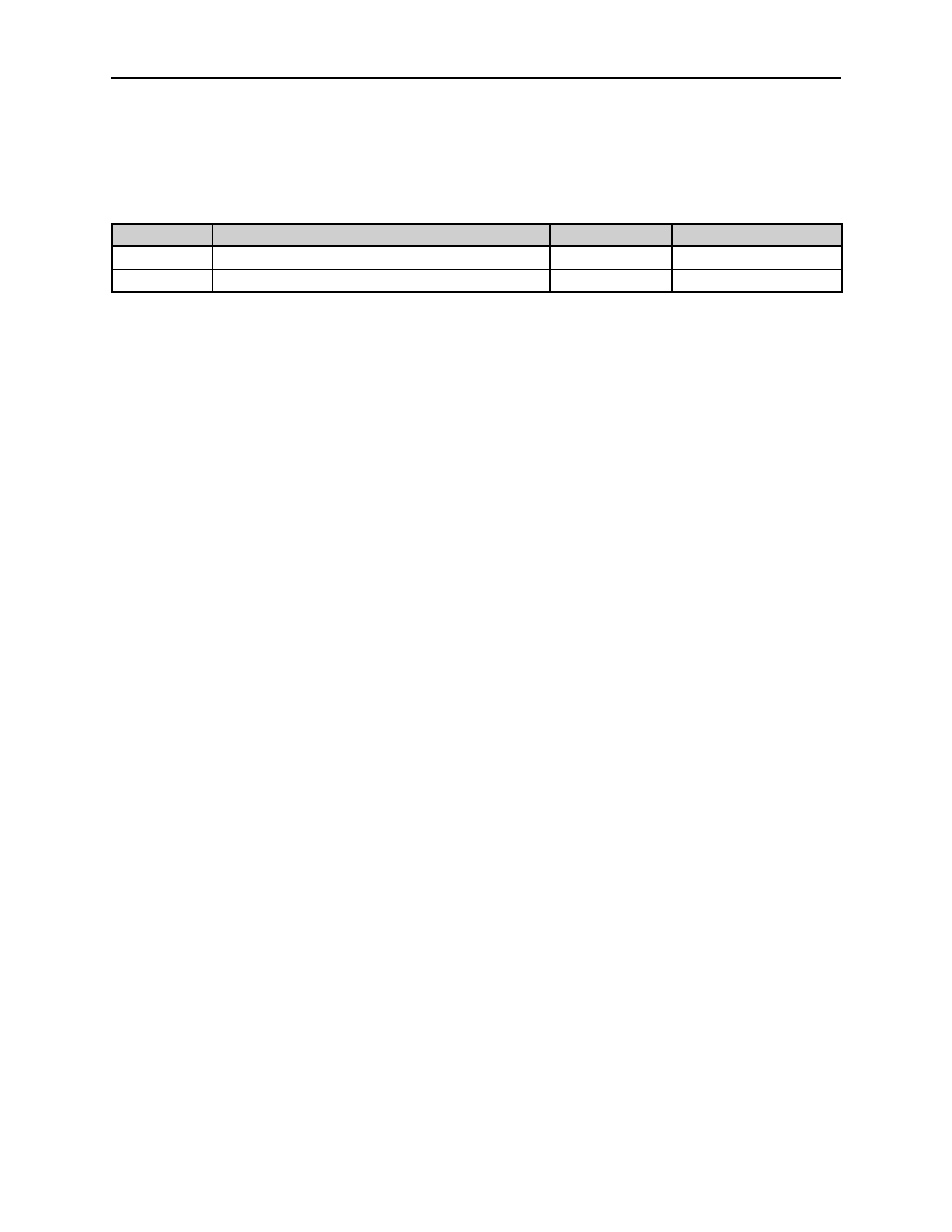
11 Ordering Information
The devices are available as the standard products shown in
Table 8
.
Table 8. Ordering Information
Model
Description
Delivery Form
Package
AS1504-T
Octal 8-Bit DAC, Mid-Scale Reset
Tape and Reel
16-pin SOIC-150 Narrow
AS1505-T
Octal 8-Bit DAC, Separate V
REFL
Range Settings
Tape and Reel
16-pin SOIC-150 Narrow

www.austriamicrosystems.com
Revision 1.0
17 - 17
AS1504, AS1505
austria
micro
systems
Data Sheet
Copyrights
Copyright © 1997-2006, austriamicrosystems AG, Schloss Premstaetten, 8141 Unterpremstaetten, Austria-Europe.
Trademarks Registered Æ. All rights reserved. The material herein may not be reproduced, adapted, merged, trans-
lated, stored, or used without the prior written consent of the copyright owner.
All products and companies mentioned are trademarks or registered trademarks of their respective companies.
Disclaimer
Devices sold by austriamicrosystems AG are covered by the warranty and patent indemnification provisions appearing
in its Term of Sale. austriamicrosystems AG makes no warranty, express, statutory, implied, or by description regarding
the information set forth herein or regarding the freedom of the described devices from patent infringement. austriami-
crosystems AG reserves the right to change specifications and prices at any time and without notice. Therefore, prior
to designing this product into a system, it is necessary to check with austriamicrosystems AG for current information.
This product is intended for use in normal commercial applications. Applications requiring extended temperature
range, unusual environmental requirements, or high reliability applications, such as military, medical life-support or life-
sustaining equipment are specifically not recommended without additional processing by austriamicrosystems AG for
each application. For shipments of less than 100 parts the manufacturing flow might show deviations from the standard
production flow, such as test flow or test location.
The information furnished here by austriamicrosystems AG is believed to be correct and accurate. However,
austriamicrosystems AG shall not be liable to recipient or any third party for any damages, including but not limited to
personal injury, property damage, loss of profits, loss of use, interruption of business or indirect, special, incidental or
consequential damages, of any kind, in connection with or arising out of the furnishing, performance or use of the tech-
nical data herein. No obligation or liability to recipient or any third party shall arise or flow out of
austriamicrosystems AG rendering of technical or other services.
Contact Information
Headquarters
austriamicrosystems AG
A-8141 Schloss Premstaetten, Austria
Tel: +43 (0) 3136 500 0
Fax: +43 (0) 3136 525 01
e-mail:
info@austriamicrosystems.com
For Sales Offices, Distributors and Representatives, please visit:
http://www.austriamicrosystems.com
austria
micro
systems
≠ a leap ahead