 | –≠–ª–µ–∫—Ç—Ä–æ–Ω–Ω—ã–π –∫–æ–º–ø–æ–Ω–µ–Ω—Ç: AS1752 | –°–∫–∞—á–∞—Ç—å:  PDF PDF  ZIP ZIP |

AS1751 , AS1752, AS1753
High-Speed, Low-Voltage, Single-Supply,
0.9
, Quad SPST Analog Switches
www.austriamicrosystems.com
Revision 1.4
1 - 16
austria
micro
systems
D a ta S h e e t
1 General Description
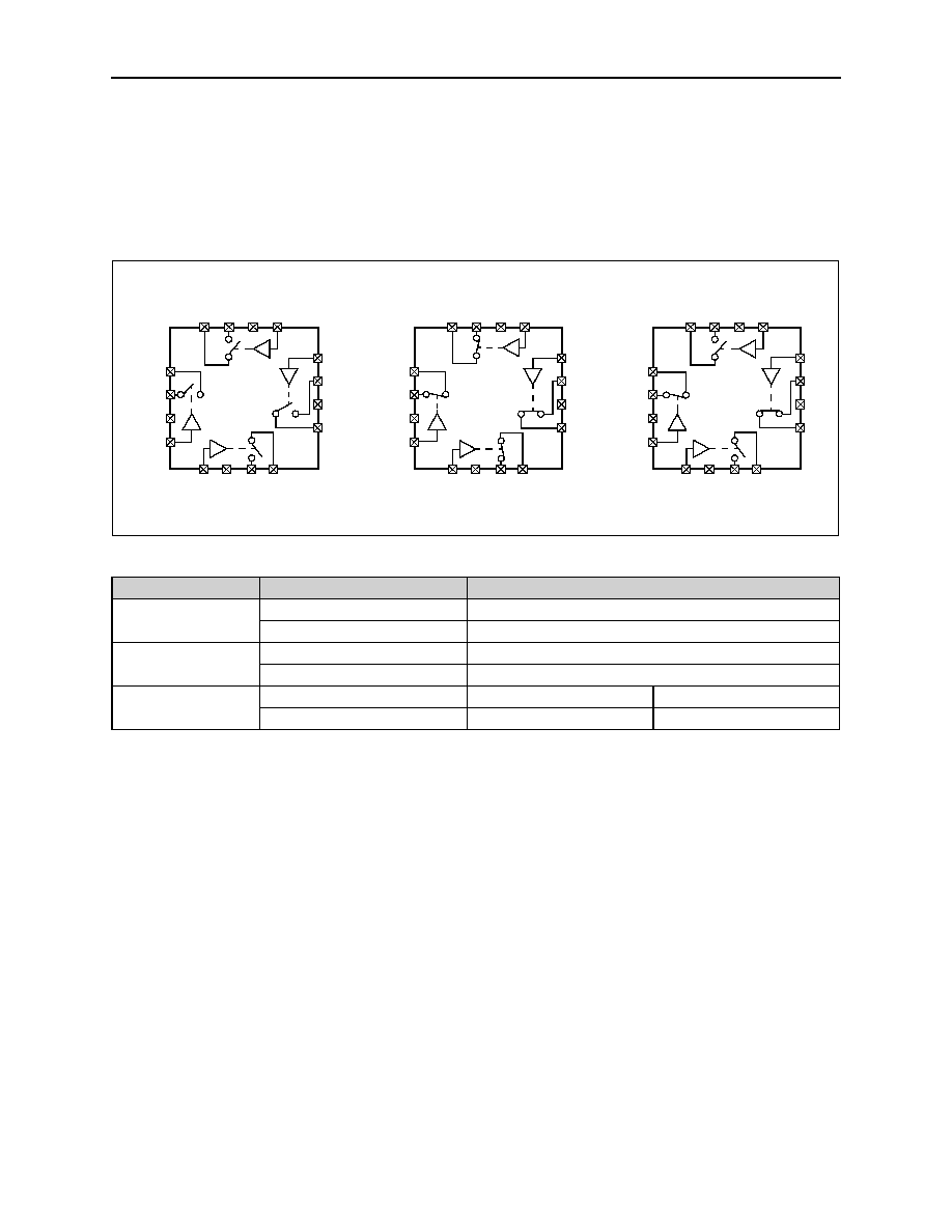
The AS1751/AS1752/AS1753 are high-speed, low-volt-
age, quad single-pole/single-throw (SPST) analog
switches.
Fast switching speeds, low ON-resistance, and low
power consumption make these devices ideal for single-
cell battery powered applications.
These highly-reliable devices operate from a single +1.6
to +3.6V supply, and are differentiated by the type and
number of switches:
!
AS1751 ≠ Four normally open (NO) switches
!
AS1752 ≠ Four normally closed (NC) switches
!
AS1753 ≠ Two NO switches and Two NC switches
The AS1753 supports break-before-make switching.
With very low ON-resistance (R
ON
), R
ON
matching and
R
ON
flatness, the devices can accurately switch signals
for sample and hold circuits, digital filters, and op-amp
gain switching networks.
The AS1751/AS1752/AS1753 digital logic input is 1.8V
CMOS-compatible when using a +3V supply, and all
devices can handle Rail-to-Rail signals.
The devices are available in a 3mm x 3mm 16-pin QFN
package and a 14-pin TSSOP package.
Figure 1. 14-pin TSSOP Block Diagrams
2 Key Features
!
ON-Resistance:
- 0.9
(+3V supply)
- 2.5
(+1.8V supply)
!
R
ON
Matching:
- 0.12
(+3V supply)
- 0.25
(+1.8V supply)
!
R
ON
Flatness: 0.1
(+3V Supply)
!
Supply Voltage Range: +1.6 to +3.6V
!
Switching Speed: t
ON
= 22ns, t
OFF
= 14ns
!
Current-Handling: 250mA Continuous
!
Break-Before-Make Switching (AS1753)
!
Rail-to-Rail Signal Handling
!
1.8V CMOS Logic Compatible (+3V Supply)
!
Operating Temperature Range: -40 to +85∫C
!
Package Types:
- 16-pin QFN (3mm x 3mm)
- 14-pin TSSOP
3 Applications
The devices are ideal for use in power routing systems,
cordless and mobile phones, MP3 players, CD and DVD
players, PDAs, handheld computers, digital cameras,
hard drives, and any other application where high-speed
signal switching is required.
AS1752
1
NC1
2
COM1
3
NC2
4
COM2
5
IN2
6
IN3
7
GND
14
V+
13
IN1
12
IN4
11
NC4
10
COM4
9
COM3
8
NC3
AS1753
1
NO1
2
COM1
3
NC2
4
COM2
5
IN2
6
IN3
7
GND
14
V+
13
IN1
12
IN4
11
NC4
10
COM4
9
COM3
8
NO3
AS1751
1
NO1
2
COM1
3
NO2
4
COM2
5
IN2
6
IN3
7
GND
14
V+
13
IN1
12
IN4
11
NO4
10
COM4
9
COM3
8
NO3
Device
Input
Switch State
AS1751
Low
Off
High
On
AS1752
Low
On
High
Off
AS1753
Low
Switches 1, 3 = Off
Switches 2, 4 = On
High
Switches 1, 3 = On
Switches 2, 4 = Off

AS1751, AS1752, AS1753
austria
micro
systems
Data Sheet
www.austriamicrosystems.com
Revision 1.4
2 - 16
4 Absolute Maximum Ratings
Stresses beyond those listed in Table 1 may cause permanent damage to the device. These are stress ratings only,
and functional operation of the device at these or any other conditions beyond those indicated in Section 5 Electrical
Characteristics on page 3 is not implied. Exposure to absolute maximum rating conditions for extended periods may
affect device reliability.
Signals on pins COM1, COM3, NO1, NO2, NC1, or NC2 that exceed V+ or GND are clamped by internal diodes. For-
ward-diode current should be limited to the maximum current rating.
-
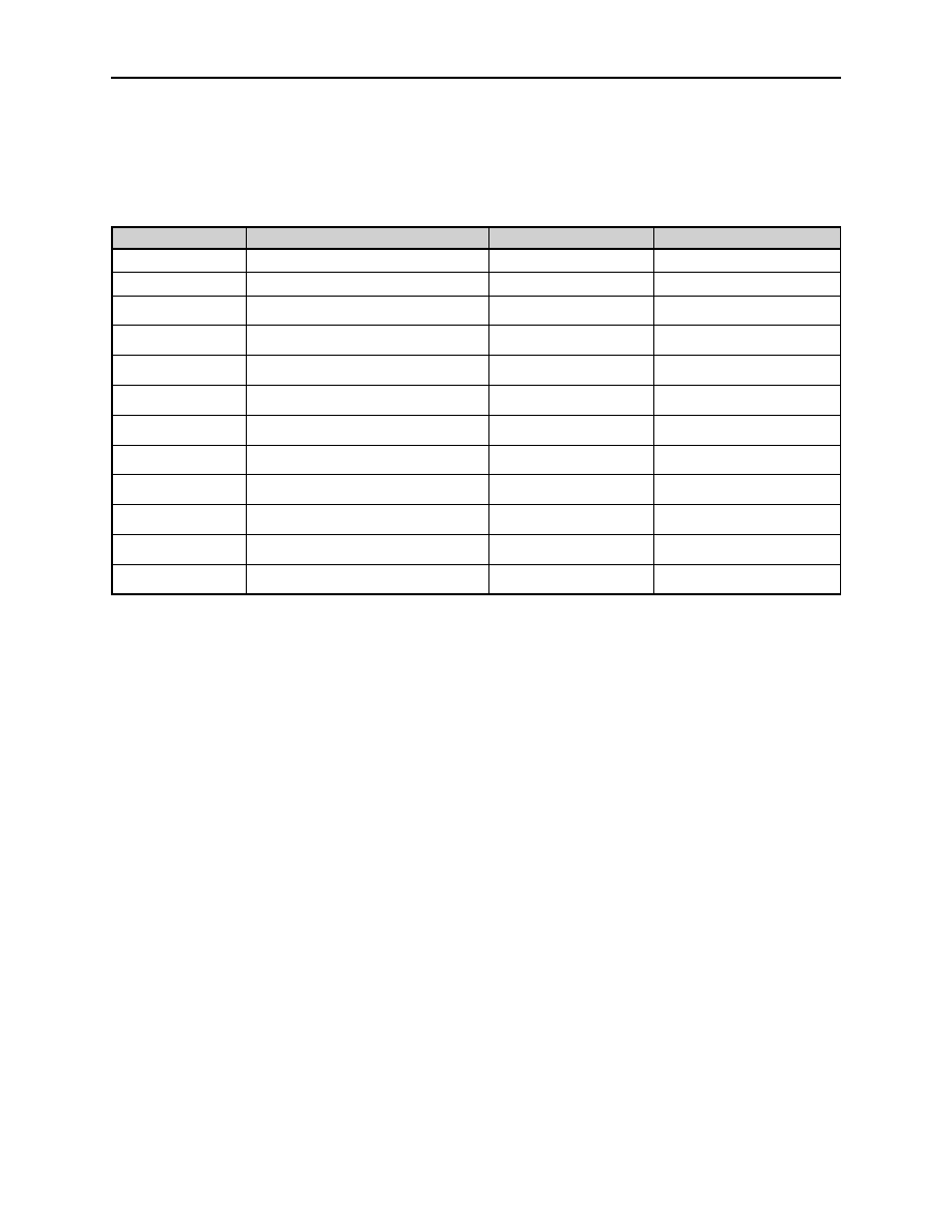
Table 1. Absolute Maximum Ratings
Parameter
Min
Max
Units
Comments
V+, INx to GND
-0.3
+5
V
COMx, NOx, NCx to GND
-0.3
V+
+ 0.3
V
COMx, NOx, NCx Continuous Current
-250
+250
mA
COMx, NOx, NCx Peak Current
-350
+350
mA
Pulsed at 1ms 10% duty cycle
Continuous Power
Dissipation (T
AMB
= +70∫C)
16-pin QFN
727
mW
Derate at 9.1W/∫C above +70∫C
14-pin TSSOP
1349
Derate at 16.9W/∫C above +70∫C
Operating Temperature Range
-40
+85
∫C
Electro-Static Discharge
2500
V
HBM Mil-Std883E 3015.7 methods
Latch Up Immunity
250
mA
Norm: JEDEC 17
Junction Temperature
+150
∫C
Storage Temperature Range
-65
+150
∫C
Package Body Temperature
+260
∫C
The reflow peak soldering temperature (body
temperature) specified is in accordance with
IPC/JEDEC J-STD-020C "Moisture/Reflow
Sensitivity Classification for Non-Hermetic
Solid State Surface Mount Devices"

AS1751, AS1752, AS1753
austria
micro
systems
Data Sheet
www.austriamicrosystems.com
Revision 1.4
3 - 16
5 Electrical Characteristics
V+ = +2.7 to +3.6V, V
IH
= +1.4V, V
IL
= +0.5V, T
AMB
= T
MIN
to T
MAX
(unless otherwise specified). Typ values @ V+ =
+3.0V, T
AMB
= +25∫C.
Table 2. Power Supply Characteristics
Symbol
Parameter
Conditions
Min
Typ
Max Unit
V+
Power Supply Range
T
AMB
= T
MIN
to T
MAX
1.6
3.6
V
I+
Positive Supply
Current
V+ = 3.6V, V
INx
= 0 or V+, T
AMB
= +25∫C
0.1
µA
Table 3. +3V Supply Electrical Characteristics
Symbol
Parameter
Conditions
Min
Typ
Max Unit
Analog Switch
V
COMx
,
V
NOx
, V
NCx
Analog Signal Range
0
V+
V
R
ON
ON-Resistance
V+ = 2.7V, I
COMx
= 100mA,
V
NOx
or V
NCx
= 1.5V
T
AMB
= +25∫C
0.4
0.9
T
AMB
= T
MIN
to T
MAX
1
R
ON
ON-Resistance Match
Between Channels
1
V+ = 2.7V, I
COMx
= 100mA,
V
NOx
or V
NCx
= 1.5V
T
AMB
= +25∫C
0.03
0.12
T
AMB
= T
MIN
to T
MAX
0.15
R
FLAT(ON)
ON-Resistance
Flatness
2
V+ = 2.7V, I
COMx
= 100mA,
V
NOx
or V
NCx
= 1, 1.5, or 2V
T
AMB
= +25∫C
0.02
0.1
T
AMB
= T
MIN
to T
MAX
0.12
I
NOx(OFF)
,
I
NCx(OFF)
NOx or NCx
Off-Leakage Current
V+ = 3.6V,
V
COMx
= 0.3 or 3.6V,
V
NOx
or V
NCx
= 3.6 or 0.3V
T
AMB
= +25∫C
-2.5
+2.5
nA
T
AMB
= T
MIN
to T
MAX
-10
+10
I
COMx(OFF)
COMx Off-Leakage
Current
V+ = 3.6V,
V
COMx
= 0.3 or 3.6V,
V
NOx
or V
NCx
= 3.6 or 0.3V
T
AMB
= +25∫C
-2.5
+2.5
nA
T
AMB
= T
MIN
to T
MAX
-10
+10
I
COMx(ON)
COMx On-Leakage
Current
V+ = 3.6V,
V
COMx
= 0.3 or 3.6V,
V
NOx
or V
NCx
= 0.3 or 3.6V
T
AMB
= +25∫C
-2.5
+2.5
nA
T
AMB
= T
MIN
to T
MAX
-10
+10
Switch Dynamic Characteristics
t
ON
Turn On Time
3
V
NOx
or V
NCx
= 1.5V,
R
LOAD
= 50
, C
LOAD
=
35pF, Figures 11, 12
T
AMB
= +25∫C
16
22
ns
T
AMB
= T
MIN
to T
MAX
24
t
OFF
Turn Off Time
3
V
NOx
or V
NCx
= 1.5V,
R
LOAD
= 50
, C
LOAD
=
35pF, Figures 11, 12
T
AMB
= +25∫C
5
14
ns
T
AMB
= T
MIN
to T
MAX
15
t
BBM
Break-Before-Make
3
V
NOx
or V
NCx
= 1.5V,
R
LOAD
= 50
, C
LOAD
=
35pF, Figure 13 (AS1753)
T
AMB
= +25∫C
11
ns
T
AMB
= T
MIN
to T
MAX
2
Q
Charge Injection
V
GEN
= V+, R
GEN
= 0, C
LOAD
= 1.0nF, Figure 14
2
pC
C
OFF
NOx, NCx
Off-Capacitance
f = 1MHz, Figure 15
45
pF
C
COMx(OFF)
COMx
Off-Capacitance
f = 1MHz, Figure 15
49
pF
C
COMx(ON)
COMx
On-Capacitance
f = 1MHz, Figure 15
85
pF

AS1751, AS1752, AS1753
austria
micro
systems
Data Sheet
www.austriamicrosystems.com
Revision 1.4
4 - 16
V+ = +1.8V, V
IH
= +1.0V, V
IL
= 0.4V, T
AMB
= T
MIN
to T
MAX
(unless otherwise specified). Typ values @ T
AMB
= +25∫C.
1.
R
ON
= R
ON(MAX)
- R
ON(MIN)
.
2. Flatness is defined as the difference between the maximum and the minimum value of ON-resistance as measured
over the specified analog signal ranges.
3. Guaranteed by design.
4. Off-Isolation = 20log10(V
COMx
/V
NOx
), V
COMx
= output, V
NOx
= input to off switch.
5. Between two switches.
V
ISO
Off-Isolation
4
f = 10MHz, R
LOAD
= 50
, C
LOAD
= 5pF, Figure 16
-40
dB
f = 1MHz, R
LOAD
= 50
, C
LOAD
= 5pF, Figure 16
-55
Crosstalk
5
f = 10MHz, R
LOAD
= 50
, C
LOAD
= 5pF, Figure 16
-70
dB
f = 1MHz, R
LOAD
= 50
, C
LOAD
= 5pF, Figure 16
-80
THD
Total Harmonic
Distortion
f = 20Hz to 20kHz, V
COMx
= 2Vp-p, R
LOAD
= 32
0.033
%
Logic Input
V
IH
Input Logic High
1.4
V
V
IL
Input Logic Low
0.5
V
I
IN
Input Leakage Current
V
INx
= 0 or V+
-1
0.0001
+1
µA
Table 4. +1.8V Supply Electrical Characteristics
Symbol
Parameter
Conditions
Min
Typ
Max Unit
Analog Switch
V
COMx
,
V
NOx
, V
NCx
Analog Signal
Range
0
V+
V
R
ON
ON-Resistance
V+ = 1.8V, I
COMx
= 10mA,
V
NOx
or V
NCx
= 0.9V
T
AMB
= +25∫C
0.9
2.5
T
AMB
= T
MIN
to T
MAX
3
R
ON
ON-Resistance
Match Between
Channels
1
V+ = 1.8V, I
COMx
= 10mA,
V
NOx
or V
NCx
= 0.9V
T
AMB
= +25∫C
0.05
0.25
T
AMB
= T
MIN
to T
MAX
0.25
Switch Dynamic Characteristics
t
ON
Turn On Time
3
V
NOx
or V
NCx
= 1.0V,
R
LOAD
= 50
, C
LOAD
= 35pF,
Figures 11, 12
T
AMB
= +25∫C
22
30
ns
T
AMB
= T
MIN
to T
MAX
35
t
OFF
Turn Off Time
3
V
NOx
or V
NCx
= 1.0V,
R
LOAD
= 50
, C
LOAD
= 35pF,
Figures 11, 12
T
AMB
= +25∫C
12
20
ns
T
AMB
= T
MIN
to T
MAX
25
Q
Charge Injection
V
GEN
= V+, R
GEN
= 0, C
LOAD
= 1.0nF, Figure 14
1
pC
Logic Input
V
IH
Input Logic High
1.0
V
V
IL
Input Logic Low
0.4
V
I
IN
Input Leakage
Current
V
INx
= 0 or V+
-1
0.0001
+1
µA
Table 3. +3V Supply Electrical Characteristics (Continued)
Symbol
Parameter
Conditions
Min
Typ
Max Unit

AS1751, AS1752, AS1753
austria
micro
systems
Data Sheet
www.austriamicrosystems.com
Revision 1.4
5 - 16
6 Typical Operating Characteristics
Figure 2. Frequency Response
Figure 3. Total Harmonic Distortion vs. Frequency
Figure 4. Turn On/Turn Off Time vs. Temperature
Figure 5. Turn On/Off Time vs. Supply Voltage
Figure 6. R
ON
vs. V
COM
and Temperature; V
DD
= 2.7V
Figure 7. R
ON
vs. V
COM
-100
-90
-80
-70
-60
-50
-40
-30
-20
-10
0
10
0.01
0.1
1
10
100
1000
Frequency (MHz)
Response (dB)
Bandwidth
0
0.005
0.01
0.015
0.02
0.025
0.03
0.035
0.04
1
10
100
1000
10000 100000
Frequency (Hz)
THD (%)
V
DD
= 3V
0
2
4
6
8
10
12
14
16
18
20
22
24
26
1.6
2
2.4
2.8
3.2
3.6
Supply Voltage (V)
Time
(n
s)
t
ON
t
OFF
0
2
4
6
8
10
12
14
16
18
20
-40
-15
10
35
60
85
Temperature (∞C)
Time (ns)
t
ON
t
OFF
0.20
0.25
0.30
0.35
0.40
0.45
0.50
0
0.5
1
1.5
2
2.5
3
V
COM
(V)
R
ON
(
)
0.3
0.4
0.5
0.6
0.7
0.8
0.9
1.0
0
0.5
1
1.5
2
2.5
3
3.5
V
COM
(V)
R
ON
(
)
Temp = -40∫C
V
DD
= 1.8V
V
DD
= 2.5V
V
DD
= 2.7V
V
DD
= 3V
V
DD
= 3.6V
V
DD
= 2V
V
DD
= 3.3V
Temp = +25∫C
Temp = +85∫C

AS1751, AS1752, AS1753
austria
micro
systems
Data Sheet
www.austriamicrosystems.com
Revision 1.4
6 - 16
Figure 8. Charge Injection vs. V
COM
0
10
20
30
40
50
60
0 0.3 0.6 0.9 1.2 1.5 1.8 2.1 2.4 2.7 3
V
COM
(V)
Q (pC)
V
DD
= 1.8V
V
DD
= 3V
AS1751, AS1752, AS1753
austria
micro
systems
Data Sheet
ON-Resistance
www.austriamicrosystems.com
Revision 1.4
7 - 16
7 Detailed Description
The AS1751/AS1752/AS1753 are low ON-resistance, low-voltage, quad analog SPST switches that operate from a
single +1.6 to +3.6V supply.
CMOS process technology allows switching of analog signals that are within the supply voltage range (GND to V+).
Figure 9. 16-pin QFN Block Diagrams
ON-Resistance
When powered from a +3V supply, the low (0.9
, max) ON-resistance allows high-speed, continuous signals to be
switched in a variety of applications.
Bi-Directional Switching
Pins NOx, NCx, and COMx are bi-directional, thus they can be used as inputs to- or outputs from other components.
Analog Signal Levels
Analog signals ranging over the entire supply voltage range (V+ to GND) can be switched with very little change in ON-
resistance (see Typical Operating Characteristics on page 5).
Logic Inputs
The devices' logic inputs can be driven up to +3.6V regardless of the supply voltage value. For example, with a +1.8V
supply, INx may be driven low to GND and high to +3.6V. This allows the devices to interface with +3V systems using
a supply of less than 3V.
Table 5. Truth Tables
Device
Input
Switch State
AS1751
Low
Off
High
On
AS1752
Low
On
High
Off
AS1753
Low
Switches 1, 3 = Off
Switches 2, 4 = On
High
Switches 1, 3 = On
Switches 2, 4 = Off
AS1751
2
COM2
3
N/C
4
IN2
1
NO2
6
GND
8
COM3
5
IN3
7
NO3
11
NO4
10
N/C
9
COM4
12
IN4
COM1
16
AS1752
2
COM2
3
N/C
4
IN2
1
NC2
6
GND
8
COM3
5
IN3
7
NC3
11
NC4
10
N/C
9
COM4
12
IN4
AS1753
2
COM2
3
N/C
4
IN2
1
NC2
6
GND
8
COM3
5
IN3
7
NO3
11
NC4
10
N/C
9
COM4
12
IN4
NO1
15
V+
14
IN1
13
COM1
16
NC1
15
V+
14
IN1
13
COM1
16
NO1
15
V+
14
IN1
13
AS1751, AS1752, AS1753
austria
micro
systems
Data Sheet
Power Supply Sequencing
www.austriamicrosystems.com
Revision 1.4
8 - 16
8 Application Information
Power Supply Sequencing
Proper power-supply sequencing is critical for proper switch operation. The power supplies should be started up in the
following sequence:
1. V+
2. NOx, NCx, COMx
Note:
Do not exceed the absolute maximum ratings (see page 2).
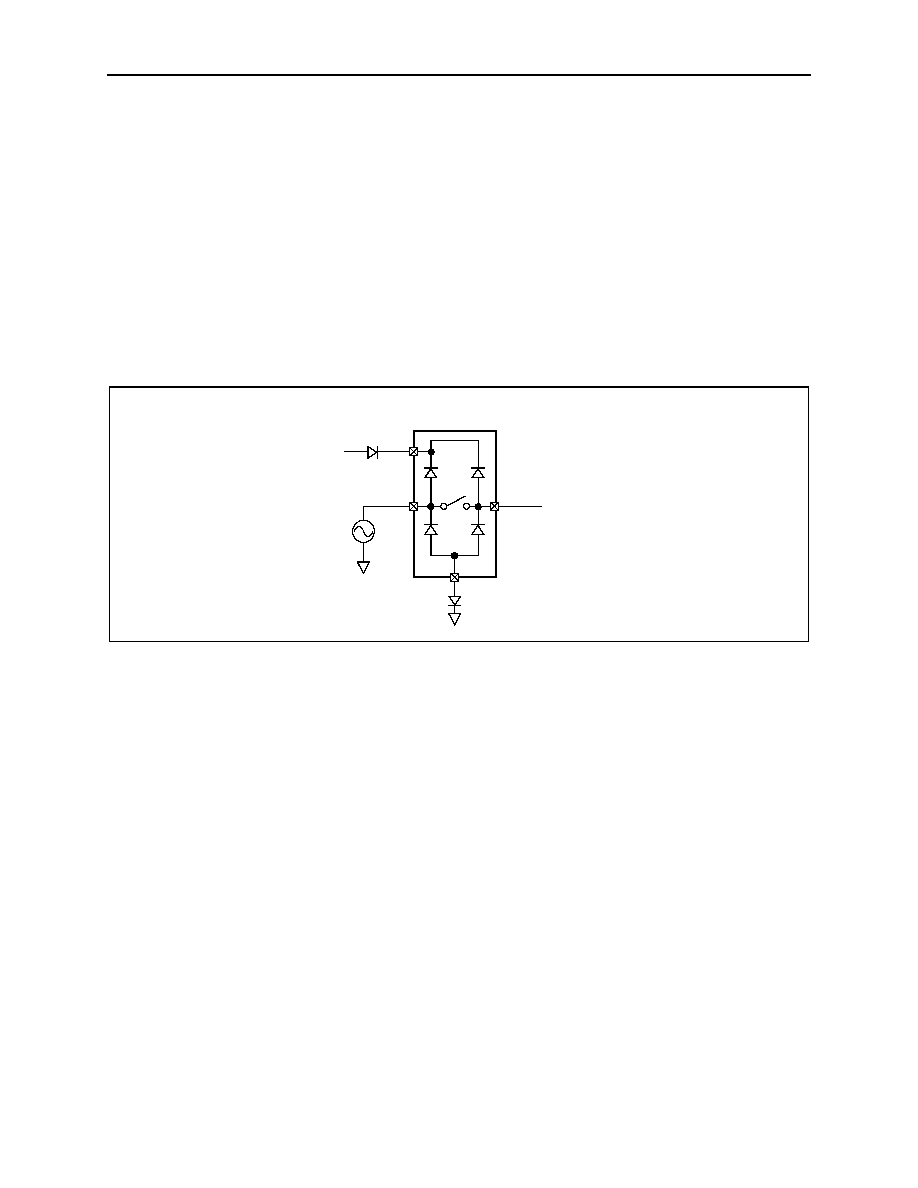
Overvoltage Protection
ON-resistance increases slightly at lower supply voltages.
Figure 10. Overvoltage Protection using 2 External Blocking Diodes
Adding diode D2 to the circuit shown in Figure 10 causes the logic threshold to be shifted relative to GND. Diodes D1
and D2 also protect against overvoltage conditions.
For example, in the circuit shown in Figure 10, if the supply voltage goes below the absolute maximum rating, and if a
fault voltage up to the absolute maximum rating is applied to an analog signal pin, no damage will result.
Power Supply Bypass
Power supply connections to the devices must maintain a low impedance to ground. This can be done using a bypass
capacitor, which will also improve noise margin and prevent switching noise propagation from the V+ supply to other
components.
A 0.1µF bypass capacitor, connected from V+ to GND (see Figure 16 on page 10), is adequate for most applications.
Logic Inputs
Driving INx Rail-to-Rail will help minimize power consumption.
Layout Considerations
High-speed switches require proper layout and design procedures for optimum performance.
!
Short, wide traces should be used to reduce stray inductance and capacitance.
!
Bypass capacitors should be as close to the device as possible.
!
Large ground planes should be used wherever possible.
AS1751/AS1752/AS1753
GND
V
GEN
COMx
D2
D1
V+
V+
NOx
AS1751, AS1752, AS1753
austria
micro
systems
Data Sheet
Timing Diagrams and Test Setups
www.austriamicrosystems.com
Revision 1.4
9 - 16
Timing Diagrams and Test Setups
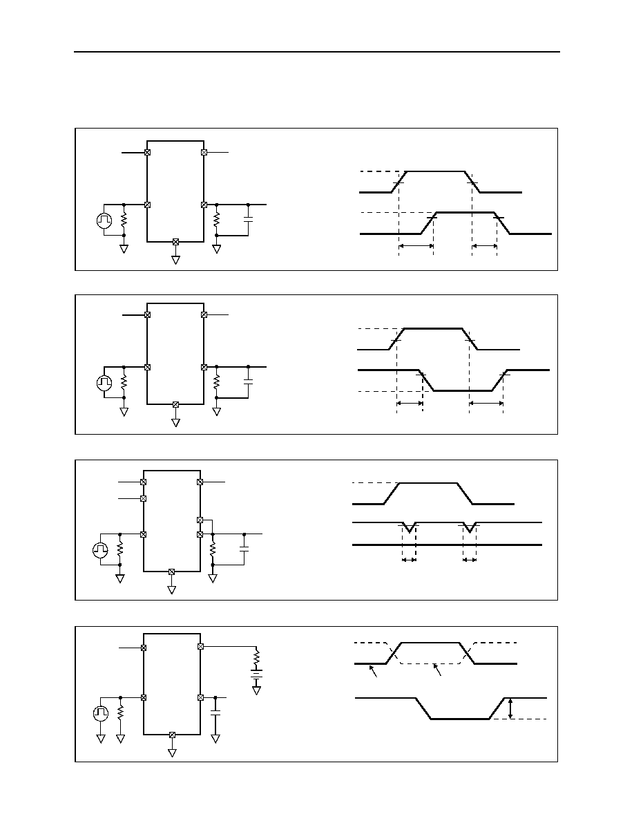
Figure 11. AS1751
/AS1753 Test Circuit and Timing Diagram
Figure 12. AS1752
/AS1753 Test Circuit and Timing Diagram
Figure 13. AS1753
Test Circuit and Timing Diagram
Figure 14. Charge Injection
AS1751/
AS1753
COMx
NOx
35pF
50
V
COMx
INx
V
NOx
50
V+
V+
GND
V
COMx
IN
x
0
0
V
NOx
V
IH
+ 0.5V
t
ON
t
OFF
t
R
< 5ns
t
F
< 5ns
50%
50%
90%
90%
AS1752/
AS1753
COMx
NCx
35pF
50
V
COMx
INx
V
NCx
50
V+
V+
V
COMx
IN
x
0
0
V
NCx
V
IH
+ 0.5V
t
OFF
t
ON
50%
50%
90%
90%
GND
t
R
< 5ns
t
F
< 5ns
AS1753
COM2
NO1
35pF
50
V
COMx
NC2
INx
V
S
V
S
50
V+
V+
V
COMx
IN
x
0
0
V
S
V
IH
+ 0.5V
t
BBM
90%
t
BBM
90%
t
BBM
= t
ON(NOx)
- t
OFF(NCx)
or t
BBM
= t
ON(NCx)
- t
OFF(NOx)
GND
t
R
< 5ns
t
F
< 5ns
COM1
AS175x
COMx
NCx
or
NOx
C
LOAD
1000pF
V
OUT
INx
V
GEN
50
V+
V+
V
IN
0
V+
V
OUT
V
OUT
AS1751
AS1752
V
OUT
is the measured voltage due to charge transfer error Q
when the channel turns off.
Q =
V
OUT x
C
LOAD
GND
R
GEN
V
IN

AS1751, AS1752, AS1753
austria
micro
systems
Data Sheet
Timing Diagrams and Test Setups
www.austriamicrosystems.com
Revision 1.4
10 - 16
Figure 15. NOx, NCx, and COMx Capacitance
Figure 16. Off-Isolation, On-Loss, and Crosstalk
Notes:
1. Measurements are standardized against short-circuit at socket terminals.
2. Off-isolation is measured between COMx and the off NCx/NOx terminal on each switch. Off-isolation = 20log (V
OUT
/
V
IN
).
3. On-loss is measured between COMx and the on NCx/NOx terminal on each switch. On-loss = 20log (V
OUT
/V
IN
).
4. Signal direction through the switch is reversed; worst values are recorded.
AS1751/
AS1752/
AS1753
COMx
NCx or
NOx
INx
V+
V+
As
Required
GND
1MHz
Capacitance
Analyzer
AS1751/
AS1752/
AS1753
COMx
NOx
or
NCx
INx
V+
V+
50
50
50
50
V
IN
V
OUT
0.1µF
Measure
Reference
GND
Network Analyzer
Use 50
termina-
tion for off-isolation
AS1751, AS1752, AS1753
austria
micro
systems
Data Sheet
Pin Assignments
www.austriamicrosystems.com
Revision 1.4
11 - 16
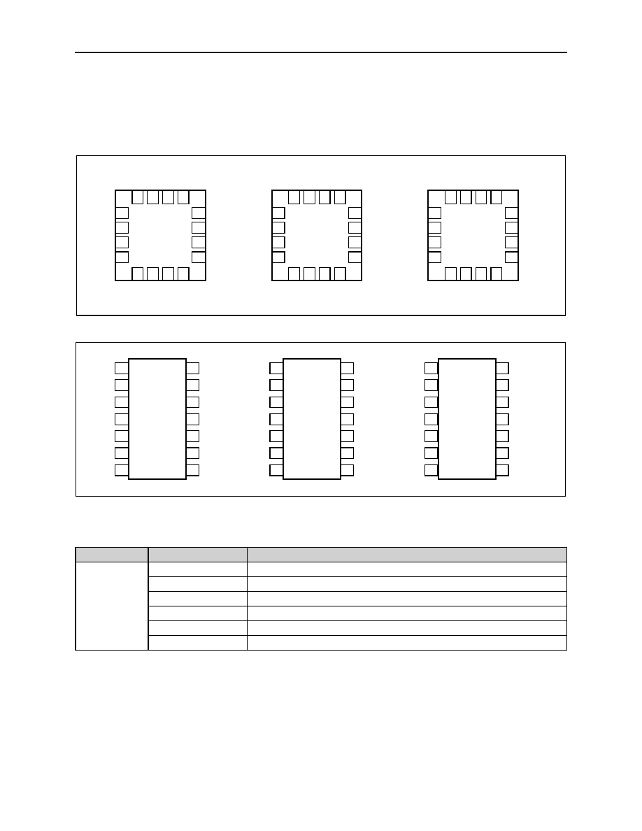
9 Pinout and Packaging
Pin Assignments
Figure 17. QFN Pin Assignments (Top View)
Figure 18. TSSOP Pin Assignments (Top View)
Pin Descriptions
Table 6. Pin Descriptions
Pin Number
Pin Name
Description
(see Figure 17
and Figure 18)
COM1: COM4
Analog Switch 1, 2, 3, 4 Common
GND Ground
IN1:IN4
Analog Switch 1, 2, 3, 4 Logic Control Input
NC1:NC4
Analog Switch 1, 2, 3, 4 Normally Closed Terminal
NO1:NO4
Analog Switch 1, 2, 3, 4 Normally Open Terminal
V+
Input Supply Voltage, +1.6 to +3.6V
15
NO1
AS1753
16
COM1
14
V+
13
IN1
11 NC4
12 IN4
10
≠
9 COM4
6
GND
5
IN3
7
NO3
8
COM3
2
COM2
1
NC2
3
≠
4
IN2
15
NC1
AS1752
16
COM1
14
V+
13
IN1
11 NC4
12 IN4
10
≠
9 COM4
6
GND
5
IN3
7
NC3
8
COM3
2
COM2
1
NC2
3
≠
4
IN2
15
NO1
AS1751
16
COM1
14
V+
13
IN1
11 NO4
12 IN4
10
≠
9 COM4
6
GND
5
IN3
7
NO3
8
COM3
2
COM2
1
NO2
3
≠
4
IN2
AS1751
14 V+
8 NO3
9 COM3
12 IN4
1
NO1
7
GND
6
IN3
3
NO2
11 NO4
4
COM2
10 COM4
5
IN2
13 IN1
2
COM1
AS1752
14 V+
8 NC3
9 COM3
12 IN4
1
NC1
7
GND
6
IN3
3
NC2
11 NC4
4
COM2
10 COM4
5
IN2
13 IN1
2
COM1
AS1753
14 V+
8 NO3
9 COM3
12 IN4
1
NO1
7
GND
6
IN3
3
NC2
11 NC4
4
COM2
10 COM4
5
IN2
13 IN1
2
COM1

AS1751, AS1752, AS1753
austria
micro
systems
Data Sheet
Package Drawings and Markings
www.austriamicrosystems.com
Revision 1.4
12 - 16
Package Drawings and Markings
The devices are available in an 16-pin QFN package and an 14-pin TSSOP package.
Figure 19. 16-pin QFN Package
-C-
A3
A1
SIDE VIEW
PLANE
A
ccc C
0.08 C
11
NX
SEATING
D
D/2
INDEX AREA
E
aaa
C
aaa C
TOP VIEW
2x
2x
4
(D/2 xE/2)
E/2
-B-
-A-
NXL
e
NXb
D2/2
D2
E2/2
2
1
E2
bbb
C A B
ddd
C
-B-
-A-
N N-1
BTM VIEW
6
5
(D/2 xE/2)
INDEX AREA
4
SEE
DETAIL B
SEE
DETAIL B
8
9
Datum A or B
EVEN TERMINAL SIDE
DETAIL B
Terminal Tip
e
e/2
L1
12
5
Common Dimensions
Symbol
Min
Nom
Max
Notes
aaa 0.15
1,
2
bbb 0.10
1,
2
ccc 0.10
1,
2
ddd 0.05
1,
2
A
0.70
0.75
0.80
A1
0.00
0.02
0.05
A3
0.20
Ref
L1
0.03
0.15
D BSC
3.00
1, 2, 10
E BSC
3.00
1, 2, 10
D2
1.30
1.45
1.55
1, 2, 10
E2
1.30
1.45
1.55
1, 2, 10
L
0.30
0.40
0.50
1, 2, 10
N
16
1, 2, 10
ND
4
1, 2, 10
NE
4
1, 2, 10
PIN 1
MARKER

AS1751, AS1752, AS1753
austria
micro
systems
Data Sheet
Package Drawings and Markings
www.austriamicrosystems.com
Revision 1.4
13 - 16
Notes:
1. Dimensioning and tolerancing conform to ASME Y14.5M-1994.
2. All dimensions are in millimeters; angles in degrees.
3. N is the total number of terminals.
4. The terminal #1 identifier and terminal numbering convention shall conform to JEDEC 95 SPP-012. Details of termi-
nal #1 identifier are optional but must be located within the zone indicated. The terminal #1 identifier may be either
a mold or marked feature.
5. Dimension b applies to metallized terminal and is measured between 0.15 and 0.30mm from terminal tip. If one end
of the terminal has the optional radius, the b dimension should not be measured in that radius area.
6. Dimensions ND and NE refer to the number of terminals on each D and E side, respectively.
7. Depopulation is possible in a symmetrical fashion.
8. Figure 19 is shown for illustration only and does not represent any specific variation.
9. All variations may be constructed per Figure 19, however variations may alternately be constructed between square
or rectangle shape per dimensions D and E.
10. Refer to the Dimensions Table for a complete set of dimensions.
11. Bilateral coplanarity zone applies to the exposed heat sink slug as well as the terminals.
12. Depending on the method of lead termination at the edge of the package, pullback (L1) may be present. L minus
L1 to be
0.33mm.
13. For variations with more than one lead count for a given body size and terminal pitch, each lead count for that vari-
ation is denoted by a dash number (e.g., -1 or -2).
14. NJR designates non-JEDEC registered package.

AS1751, AS1752, AS1753
austria
micro
systems
Data Sheet
Package Drawings and Markings
www.austriamicrosystems.com
Revision 1.4
14 - 16
Figure 20. 14-pin TSSOP Package
Notes:
1. All dimensions are in millimeters; angles in degrees.
2. Dimensions and tolerancing per ASME Y14.5M-1994.
3. Dimension D does not include mold flash, protrusions, or gate burrs. Mold flash, protrusions, or gate burrs shall not
exceed 0.15mm per side.
4. Dimension E1 does not include interlead flash or protrusion. Interlead flash or protrusion shall not exceed 0.25mm
per side.
5. Dimension b does not include dambar protrusion. Allowable dambar protrusion shall be 0.08mm total in excess of
dimension b at maximum material condition. Dambar cannot be located on the lower radius of the foot. Minimum
space between protrusion and adjacent lead is 0.07mm for 0.5mm pitch packages.
6. Terminal numbers shown are for reference only.
7. Datums A and B to be determined at datum plane H.
8. Dimensions D and E1 to be determined at datum plane H.
9. This dimension applies only to variations with an even number of leads per side. For variations with an odd number
of leads per package, the center lead must be coincident with the package centerline, datum A.
10. Cross section A-A to be determined at 0.10 to 0.25mm from the leadtip.
Symbol
0.65mm Lead Pitch
1, 2
Note
Symbol
0.65mm Lead Pitch
1, 2
Note
Min
Nom
Max
Min
Nom
Max
A
-
-
1.10
1
0∫
-
8∫
A1
0.05
-
0.15
L1
1.0 Ref
A2
0.85
0.90
0.95
aaa
0.10
L
0.50
0.60
0.75
bbb
0.10
R
0.09
-
-
ccc
0.05
R1
0.09
-
-
ddd
0.20
b
0.19
-
0.30
5
e
0.65 BSC
b1
0.19
0.22
0.25
2
12∫ Ref
c
0.09
-
0.20
3
12∫ Ref
c1
0.09
-
0.16
Variations
D
4.90
5.00
5.10
3, 8
e
0.65 BSC
E1
4.30
4.40
4.50
4, 8
N
14
6
E
6.4 BSC
AS1751, AS1752, AS1753
austria
micro
systems
Data Sheet
www.austriamicrosystems.com
Revision 1.4
15 - 16
10 Ordering Information
The devices are available as the standard products shown in Table 7.
Future Product
Table 7. Ordering Information
Part
Description
Delivery Form
Package
AS1751S
SPST Switch
Tube
14-TSSOP
AS1751S-T
Quad SPST Switch
Tape and Reel
14-TSSOP
AS1751V
Quad SPST Switch
Tray
16-QFN 3mmx3mm
AS1751V-T
Quad SPST Switch
Tape and Reel
16-QFN 3mmx3mm
AS1752S
Quad SPST Switch
Tube
14-TSSOP
AS1752S-T
Quad SPST Switch
Tape and Reel
14-TSSOP
AS1752V
Quad SPST Switch
Tray
16-QFN 3mmx3mm
AS1752V-T
Quad SPST Switch
Tape and Reel
16-QFN 3mmx3mm
AS1753S
Quad SPST Switch
Tube
14-TSSOP
AS1753S-T
Quad SPST Switch
Tape and Reel
14-TSSOP
AS1753V
Quad SPST Switch
Tray
16-QFN 3mmx3mm
AS1753V-T
Quad SPST Switch
Tape and Reel
16-QFN 3mmx3mm

AS1751, AS1752, AS1753
austria
micro
systems
Data Sheet
www.austriamicrosystems.com
Revision 1.4
16 - 16
Copyrights
Copyright © 1997-2005, austriamicrosystems AG, Schloss Premstaetten, 8141 Unterpremstaetten, Austria-Europe.
Trademarks Registered Æ. All rights reserved. The material herein may not be reproduced, adapted, merged, trans-
lated, stored, or used without the prior written consent of the copyright owner.
All products and companies mentioned are trademarks or registered trademarks of their respective companies.
Disclaimer
Devices sold by austriamicrosystems AG are covered by the warranty and patent indemnification provisions appearing
in its Term of Sale. austriamicrosystems AG makes no warranty, express, statutory, implied, or by description regarding
the information set forth herein or regarding the freedom of the described devices from patent infringement. austriami-
crosystems AG reserves the right to change specifications and prices at any time and without notice. Therefore, prior
to designing this product into a system, it is necessary to check with austriamicrosystems AG for current information.
This product is intended for use in normal commercial applications. Applications requiring extended temperature
range, unusual environmental requirements, or high reliability applications, such as military, medical life-support or life-
sustaining equipment are specifically not recommended without additional processing by austriamicrosystems AG for
each application.
The information furnished here by austriamicrosystems AG is believed to be correct and accurate. However,
austriamicrosystems AG shall not be liable to recipient or any third party for any damages, including but not limited to
personal injury, property damage, loss of profits, loss of use, interruption of business or indirect, special, incidental or
consequential damages, of any kind, in connection with or arising out of the furnishing, performance or use of the tech-
nical data herein. No obligation or liability to recipient or any third party shall arise or flow out of
austriamicrosystems AG rendering of technical or other services.
Contact Information
Headquarters
austriamicrosystems AG
A-8141 Schloss Premstaetten, Austria
Tel: +43 (0) 3136 500 0
Fax: +43 (0) 3136 525 01
e-mail:
info@austriamicrosystems.com
For Sales Offices, Distributors and Representatives, please visit:
http://www.austriamicrosystems.com
austria
micro
systems
≠ a leap ahead