Revision 2.1
Page 1 of 12
austria
micro
systems
Key Features
-
Analog line interface and speech circuit for a/b terminals
on a 28-pin CMOS-IC
-
2 balanced transmit inputs
-
3 unbalanced transmit inputs
-
2 buffered single ended receive outputs (R
L
>150
)
-
1 auxiliary single ended receive output (R
L
>10k
)
-
Low noise (max. -72dBmp)
-
Soft clipping to avoid harsh distortion
-
Operating range from 15mA to 100mA (down to 5mA
with reduced performance)
-
Line loss compensation selectable by pin option
-
Real and complex impedance selectable by external
components
-
Side tone adaptation selectable by external components
-
Digital controls input for mode selection
-
Rx volume control
General Description
AS2504 is a CMOS integrated circuit that incorporates DC
and AC line adaptation (DC-mask and synthesized AC-
impedance of 1000
) as well as a speech circuit with
softclipping, line loss compensation and Rx-volume control.
It shall act as an a/b-line powered or auxiliary powered
device, which is controlled by a CPU.
Applications
Cordless base stations, answering machines, a/b-line or
auxiliary powered telephone sets.
Package
Available in 28 pin SOIC
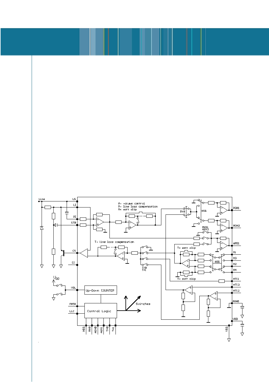
Block Diagram
Cordless telephone,
answering machine line interface
AS2504
DATA SHEET
Data Sheet AS2504
austria
micro
systems
Revision 2.1
Page 2 of 12
Pin description
Pin #
Symbol
Function
7
LS
L
ine Current
S
ense Input
Input for sensing the line current
5
LI
L
ine
I
nput
Input used for power extraction and line current sensing
6
RI
R
eceive
I
nput
Input for ac-separated receive signal
13
STB
S
ide
T
one
B
alance Input
Input for side tone cancellation network
3
CS
C
urrent
S
hunt Control Output
N-channel open drain output to control the external high power shunt transistor for
synthesizing AC- and DC-impedance, modulation of line voltage and shorting the line during
make periods of pulse dialing
14
CI
C
omplex
I
mpedance Input
Input pin for the capacitor to program a complex impedance
25
MASK
MASK
Input pin to set circuit into power down mode during e.g. LD-dialing. During MASK=HIGH, CS-
pin is internally shorted to ground.
26
LLC
L
ine
L
oss
C
ompensation Select Pin
45mA-75mA
--> VDD
20mA-50mA
--> AGND
None
--> VSS
11
VDD
V
oltage
D
rain
D
rain
Positive Power Supply, for external circuitry t.m. 4.0mA@I
L
=20mA and 4.0mA@I
L
=20mA
4
VSS
V
oltage
S
ource
S
ource
Negative Power Supply
12
AGND
Analog
G
round
Special ground for the internal amplifiers
2
M1
M
icrophone Input
1
Differential input for the microphone (electret)
1
M2
M
icrophone Input
2
Differential input for the microphone (electret)
28
M3
M
icrophone Input
3
Differential input for the microphone (electret)
27
M4
M
icrophone Input
4
Differential input for the microphone (electret)

Data Sheet AS2504
austria
micro
systems
Revision 2.1
Page 3 of 12
Pin #
Symbol
Function
24
ATI1
A
uxiliary
T
ransmit
I
nput
1
R
I
>= 25k
23
ATI2
A
uxiliary
T
ransmit
I
nput
2
R
I
>= 100k
15
ATI3
A
uxiliary
T
ransmit
I
nput
3
R
I
>= 100k
8
ROH1
R
eceive
O
utput to
H
andset
1
Output for driving a dynamic earpiece with an impedance from 150
to 300
(max. 0.7Vp)
9
ROH2
R
eceive
O
utput to
H
andset
2
Output for driving a dynamic earpiece with an impedance from 150
to 300
(max. 1.4Vp)
10
ARO1
A
uxiliary
R
eceive
O
utput
1
R
L
> 10k
(max. 1.4Vp)
16
VOL
VOL
ume
Input pin for increasing (= connect to V
IN
>= V
DD
-0.3V) or decreasing (= connect to V
IN
<=
VSS+0.3V) the Rx volume. The idle state is between V
SS
+1.4V < V
IN
< V
DD
-1.4V. Max rise
time 50ns, max fall time 50ns, min pulse width 1us
22
HSS
H
and
S
et or Head
S
et / bit
Digital input to select the ROH1 or ROH2 signal output path
21
RX0
R
eceive
0
/ bit
Digital input to select a signal path
18
AUX0
A
uxiliary
0
/ bit
Digital input to select a signal path
17
AUX1
A
uxiliary
1
/ bit
Digital input to select a signal path
20
TX0
T
ransmit
0
/ bit
Digital input to select a signal path
19
TX1
T
ransmit
1
/ bit
Digital input to select a signal path
Data Sheet AS2504
austria
micro
systems
Revision 2.1
Page 4 of 12
Functional Description
Modes of operation
There are three possible modes:
Idle Mode: AS2504 is disconnected from the a/b-line (= no
line current) and VDD is not supplied by auxiliary power. All
internal circuits are powered down. Input of digital control
signals is not possible.
Line Power Mode: AS2504 is connected to the a/b-line and
VDD is generated by the internal power extraction. The
speech circuit is powered up. The line interface circuit is
functional (DC-mask and AC-impedance are synthesized).
Input of digital control signals is possible.
Aux. Power Mode: AS2504 is disconnected from the a/b-line
(= no line current) and VDD is supplied by auxiliary power.
The speech circuit is powered up. The line interface circuit
is not functional (DC-mask and AC-impedance). Input of
digital control signals is possible.
Start-up in Line Power Mode
As soon as AS2504 is supplied with line current, the
external V
dd
capacitor will be charged up via the LI- and
VDD-pin. After the V
dd
voltage has reached the operating
level of 2V, the line interface circuit and the selected signal
path of the speech circuit is switched on. This off-hook
status is signaled to the internal logic via the LS-pin
(voltage level sensitive).
Start-up in Aux. Power Mode
As soon as AS2504 is supplied with auxiliary power at the
VDD-pin, the selected signal path of the speech circuit is
switched on. The line interface circuit (DC-mask and AC-
impedance) is not functional. This on-hook status is
signaled to the internal logic via the LS-pin (voltage level
sensitive).
DC conditions
The normal operating mode is from 15mA to 100mA. An
operating mode with reduced performance is from 5mA to
15mA. In the line hold range from 0mA to 5mA the device is
in a power down mode and the voltage at LI is reduced to a
maximum of 3.5V.
The DC characteristic is determined by the voltage at LI-pin
and a 30
resistor between LI- and LS-pin. It can be
calculated by the following equation: V
LS
= V
LI
+ I
Line
*
30
. The t.m. voltage at the LI-pin is 4.5V. The calculation
leads to the following DC resistances: 330
to 75
at line
currents from 15mA to 100mA.
With a HIGH at the MASK-pin, the speech circuit and other
parts of the device, which are not needed for operation, are
in power down mode in order to save current. The CS-pin is
pulled to V
ss
to turn the external shunt transistor fully on.
This guarantees a low voltage drop (<1V) at the LI-pin
during make periods of pulse dialing or flash.
2/4 wire conversion
AS2504 has a built-in dual Wheatstone bridge with one
common ground. This provides a maximum of independence
of AC-impedance and side tone from each other. One can
adapt side tone without changing the AC-impedance.
AC-impedance
The AC-impedance of AS2504 is set to t.m. 1000
. With
the external capacitor at CI-pin it can be programmed
complex. With an external resistor of approx. 1.5k
connected to the LS-pin it can be programmed to 600
.
Z
AC(syn)
= 33 * 30
.
Side Tone
A good sidetone cancellation can be achieved by using the
following equation:
Z
BAL
/Z
LINE
= 10
Transmit path
The gain of the M1/M2
LS is set to 37dB. The input is
differential with an impedance of 20k
. The soft clip circuit
limits the output voltage at LS to 2V
p.
The attack time is
30�s/6dB and the decay time is 20ms/6dB.
The gain of the M3/M4
LS is set to 43dB. The input is
differential with an impedance of 10k
. The soft clip circuit
limits the output voltage at LS to 2V
p.
The attack time is
30�s/6dB and the decay time is 20ms/6dB.

Data Sheet AS2504
austria
micro
systems
Revision 2.1
Page 5 of 12
The gain of the ATI1
LS is set to 6dB. The input is
unbalanced with an impedance of 25k
. There is no
softclipping.
The gain of the ATI2
LS is set to 20dB. The input is
unbalanced with an impedance of 100k
. There is no
softclipping.
Intercom path
The gain of the ATI3
ROH1 is set to 6dB. The input is
unbalanced with an impedance of 100k
. There is no
softclipping.
The gain of the ATI3
ROH2 is set to 12dB. The input is
unbalanced with an impedance of 100k
. There is no
softclipping.
The gain of the M1/M2
ARO1 is set to 23dB. The input is
differential with an impedance of 20k
. The soft clip circuit
limits the output voltage at ARO1 to 0.4V
p.
The attack time
is 30�s/6dB and the decay time is 20ms/6dB.
The gain of the M3/M4
ARO1 is set to 29dB. The input is
differential with an impedance of 10k
. The soft clip circuit
limits the output voltage at ARO1 to 0.4V
p.
The attack time
is 30�s/6dB and the decay time is 20ms/6dB.
Receive path
The gain of the LS
ROH1 receive path is set to 3dB. The
receive input is the differential signal of RI and STB. The
soft clip circuit limits the output voltage at ROH1 to 0.7V
p.
It
prevents harsh distortion and acoustic shock. There is
volume control and LLC for this path.
The gain of the LS
ROH2 receive path is set to 9dB. The
receive input is the differential signal of RI and STB. The
soft clip circuit limits the output voltage at ROH2 to 1.4V
p.
It
prevents harsh distortion and acoustic shock. There is
volume control and LLC for this path.
The gain of the LS
ARO1 receive path is set to 3dB. The
receive input is the differential signal of RI and STB. There
is no softclipping, no LLC and no volume control for this
path.
Rx volume control
The volume control is available for LS
ROH1 and LS
ROH2. It can be decreased by 6dB and increased by 8dB in
2dB steps from the default levels as described in the last
paragraph. It remains in the pre-set position as long as VDD
does not decrease less than 2.2V.
Line Loss Compensation
The line loss compensation is a pin option. When it is
activated, the transmit and receive gains for both I/O's are
decreased by 6dB at line currents from 20mA to 50mA when
the LLC-pin is connected to AGND and from 45mA to 75mA
when the LLC-pin is connected to VDD. The line loss
compensation is deactivated when LLC-pin is connected to
VSS.
Digital interface
The selection of the available signal paths must be set via
the digital control pins. The following modes are possible:
HSS: bit
RX0: bit
0
0
LS
ROH1
1
0
LS
ROH2
0
1
ATI3
ROH1
1
1
ATI3
ROH2
AUX0: bit
AUX1: bit
HSS: bit
1
1
X
MUTE
0
1
0
M1/M2
ARO1
0
1
1
M3/M4
ARO1
1
0
X
LS
ARO1
0
0
X
MUTE
TX0: bit
TX1: bit
HSS: bit
0
0
0
M1/M2
LS
0
0
1
M3/M4
LS
0
1
X
ATI1
LS
1
0
X
ATI2
LS
1
1
X
MUTE