 | –≠–ª–µ–∫—Ç—Ä–æ–Ω–Ω—ã–π –∫–æ–º–ø–æ–Ω–µ–Ω—Ç: AS8846 | –°–∫–∞—á–∞—Ç—å:  PDF PDF  ZIP ZIP |

Data Sheet AS8446
Revision 1.8, Date 2005-03-17
Page 1 of 35
Vbat
M
Rm
e
a
s
A
S
8446
TP
Wake-up
Vbat
VSS
Iref
VDDctrl
VDD
CP2
CP1
Vpump
OUT
CS
CMP
DATAout
CMN
FAIL
PWM
25
26
24
23
22
21
20
19
18
17
16
CLK
DATAin
Test1
Test2
27
28
RESET
1
D1
Cbat
Tr1
CP12
CP0
VDD = 5 V
CV
D
D
Rref
R
NTC
R
T1
M+
M-
GND_P
Power part
Control part
W
akeUp
15
2
3
4
5
6
7
8
9
10
11
12
13
14
VMO
ADC
WD
µP
Q1
OSC1
OSC2
PWMout
VDD
GND
(optional)
Test3
n.c.
CLK
CS
INR
ANA
Port1
Port2
SPIout
SPIin
RESET
Tout
GND_P
VSS
Key Features
-
Programmable PWM DC Motor Driver / Controller with µP
Interface (Three Wire Interface)
-
Programmable Functions and Parameters for Motor
Current, Voltage and Speed Regulation
-
Single Voltage Supply in the range
Vbat = 6.0 V to 18 V (Vbat,max = 30 V)
1
-
Total Power Efficiency up to 96 %
-
Low RF Emission within the whole frequency range due to
an integrated special EMC optimized driver
-
Dynamically self-adjusting slew rate regulated switching
technology
-
Fully protected by programmable failure handling
procedures via µP
-
Fast Over Current and Over / Under Voltage Detection
and Protection, Battery Voltage Monitoring
-
External and On Chip Temperature Detection and
Protection
-
Motor Current and Speed Measurement with a shunt
resistor and capability of trimming the chip for an external
shunt value
-
Programmable Parameters:
∑
EMC compliant Driver Functions
∑
Over Current, Over / Under Voltage
Threshold Values
∑
Motor Failure Threshold Levels
∑
Motor Current Measurement Range
∑
Trimming for the current measurement shunt
∑
PWM Frequency, Charge Pump Monitor
-
Charge Pump to control high side drivers
-
Integrated 5 V Power Supply for external components
(µP, etc.)
-
Standby and Wake-up capability
-
Sleep / Wake-up Mode system controlled by the
µ
P and
the Wake-up Pin
-
SOIC 28 Package
General Description
The AS8446 is a complete and fully protected PWM DC motor
driver/controller, which can be implemented by interfacing a
low cost 8-bit
µ
P and a high-side N-channel power FET
switch.
1
Low-Batttery-mode between 6.0 V and 6.5 V
It is an advanced PWM DC motor controller subsystem with
an excellent EMC behavior targeted especially for high
current automotive applications. The optimization of the EMC
behavior of the entire module only by software changes
makes it easier to implement it in harsh environments.
The programmability of parameters and functions allows the
adaptation of the AS8446 to a wide range of applications.
So the system can act either as a motor current or motor
speed or motor voltage regulator. Also a full diagnosis of
motor failures and power FET failures, over temperature and
over/under voltage can be formed by programmable failure
handling procedures using the motor characteristic and the
real time measured motor current, motor speed and battery
voltage.
Applications
-
Fan cooler
-
Air conditioning
-
Fuel pumps
-
Water and oil pumps
-
General purpose DC Motor Regulators
Typical Application Diagram
AS 8446
Programmable PWM DC Motor Driver / Controller
DATA SHEET

Data Sheet AS8446
Revision 1.8, Date 2005-03-17
Page 2 of 35
Functional Description
Overview
The AS8446 is a complex integrated circuit, which contains
both low and high voltage circuitry to regulate PWM brush DC
motors with an external n-channel power FET and an
8-bit
µP. The regulation loop is a closed loop environment
where a
µP is connected to the device with a Three-Wire
Interface. The AS8446 measures and delivers the motor
current as an analog value to the
µP. The µP uses a special
algorithm to calculate the motor speed by considering the
motor current as a function of time. This technique allows the
system to act either as a motor current or a motor speed
regulator. The AS8446 also monitors and delivers the battery
voltage to the
µP as an analog value and by leveraging this
voltage-monitoring feature a motor voltage regulator could
be implemented also. A full diagnosis of motor and power FET
failures is performed automatically by the programmable
failure handling functions after carefully analyzing the motor
characteristics, real-time motor current, motor speed and
battery voltage.
The dynamically self-adjusting slew rate regulated switching
technology (patented) is one of the most important features of
this ASSP in automotive applications. This technology
enables two features of the PWM DC motor regulator, which
were up till now impossible to realize:
∑
Excellent EMC behavior (very low RF emission in the
whole frequency range)
∑
High power efficiency up to 96 % @ f
PWM
= 20 kHz
(fall / rise time down up to < 150 ns)
Most of the parameters (e.g. PWM frequency, slew rate, over
current threshold, current measurement range, etc.) of the
AS8446 can be programmed (setting up the internal registers)
through the Three-Wire Interface, which makes the regulator
a versatile and easily adaptable device to a wide range of
regulation modes and motors.
The field programmability option of the slew rate regulation
parameters makes it easier to comply with the system level
EMC behavior (regulator board, motor, power cables, etc.)
A bandgap is used as a reference for a Low Drop Voltage
Regulator with a nominal output voltage of 5 V.
This regulator is capable to deliver a supply current of up to
40 mA. Higher current is possible with an external bipolar
transistor.
The device is bundled with a set of software to handle the
regulation loop, motor speed measurement and failure
detection. A sleep/wake up system is integrated to bring the
AS8446 into a power save mode. It is controlled via the
specified wake-up pin.
A short overview of the main features follows.
∑
programmable PWM DC motor current, speed or voltage
regulator
∑
single voltage supply in the range Vbat = 6.0V to 18V
(Vbat,max = 30 V)
∑
Low-Battery-Mode guarantees operation also when
battery voltage is between 6.0V and 6.5V; In this mode
the output driver is constantly on (100% PWM),
Vpump-Vbat
4.0V.
∑
applicable directly to the automotive battery supply
(burst, surge, load dump)
∑
closed loop regulation of the motor speed, motor current
or motor voltage with a
µP.
∑
high power efficiency of the whole regulator module (up
to 96 % @ f
PWM
= 20 kHz)
∑
low RF emission within the whole frequency range
∑
fully protected by programmable failure handling
procedures (see below: Security Functions)
∑
fast over current and over / under voltage detection and
protection
∑
motor current and motor speed measurement with only
one shunt resistor (typ. measurement voltage at nominal
motor current: 50 mV)
∑
on chip trimming capability of the external shunt resistor
∑
Sleep/wake up mode system controlled by the
µP and
the wake-up pin
∑
Three Wire Interface
∑
programming possibilities of the following regulator
parameters inside of the AS8446:
-
PWM frequency (generated by
µP, e.g. 20 kHz)
-
charge pump voltage monitoring and protection
-
slew rate control parameters (EMC behavior)
-
power FET Gate driver currents up to 500 mA
-
over current threshold level
-
over / under voltage threshold level
-
motor current measurement range and trimming of
the external current measurement resistor
∑
programming possibilities of the following regulator
parameters / functions via the
µP
-
motor failure threshold levels (motor currents and
voltages) for all motor failures: blocked motor, open
wire, no load, shorted motor segments, etc.
-
failure handling procedures for all motor failures,
over / under voltage and for over temperature (type
of reaction and timing)
-
sleep mode criteria and sleep mode signal to the
AS8446

Data Sheet AS8446
Revision 1.8, Date 2005-03-17
Page 3 of 35
-
closed loop regulation timing with
µP for speed,
current and voltage control
-
special features e.g. suppression of particular motor
speeds, dynamical change of the over current
threshold level, etc.
Security Functions
Extensive diagnosis of the DC motor and the power FET as
well as failure handling procedures are programmable via a
µP.
∑
over current detection and protection
∑
no load detection of the motor
∑
open wire detection (motor or power switch)
∑
short circuit of the power switch detection
∑
blocked motor detection and protection
∑
short circuited motor segments detection and protection
∑
protection of the power FET and the AS8446, if the
motor works in generator mode
∑
battery voltage monitoring and over / under voltage
detection and protection
∑
two over temperature detection and protection modes
-
external temperature sensor
-
on chip temperature sensor
Item (Start up values)
AS 8446
Over Voltage Threshold
40.0 V
Under Voltage Threshold
2.5 V
Minimum Charge Pump Voltage
4.0 V
Over Current Threshold (Shunt
Measurement Voltage)
125 mV
Mode after Start up
sleep
mode
Table 1
Start up values of the AS 8446

Data Sheet AS8446
Revision 1.8, Date 2005-03-17
Page 4 of 35
Pin Description
The AS8446 Motor Driver/Controller contains the
driver/controller chip in a SOIC28 package
The complete PWM DC Motor Regulator board needs an
additional
µP to close the regulation loop and control the
whole regulator (dual package solution, free choice of the
controlling
µP).
Pinout AS8446
Figure 1
Pinout AS 8446
Pin Description AS8446, Pin Types
S
... power supply
AI
... analog in
AO
... analog out
AIO
... analog in/out
DI
... digital in
DIPU
... digital in with pull-up
DIPD
... digital in with pull-down
DO
... digital out
DIO
... digital in/out
DO_T
... digital out, tristate
LV
... low voltage
HV
... high voltage
Pin Name
Type
Note
1
CMN
HV AI
Current Measurement Input
(negative side)
2
CMP
HV AI
Current Measurement Input
(positive side)
3
VMO
HV AI
Motor Voltage Input
4
Vbat
S
Battery Voltage, Main Supply
5
TP
HV AI
Temperature Sensor Input
6
FAIL
LV DO
Error Status Output of
AS8446
7
CS
LV DIPU
Chip Select, Enable Pin of
Three Wire Interface
8
ADC
HV AO
Analog Measurement Output
(multiplexed)
9
Wake-up HV AIO
Wake-up Pin
10
n.c.
11
Tst 1
LV DIPU
Test Pin 1 (1)
12
Tst 2
LV DO
Test Pin 2 (2)
13
DATAin
LV DIPD
Data Input of the Three-Wire
Interface
14
DATAout LV DO_T Data Output of the Three-
Wire Interface
15
Clk
LV DIPD
Clock of the Three-Wire
Interface
16
PWM
LV DIPU
PWM Input (Control of the
Power FET Driver)
17
Tst 3
LV DO
Test Pin 3 (2)
18
WD
LV DIPU
Watch Dog Input
19
RESET
LV DO
Reset Output (controlled by
Watch Dog)
20
Iref
LV AIO
Reference Current Pin
21
VDD
AI
VDD feedback input
22
VDDctrl
HV AO
VDD supply (5 V generated
by the on chip voltage
regulator)
23
CP1
HV AIO
Charge Pump Capacitor (Vbat
side)
24
CP2
HV AIO
Charge Pump Capacitor
(Vpump side)
25
Vpump
AO
Charge Pump Buffer
Capacitor
26
OUT
HV AO
Power FET Driver Output
27
GND_P
S
Power Ground
28
VSS
S
Digital/Analog Ground
Table 2
PIN description of AS 8446
Note (1) Must be connected to VDD
Note (2) Must be left open
A
S
8446
TP
Wake-Up
Vbat
VSS
Iref
VDDctrl
VDD
CP2
CP1
Vpump
OUT
GND_P
CS
CMP
DATAout
CMN
FAIL
PWM
25
26
24
23
22
21
20
19
18
17
16
Clk
DATAin
Tst 1
Tst 2
27
28
RESET
1
15
2
3
4
5
6
7
8
9
10
11
12
13
14
VMO
ADC
WD
Tst 3
n.c.

Data Sheet AS8446
Revision 1.8, Date 2005-03-17
Page 5 of 35
Block Diagram
Figure 2
Block Diagram of AS8446
10
V
Ch
a
r
g
e
p
u
m
p
GND
M
o
to
rc
u
r
re
n
ta
n
d
s
p
e
ed
me
a
s
u
re
m
e
n
t
/
o
v
e
r
c
u
r
r
e
nt
sle
wr
ate
(hig
h)
pro
gra
mming
M
o
to
r
-
a
nd
P
o
we
r
F
E
T
p
r
ot
ec
t
i
on
Cl
k
V
DDH
=
V
b
a
t
M
OUT
Se
r
ia
l
In
t
e
r
f
a
c
e
DA
T
A
i
n
R/
W
Co
n
t
r
o
l
S
hi
f
t
Re
g
i
s
t
er
AS
8
4
44
uP
b
a
se
dD
CM
o
to
r
R
eg
u
l
a
t
or
Bi
t
_
0
B
it
_n
R
CO
sc
i
ll
a
t
o
r
50
k
Hz
CP
1
CP
2
V
p
u
m
p
P
WM
VD
D
H
21
2
Rme
as
V
A
_c
u
r
re
n
t
=k
x
*I
m
o
to
r
A
_cu
r
r
e
n
t
CM
p
C
M
n
W
a
k
e
-u
p
In
t
er
f
a
c
e
Ts
t
1
Re
g
i
s
t
e
r
s
SE
T
_
0
a
)s
et
t
i
n
g
s
b
)c
o
n
tr
o
l
SE
T_
k
3
PW
M
TP
V
DDH
1
P
o
ver
c
12
sl
e
e
p
CLK
p
u
m
p
V
DD
H
pr
o
g
r
a
mm
i
n
g
an
d
t
ri
mm
i
ng
(o
v
e
r
c
u
r
r
en
t,
Rm
e
a
s
)
GN
D
_
P
DA
T
A
o
u
t
CS
ADC
A_
o
ve
rc
k
5
k
6,
k
7
P
T
o
ve
r
2
FA
I
L
Ts
t
2
pr
og
ra
m
m
a
b
le
:
12
V
,
2
4
V
,
4
2
V
Vo
lt
a
ge
Mo
ni
t
o
ri
n
g
Vi
n
=
V
b
a
t
progr
amming
(a
n
a
l
o
g
)
VS
SA
5V
-
r
e
g
u
l
a
tor
(
b
an
dg
a
pr
ef
.
)
VD
D
VD
D
c
t
r
l
VD
D
V
DDH
ba
nd
g
a
p
re
fe
re
nc
e
Vr
e
f
/I
r
e
f
ge
n
er
a
t
or
Vre
f
Ire
f
Vr
e
f
=
1
.
0V
Vbat
_
m
on
pa
c
ka
g
e:
SO
IC
2
8
V
DDc
t
r
l
au
st
r
i
a
mi
c
r
o
sy
st
e
m
s
Vr
e
f
T
2
On
c
h
i
p
O
v
e
r
Te
m
p
e
r
a
t
u
r
e
det
e
ct
i
o
n
Vr
e
f
T1
Ex
t
e
r
n
a
l
O
v
e
r
Te
m
p
e
r
a
t
u
r
e
de
t
e
c
t
i
o
n
PW
M
H
V-
IN
/
LV
-
O
U
T
V
DDH
=
V
b
a
t
PO
R
PO
R
t
S
l
ee
p
/w
a
k
e
u
ps
y
s
t
e
m
V
DD
p
d
Vr
e
f
V
P
V
o
ve
r
P
Vu
n
de
r
P
To
ve
r
1
Po
v
e
r
c
OR
RES
E
T
3
C
P1
2
CP
0
C
V
DD
Rre
f
V
DD
R
T1
RNT
C
Rx
sl
e
e
p
WD
V
A
_o
v
e
r
c
=k
y
*
I
m
o
t
o
r
Self
Ad
justing
Sle
wR
ate
Re
gul
atio
n
In
terf
ace/
Contr
ol
Hi
g
h
S
i
d
e
Dr
i
v
e
Lo
w
S
id
e
D
ri
ve
sle
wr
ate
(low)
prog
ra
mming
Imo
to
r
lo
w
v
o
l
t
a
g
e
hi
g
h
v
o
l
t
a
ge
Wa
t
c
h
d
og
Ir
e
f
Vm
o
VD
D
OR
VS
S
a
c
t
i
ve
/
d
e
ac
t
i
v
e
Cl
k
_w
d
wd
Analog
MUX
2
T
P
A
_
cu
rr
en
t
A_
o
v
e
r
c
V
b
a
t_
m
on
W
a
ke-
u
p
Ts
t
3

Data Sheet AS8446
Revision 1.8, Date 2005-03-17
Page 6 of 35
General Application Diagram
Vbat
M
Rm
e
a
s
A
S
8
446
TP
Wake-up
Vbat
VSS
Iref
VDDctrl
VDD
CP2
CP1
Vpump
OUT
CS
CMP
DATAout
CMN
FAIL
PWM
25
26
24
23
22
21
20
19
18
17
16
CLK
DATAin
Tst1
Tst2
27
28
RESET
1
D1
Cbat
Tr1
CP12
CP0
VDD = 5 V
CV
DD
Rref
R
NTC
R
T1
M+
M-
GND_P
Power part
Control part
Wak
e
Up
15
2
3
4
5
6
7
8
9
10
11
12
13
14
VMO
ADC
WD
µP
Q1
OSC1
OSC2
PWMout
VDD
GND
(optional)
Tst3
n.c.
CLK
CS
INR
ANA
Port1
Port2
SPIout
SPIin
RESET
Tout
GND_P
VSS
Figure 3
General Board Diagram of a complete PWM DC Motor Regulator
Remarks:
a)
The communication between the AS8446 and the controlling
µP is realized via the Three-Wire Interface
b)
The communication of the whole motor regulator module with the environment can be realized in different ways:
1. low voltage 5 V digital input using a digital
µP port
2. low voltage 5 V analog output using an analog ADC input of the
µP
c)
The EMC parameters to optimize the EMC behavior of the whole regulator system can be stored in the program of the
µP
and transmitted to the AS8446 via Three-Wire Interface during start up of the system.
d)
The customer has free choice of the
µP.

Data Sheet AS8446
Revision 1.8, Date 2005-03-17
Page 7 of 35
Absolute Maximum Ratings (NON OPERATING)
Stresses beyond those listed under Absolute Maximum Ratings may cause permanent damage to the device. These are stress
ratings only. Functional operation of the device at these or any other conditions beyond those indicated under Operating
Conditions is not implied. Exposure to absolute maximum rating conditions for extended periods may affect device reliability.
Parameter
Symbol
Min
Max
Unit Note
Battery voltage
Vbat
-0.3
30
V
(1)
Pumped voltage
Vpump
-0.3
44
V
Low Power Supply Voltage
VDD
-0.3
7
V
Input Pin Voltage (Low voltage pins)
Vin
-0.3
VDD+0.3
V
Input Current (latchup immunity)
Iscr
-100
100
mA
125∞C
ESD
-0,9
0,9
kV
Norm: MIL 883 E method 3015 (2)
Total Power dissipation
Pvtot
500
mW
Junction temperature
Tj
150
∞C
Storage temperature
Tstg
-55
150
∞C
Humidity
5
85
%
Non condensing
Body temperature
TBody
240
∞C
Norm: IPC/JEDEC J-STD 020 C
Note (1): Load Dump, 500ms, according to DIN40839
Note (2): Except for Pin 1 (CMN) and Pin 25 (Vpump): ESD = +/- 0,5 kV
Table 3
Absolute Maximum Ratings
Operating Conditions
Parameter
Symbol
Min
Typ
Max
Unit
Note
Battery voltage (normal
operating-mode)
Vbat
6.5
18
V
(1)
Battery voltage (Low-Battery-
mode)
Vbat
6.0
6.5
V
Vpump-Vbat
4.0V;
Vout = const. high; (2)
Pumped voltage
Vpump
Vbat + 4V
Vbat + 10V
Vbat + 14V
V
(2)
Low Voltage Power Supply
VDD
4.8
5.15
V
(2);(3)
Standby Current (power down)
I_pd1
Vbat
(50)
µA
Tamb < 27
∞
C; (4)
Standby Current (power down)
I_pd2
Vbat
90
µA
Tamb < 125
∞
C;
Vbat = 13.5V
Ambient temperature
Tamb
-40
125
∞
C
Note (1): Jump Start: Vbat < 28V, 1 min, 1 pulse/h
Note (2): Low Battery mode guarantees operation when the battery voltage is below 6.5V; In this mode the output driver is
constantly on (100% PWM), Vpump-Vbat
4.0V at 250µA load on Pin OUT; the load current of VDD is limited to 2.5mA
Note (3): Low Drop voltage regulator; 40 mA max. external load at VDD; higher current with external transistor possible
Note (4): only as information. Will not be tested
Table 4
Operating Conditions
Thermal Characteristics
Parameter
Symbol
Min
Max
Unit Note
Thermal resistance from junction to ambient
Rth,ja
76.2
∞C/W free air, single layer PCB
Table 5
Thermal Characteristic

Data Sheet AS8446
Revision 1.8, Date 2005-03-17
Page 8 of 35
Characteristics for Analog and Digital Inputs and Outputs
CMOS LV Digital Input
Pins: Clk, DATAin, CS, PWM, WD
Parameter
Symbol
Min
Max
Unit Note
High Level Input Voltage
VIH
0.7 * VDD
V
Low Level Input Voltage
VIL
0.3 * VDD
V
Input Leakage Current
ILEAK
-1
1
µA
pull-up/down current for inputs with
pull-up/down typ. 60µA
Table 6
CMOS Input parameters
CMOS LV Digital Output
Pins: RESET, DATAout, FAIL
Parameter
Symbol
Min
Max
Unit Note
High Level Output Voltage
VOH
VDD -0.5
V
C
LOAD
= 50 pF
Low Level Output Voltage
VOL
VSS +0.4
V
C
LOAD
= 50 pF
Table 7
CMOS Output parameters
Analog Signals Input / Output
Pins: Vpump, CP1, CP2, OUT, CMP, CMN, VMO, ADC, TP, Iref
Parameter, Pin Name
Pin type
Symbol
Min
Typ
Max
Unit Note
Charge Pump Voltage, pin: Vpump
HV S
Vpump
Vbat + 6
Vbat + 4
Vbat
+ 10
Vbat + 14
V
(1)
Charge pump switched capacitor
voltage, pin: CP1
HV AIO
V
CP1
VSS
Vbat
V
Charge pump switched capacitor
voltage, pin: CP2
HV AIO
V
CP2
VSS
Vbat + 14
V
HS driver source current, pin: OUT
HV AO
Iout_p
-500
mA
(2)
HS driver sink current, pin: OUT
HV AO
Iout_n
500
mA
(2)
Motor current measurement inputs,
Common mode range, pins: CMP, CMN
HV AI
V
CMP,
V
CMN
-1.5
Vbat
V
Motor voltage input, pin: VMO
HV AI
V
VMO
-1.5
Vbat
V
Analog measurement output voltage,
pin: ADC
LV AO
V
A_current
0
VDD
V
Multiplexed analog
output (3)
External temperature sensor input,
threshold voltage, pin: TP
LV AI
V
TP_th
0
0.5
VDD
VDD
V
Threshold voltage:
VDD / 2
Reference current generation voltage,
pin: Iref
LV AI
Vref
1.0
V
(4)
Note (1):
external capacitors CP1/2 = 100 nF, CP0 = 400 nF recommended;
on chip Vpump monitoring and protection: Vpump_min = (Vbat + 6 V) or (Vbat + 4 V), programmable
Note (2):
typical rise/ fall time at the external Power MOSFET source: 0.2 µs to 0.5 µs,
independently programmable rise and fall times, voltage range of the voltage V
OUT
= 0 ... Vpump
Note (3):
Multiplexed output (controlled by register R15<3:0> = ADC_CH, see section Summary of all programmable
registers (parameters, functions) Full motor current measurement range corresponds to V
ADC
= 4.0 V. Multiplexed output
must not be switched during operation!
Note (4):
regulated voltage Vref = 1.0 V, external resistor Rref = 22 k
must be connected to generate the 45 µA
reference current. Use Pin Iref to connect Rref only.
Table 8
Analog signal parameters

Data Sheet AS8446
Revision 1.8, Date 2005-03-17
Page 9 of 35
Wake-up system
Parameter
Pin type
Symbol
Min
Max
Unit
Note
Low Level Input Voltage
V
IL
-8
0.4 * Vbat
V
High Level Input Voltage
V
IH
0.6 * Vbat
Vbat
V
Input Hysteresis
HV AIO
V
HYS
0.05 * Vbat
0.1 * Vbat
V
V
IH
- V
IL
Table 9
Wake-up system signal parameter
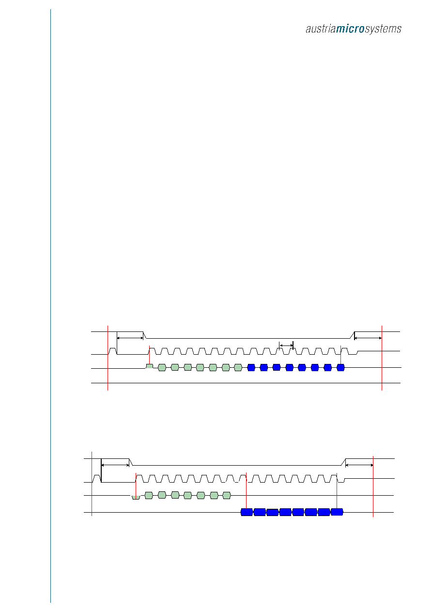
Start up Behavior
Figure 4
Start up and sleep mode behavior of AS8446 (simplified timing)
Vbat
nPORraw
nPOR
VPok
Mcalib
Wake-up
(VDDraw)
(VDD)
(Charge
pump enable)
(calibration
ready)
14 V
4.3 V
5.0 V
100 us ... 500 us
time is user defined by LIN wake up
200 us
Charge pump
start up
m
e
as
u
r
em
e
n
t
un
it
c
a
l
i
b
r
at
io
n
system enable
(normal work)
SPI sends 1 to
R17 (sleep)
sleep mode
300 us
wa
k
e
u
p
t = t1
t
t2
t3
t4
t5
SPI communication possible
300 us
Sleep R17
not
defined
Failure R18
14 V
not defined
5.0 V
not
defined
Registers
R1 to R16
defined
(start-up)
defined by SPI and/or
failure detection units
not defined
wa
ke
u
p
sleep mode
new system
start-up
t = t1 + T
defined by SPI
first system start-up (connection of Vbat to the system)
defined
(start-up)
sleep mode
driver enable
RESET
5.0 V
4.3 V
4.3 V
20 us
possible RESET by watch dog
redefined
(start-up)
RESET by nPOR
RESET by nPOR

Data Sheet AS8446
Revision 1.8, Date 2005-03-17
Page 10 of 35
Programming Capabilities
There are in total 18 registers to program the behavior of the AS8446 via the Three Wire Interface
Register No
Register Name
Meaning
R1<4:0>
SRon
EMC parameter 1, rising edge
R2<4:0>
SRon_stat
EMC parameter 2, rising edge
R3<2:0>
SRon_min
EMC parameter 3, rising edge
R4<4:0>
SRoff
EMC parameter 1, falling edge
R5<3:0>
Sroff_stat
EMC parameter 2, falling edge
R6<1:0>
Acu_on/off
EMC parameter, rising and falling edge, multiplying factor 1 or 2
R7<4:0>
AV_TRIMM
Motor current measurement amplification (steps of 1.25%)
R8<1:0>
AV_RANG_norm
Motor current measurement amplification, normal measurement channel (large
steps)
R9<2:0>
OVERC_level
Over current threshold value
R10<1:0>
AV_RANG_over
Motor current measurement amplification, over current measurement channel
(large steps)
R11<2:0>
VBAT_RANG
Range of supply voltage (max. battery voltage to measure)
R12<2:0>
OVER_VOLT
Over voltage threshold value
R13<2:0>
UNDER_VOLT
Under voltage threshold value
R14<0:0>
VPUMP_MIN
Min. pumped voltage (Vpump ≠ Vbat)
R15<3:0>
ADC_CH
Selection of one of the analog channel to be connected to pin ADC (Analog-
MUX)
R16<0:0>
WATCH_D
Switch on or off of watch dog function
R17<1:0>
SLEEP
Switch on or off of sleep mode
R18<7:0>
FAILURE_STAT
Failure status register
Full descriptions of all registers see below.
Table 10
Meaning of the AS 8446 registers.
Driver Programming (Slew Rate Regulation Parameters)
The Power FET driver is controlled in two different ways:
1. By the digital input PWM (output of the PWM generator of the
µP) to realize the PWM duty cycle of the motor drive for
regulating the motor current, speed or voltage in the closed loop.
2. By the dynamically self-adjusting slew rate regulated switching technology during the rising and falling edges of the
motor voltage.
There are 6 registers to program the driving parameters in different time intervals of the rising and the falling edge of the motor
voltage independently (definition of the time functions of the power FET driver gate currents in wide ranges):
Rising edge: registers R1<4:0>, R2<4:0>, R3<2:0> and R6<0>
Falling edge: registers R4<4:0>, R5<3:0> and R6<1>
These registers can be programmed via the Three-Wire Interface and thus the EMC behavior of the system (motor, power
switches, cables) can be adapted and optimized to a particular application. Although the total rising and falling times are very
short ( t
RISE
or t
FALL
< 150 ns with driver currents to the power FET gate up to 500 mA), the RF emission (EMC) is very low.
See also section Summary of all programmable registers (parameters, functions).
A detailed description of these programming and EMC optimization will be given in the application manual of the AS8446.

Data Sheet AS8446
Revision 1.8, Date 2005-03-17
Page 11 of 35
Rising edge (switch on): Programmable Gate Drive Source Currents (13 bit)
Register / timing
part of rising edge
Programmable range
Programmable range
Unit
Note
R6<0> = 1, Acu_on/off
R6<0> = 0, Acu_on/off
min
max
step
min
max
step
R1<4:0> = SRon
(V
motor
= 12.7 V)
0
496
16
0
248
8
mA
R1<4:0> = SRon
(V
motor
= 30.7 V)
0
(1240)
1
40
0
(620)
1
20
mA
R1 = 0, 1, 2, ... 31
R2<3:0> = SRon_stat
1.0
32
1.0
0.5
16
0.5
mA
R2 = 0, 1, 2, ... 15
R3<2:0> = SRon_min
(V
motor
= -0.5 V)
20
160
20
10
80
10
mA
R3 = 0, 1, 2, ... 7
Note (1):
The total driver current I
out_on
must be limited to 500 mA (I
out_on
< 500 mA ) in the real application with the given
V
motor_max
= V
bat
by appropriate programming.
Table 11
Programming of the slew rate parameters (rising edge)
Figure 5
Rising edge of the motor voltage before and after the EMC optimization

Data Sheet AS8446
Revision 1.8, Date 2005-03-17
Page 12 of 35
Falling edge (switch off): Programmable Gate Drive Sink Currents (10 bit)
Register / timing
part of falling edge
Programmable range
Programmable range
Unit
Note
R6<1> = 1, Acu_on/off
R6<1> = 0, Acu_on/off
min
max
step
min
max
step
R4<4:0> = SRoff
(V
motor
= 12.7 V)
0
496
16
0
248
8
mA
R4<4:0>, SRoff
(V
motor
= 30.7 V)
0
(1240)
1
40
0
(620)
1
20
mA
R4 = 0, 1, 2, ... 31
R5<3:0>, SRoff_stat
1.0
32
1.0
5
80
5
mA
R2 = 0, 1, 2, ... 15
Note (1):
The total driver current I
out_on
must be limited to 500 mA (I
out_on
< 500 mA ) in the real application with the given
V
motor_max
= V
bat
by appropriate programming.
Table 12
Programming of the slew rate parameters (falling edge)
Figure 6
Falling edge of the motor voltage before and after the EMC optimization
-10
0
10
20
30
40
50
60
70
80
0.1
1
10
100
1000
[MHz]
[d
Bµ
V
]
DUT:
Demo board AS8444_TC
Conditions:
V
BAT
= 13.5 V
Load : Ri = 0.4 Ohm, Li = 0.063 mH
EMC parameter set 1 (not EMC optimized)
EMC parameter set 2 (EMC optimized)
I B E E
Ingenieurb¸ro f¸r industrielle Elektrotechnik/ Elektronik
Prof. Dr.-Ing. habil. D. Sperling
Conducted Emission power supply lines according CISPR 25
Detector:
Peak
EMC parameter set 1
(not EMC optimized)
EMC parameter set 2
(EMC optimized)
Figure 7
Comparison of the EMC measurement results of the same application with two different EMC parameter sets

Data Sheet AS8446
Revision 1.8, Date 2005-03-17
Page 13 of 35
Programming of the motor current measurement unit and the over current detection unit
The motor current measurement unit operates with an external current measurement resistor R
meas
in the high side motor line.
The chip has two measurement amplification channels with separately programmable amplification factors:
a)
normal motor current measurement, channel 1
AV
meas_norm
= V
A_current
/ V
meas
with V
meas
= (V
CMP
- V
CMN
), analog output A_current (multiplexed to output ADC) and
b)
over current measurement with extended measurement range, channel 2
AV
meas_overc
= V
A_overc
/ V
meas
, analog output A_overc (multiplexed to output ADC).
In general all programming possibilities in table 14 can be used to build up a measurement system in the defined limits. The
programming words are sent from the
µP via the Three-Wire Interface to the AS8446 during start up of the system. The typical
value of V
meas_nom
= (V
CMP
- V
CMN
)
nom
is 50 mV, corresponding to 100% of the motor current.
In the whole system the analog outputs A_current or A_overc are used by the ADC of the
µP to regulate and control the
system. There is only one exception: The over current detection and protection is realized directly by the over current
measurement channel in order to act very fast in case of an over current situation e.g. short circuit of the motor.
Figure 8 Programming examples of the current
Figure 9 Programming examples of the over current
measurement channels
detection
Figure 8 shows the programming of the normal current measurement channel (red lines, output voltage VCUR) and the over
current measurement channel with extended measurement range (blue lines, output voltage VCOVER). The three lines with the
parameters AV_TRIMM = 70, 80, 90 indicate the trimming range of the external measurement resistor (+ 12.5 % in steps of 1.25
%). The total range of the normal measurement amplification is AV
meas_norm
= 70 to 360 corresponding to input voltages
V
meas_max
= 11 mV to 57 mV. The total range of the over current measurement amplification is AV
meas_overc
= 17.5 to 90
corresponding to input voltages V
meas_max
= 44 mV to 229 mV.
Figure 9 shows an example of the programming of the over current threshold level (generation of the over current signal VPOV,
red lines): AV
meas_overc
= 20 and OVERC_level = 0.5 V to 4.0 V in steps of 0.5 V.
All programming possibilities are given in table 14 below.

Data Sheet AS8446
Revision 1.8, Date 2005-03-17
Page 14 of 35
Programming of the motor current measurement and over current detection unit
The motor current measurement unit transforms the differential voltage over the measurement resistor at the high side
motor line (V
CMP
- V
CMN
) = Imotor * Rmeas to the ground related voltage V
A_current
(channel1) and to the ground related
voltage V
A_overc
(channel2) with a programmable amplification.
Definition and programming of the voltage amplifications AV
meas_norm
and AV
meas_overc
of the motor current measurement
unit:
a) channel 1: AV
meas_norm
= V
A_current
/ (V
CMP
- V
CMN
) = AV_TRIMM * AV_RANGE_norm
b) channel 2: AV
meas_overc
= V
A_overc
/ (V
CMP
- V
CMN
) = AV_TRIMM * AV_RANGE_over
Register No
Register Name
Meaning
R7<4:0>
AV_TRIMM
Voltage amplification factor1 of the current measurement unit in
small steps (trimming of the external current measurement resistor)
for the normal and over current analog measurement output
R7 = 0
ý AV_TRIMM = 70
R7 = 1
ý AV_TRIMM = 71
R7 = 2
ý AV_TRIMM = 72
:
R7 = 10
ý AV_TRIMM = 80
(default value)
R7 = 11
ý AV_TRIMM = 81
:
R7 = 19
ý AV_TRIMM = 89
R7 = 20
ý AV_TRIMM = 90
R7 > 20
ý AV_TRIMM = 90
R8<1:0>
AV_RANGE
Voltage amplification factor2 of the normal analog measurement
output (A_current)
R8 = 0
ý AV_RANGE = 1
(default value)
R8 = 1
ý AV_RANGE = 2
R8 = 2
ý AV_RANGE = 3
R8 = 3
ý AV_RANGE = 4
R9<2:0>
OVERC_level
Threshold value of the internal over current detection
Def.: Vocmax = 4/5 * VDD
(typ. 4.0 V)
Vocstep = (4/5 * VDD) / 8
(typ. 0.5 V)
R9 = 0
ý OVERC_level = Vocmax
(typ. 4.0 V)
R9 = 1
ý OVERC_level = Vocmax ≠ Vocstep
(typ. 3.5 V)
R9 = 2
ý OVERC_level = Vocmax - 2*Vocstep
(typ. 3.0 V)
R9 = 3
ý OVERC_level = Vocmax - 3*Vocstep
(typ. 2.5 V)
:
R9 = 7
ý OVERC_level = Vocmax - 7*Vocstep
(typ. 0.5 V)
R10<1:0>
AV_RANGE_over
Voltage amplification factor2 of the over current analog
measurement output (A_overc)
R10 = 0
ý AV_RANGE_over = 1 * 1/4 (default value)
R10 = 1
ý AV_RANGE_over = 2 * 1/4
R10 = 2
ý AV_RANGE_over = 3 * 1/4
R10 = 3
ý AV_RANGE_over = 4 * 1/4
Remark 1: The maximum of the valid analog output voltage of the outputs A_current and A_overc must be 4.0 V.
Remark 2: The total voltage amplification of the current measurement unit is determined by
normal current analog output A_current: AV
meas_norm
= V
A_current
/ (V
CMP
- V
CMN
) = AV_TRIMM * AV_RANGE
(default value: 80)
over current analog output A_overc: AV
meas_overc
= V
A_overc
/ (V
CMP
- V
CMN
) = AV_TRIMM * AV_RANGE_over
(default value: 20)

Data Sheet AS8446
Revision 1.8, Date 2005-03-17
Page 15 of 35
Remark 3: The external current measurement voltage over the measurement resistor Rmeas
(V
CMP
- V
CMN
) = Imotor * Rmeas where the internal over current detection is switched on can be
determined by: (V
CMP
- V
CMN
)
overc
* AV_TRIMM * AV_RANGE_over = OVERC_level
(V
CMP
- V
CMN
)
overc
= OVERC_level / (AV_TRIMM * AV_RANGE_over)
example: OVERC_level = 4 V, AV_TRIMM = 80, AV_RANGE_over = 1/4
ý (V
CMP
- V
CMN
)
overc
= 200 mV
Remark 4: Example of the programming of the current measurement / over current detection unit:
Step1: Definition of the nominal voltage drop over the external current measurement resistor Rmeas
(V
CMP
- V
CMN
)
nom
= Imotor
nom
* Rmeas e.g. (V
CMP
- V
CMN
)
nom
= 50 A * 1 m
= 50 mV
Step2: Definition of the over current threshold value of (V
CMP
- V
CMN
) e.g. (V
CMP
- V
CMN
)
overc
= 100 mV
Step3: Determination of the voltage amplification of the normal current measurement channel so that the nominal
output voltage V
A_current_nom
= 4.0 V
e.g. AV_TRIMM * AV_RANGE = 80 * 1
ý V
A_current-nom
= 50 mV * 80 = 4.0 V
Step4: Determination of the voltage amplification of the over current measurement
e.g. AV_TRIMM * AV_RANGE_over = 80 * 1/4
ý V
A_overc_max
= 100mV * 20 = 2.0 V < 4.0 V
Step5: Determination of the programming of the internal over current threshold value (OVERC_level)
With the formula: (V
CMP
- V
CMN
)
overc
= OVERC_level / (AV_TRIMM * AV_RANGE_over) and all values
above:
OVERC_level = (V
CMP
- V
CMN
)
overc
* (AV_TRIMM * AV_RANGE_over) = 100 mV * 80 *1/4 = 2.0 V
ý R9 = 4
Remark 5: The amplifications AV
meas_norm
and AV
meas_overc
of the current measurement unit can be adapted to the
external measurement resistor R
meas
by the programming word AV_TRIMM in steps of 1.25 % in the range
of + 12.5% (trimming of R
meas
).
Table 13
Programming of the motor current measurement an over current detection unit

Data Sheet AS8446
Revision 1.8, Date 2005-03-17
Page 16 of 35
Summary of all programmable registers (parameters, functions)
Register /
address
Internal name
Meaning
Note
Ra<b1:b0> means: address = a, most significant data bit = b1, least significant data bit = b0
All registers can be write and read by the Three-Wire Interface (write priority has the Three-Wire Interface).
1. The start up reset of all registers unless the R17 and the R18 is done by the signal nPOR (controlled by the VDD).
2. The start up reset of the register R17 is done by the nPORraw (controlled by the voltage VDDraw) only.
3. The start up reset of the register R18 (failure register) is done with a delay after the nPOR, this delay is generated
by the enable signal of the charge pump VPok.
Programming of the driver output currents (independent for switch on and switch off)
R0<7:0>
Not used
Slew rate regulation programming, on switch,
voltage V
Vmo
dependent driver output current for positive V
VMO
voltage
SRon = 0, 1, 2, ... 31
I
SRon
= V
Vmo
* Acu_on * SRon * K1 V
VMO
> 0
Register write by: Three Wire Interface
Register read by: Three Wire Interface and FET driver unit
-
-
-
d4
d3
d2
d1
d0
R1<4:0>
SRon
-
-
-
1
1
1
1
1
start up values
Slew rate regulation programming, on switch,
constant driver output current
SRon_stat = 0, 1, 2, ... 31
I
SRon_stat
= 2.0
µA * (SRon_stat + 1) * Acu_on
Register write by: Three Wire Interface
Register read by: Three Wire Interface and FET driver unit
-
-
-
d4
d3
d2
d1
d0
R2<4:0>
SRon_stat
-
-
-
1
1
1
1
1
start up values
Slew rate regulation programming, on switch,
voltage V
VMO
dependent driver output current for negative V
VMO
voltage
SRon_min = 0, 1, 2, ...7
I
SRon_min
= V
Vmo
* (SRon_min + 1) *Acu_on * K2 V
VMO
< 0
Register write by: Three Wire Interface
Register read by: Three Wire Interface and FET driver unit
-
-
-
-
-
d2
d1
d0
R3<2:0>
SRon_min
-
-
-
-
-
1
1
1
start up values

Data Sheet AS8446
Revision 1.8, Date 2005-03-17
Page 17 of 35
Slew rate regulation programming, off switch,
voltage V
VMO
dependent driver input current for positive V
VMO
voltage
SRoff = 0, 1, 2, ... 31
I
SRoff
= V
Vmo
* Acu_off * SRoff * K3
Register write by: Three Wire Interface
Register read by: Three Wire Interface and FET driver unit
-
-
-
d4
d3
d2
d1
d0
R4<4:0>
SRoff
-
-
-
1
1
1
1
1
start up values
Slew rate regulation programming, off switch,
constant driver input current
SRoff_stat = 0, 1, 2, ... 15
I
SRoff_stat
= 20
µA * (SRoff_stat + 1) * Acu_off
Register write by: Three Wire Interface
Register read by: Three Wire Interface and FET driver unit
-
-
-
-
d3
d2
d1
d0
R5<3:0>
SRoff_stat
-
-
-
-
1
1
1
1
start up values
Current amplification of the driver for on and off switch
R6<0> = 0
ý Acu_on = (Iout / Iin)
on
= 256
R6<0> = 1
ý Acu_on = (Iout / Iin)
on
= 512
R6<1> = 0
ý Acu_off = (Iout / Iin)
off
= 256
R6<1> = 1
ý Acu_off = (Iout / Iin)
off
= 512
Register write by: Three Wire Interface
Register read by: Three Wire Interface and FET driver unit
-
-
-
-
-
-
Acu_off
Acu_on
R6<1:0>
Acu_on Acu_off
-
-
-
-
-
-
0
0
start up values
Programming of the motor current measurement and over current detection unit
The motor current measurement unit transforms the differential voltage over the measurement resistor
(V
CMP
- V
CMN
) = Imotor * Rmeas to the ground related voltages V
A_current
(channel1: normal current measurement channel) and
V
A_overc
(channel2: over current measurement channel) with a programmable amplification.
Def. of the voltage amplification of the motor current measurement unit:
Voltage amplification of the normal current measurement channel:
1.
AV
meas_norm
= V
A_current
/ (V
CMP
- V
CMN
) = AV_TRIMM * AV_RANGE_norm
Voltage amplification of the normal current measurement channel
2.
AV
meas_overc
= V
A_overc
/ (V
CMP
- V
CMN
) = AV_TRIMM * AV_RANGE_over

Data Sheet AS8446
Revision 1.8, Date 2005-03-17
Page 18 of 35
R7 = 0
ý AV_TRIMM = 70
R7 = 1
ý AV_TRIMM = 71
R7 = 2
ý AV_TRIMM = 72
:
R7 = 10
ý AV_TRIMM = 80 (default value)
R7 = 11
ý AV_TRIMM = 81
:
R7 = 19
ý AV_TRIMM = 89
R7 = 20
ý AV_TRIMM = 90
R7 > 20
ý AV_TRIMM = 90
Register write by: Three-Wire Interface
Register read by: Three-Wire Interface and current measurement unit
-
-
-
d4
d3
d2
d1
d0
R7<4:0>
AV_TRIMM
-
-
-
0
1
0
1
0
start up values
R8 = 0
ý AV_RANGE-norm = 1 (default value)
R8 = 1
ý AV_RANGE-norm = 2
R8 = 2
ý AV_RANGE-norm = 3
R8 = 3
ý AV_RANGE-norm = 4
Register write by: Three-Wire Interface
Register read by: Three-Wire Interface and current measurement unit
-
-
-
-
-
-
d1
d0
R8<1:0>
AV_RANGE_norm
-
-
-
-
-
-
0
0
start up values
Threshold value of the internal over current detection
Def.: Vocmax = 4/5 * VDD
(typ. 4.0 V)
Vocstep = (4/5 * VDD) / 8
(typ. 0.5 V)
R9 = 0
ý OVERC_level = Vocmax
(typ. 4.0 V)
R9 = 1
ý OVERC_level = Vocmax ≠ Vocstep
(typ. 3.5 V)
R9 = 2
ý OVERC_level = Vocmax - 2*Vocstep
(typ. 3.0 V)
R9 = 3
ý OVERC_level = Vocmax - 3*Vocstep
(typ. 2.5 V)
:
R9 = 7
ý OVERC_level = Vocmax - 7*Vocstep
(typ. 0.5 V)
Register write by: Three-Wire Interface
Register read by: Three-Wire Interface and current measurement unit
-
-
-
-
-
d2
d1
d0
R9<2:0>
OVERC_level
-
-
-
-
-
0
1
1
start up values
Voltage amplification factor2 of the over current analogue measurement
output (A_overc)
R10 = 0
ý AV_RANGE_over = 1 * 1/4 (default value)
R10 = 1
ý AV_RANGE_over = 2 * 1/4
R10 = 2
ý AV_RANGE_over = 3 * 1/4
R10 = 3
ý AV_RANGE_over = 4 * 1/4
Register write by: Three-Wire Interface
Register read by: Three-Wire Interface and current measurement unit
-
-
-
-
-
-
d1
d0
R10<1:0>
AV_RANGE_over
-
-
-
-
-
-
0
0
start up values

Data Sheet AS8446
Revision 1.8, Date 2005-03-17
Page 19 of 35
Programming of the battery voltage monitor and over / under voltage detection
R11= 0
ý VBAT_RANGE = 5 ý Vbat-max = 20 V
R11= 1
ý VBAT_RANGE = 8 ý Vbat-max = 32 V
R11= 2
ý VBAT_RANGE = 10 ý Vbat-max = 40 V
R11= 3
ý VBAT_RANGE = 15 ý Vbat-max = 60 V
R11= 4
ý VBAT_RANGE = 20 ý Vbat-max = 80 V
Register write by: Three-Wire Interface
Register read by: Three-Wire Interface and voltage monitor
-
-
-
-
-
d2
d1
d0
R11<2:0>
VBAT_RANGE
-
-
-
-
-
0
1
0
start up values
R11= 0
ý VBAT_RANGE = 5 ý Vbat-max = 20 V
R11= 1
ý VBAT_RANGE = 8 ý Vbat-max = 32 V
R11= 2
ý VBAT_RANGE = 10 ý Vbat-max = 40 V
R11= 3
ý VBAT_RANGE = 15 ý Vbat-max = 60 V
R11= 4
ý VBAT_RANGE = 20 ý Vbat-max = 80 V
Register write by: Three-Wire Interface
Register read by: Three-Wire Interface and voltage monitor
-
-
-
-
-
d2
d1
d0
R12<2:0>
OVER_VOLT
-
-
-
-
-
1
1
1
start up values
Step of UNDER_VOLT = 0.25 V * VBAT_RANGE
UNDER_VOLT = 0.25 V * VBAT_RANGE * (R13 + 1)
Start up value: UNDER_VOLT = 7.5 V
Register write by: Three-Wire Interface
Register read by: Three-Wire Interface and voltage monitor
-
-
-
-
-
d2
d1
d0
R13<2:0>
UNDER_VOLT
-
-
-
-
-
0
0
0
start up values
Programming of the charge pump voltages
R14 = 0
ý VPUMP_MIN = 4.0 V
R14 = 1
ý VPUMP_MIN = 6.0 V
Register write by: Three-Wire Interface
Register read by: Three-Wire Interface and charge pump
-
-
-
-
-
-
-
d0
R14<0:0>
VPUMP_MIN
-
-
-
-
-
-
-
0
start up values

Data Sheet AS8446
Revision 1.8, Date 2005-03-17
Page 20 of 35
Programming of the analog MUX
R15 = 0
ý A_current
(normal current measurement channel)
R15 = 1
ý A_overc
(over current measurement channel)
R15 = 2
ý Vbat_mon
(Vbat measurement channel)
R15 = 3
ý TP
(temperature measurement channel)
The following signals can be given at the ADC output for chip test
purposes:
R15 = 4
ý Vtemp
(temperature voltage of the internal sensor)
R15 = 5
ý PVover
(Over voltage Vbat signal)
R15 = 6
ý PVunder
(Under voltage Vbat signal)
R15 = 7
ý PTover_in
(Over temperature signal, internal)
R15 = 8
ý PTover_ex
(Over temperature signal, external)
Register write by: Three-Wire Interface
Register read by: Three-Wire Interface and analog MUX
-
-
-
-
d3
d2
d1
d0
R15<3:0>
ADC_CH
-
-
-
-
0
0
0
0
start up values
Note:
Do not switch the analog MUX during operation!
Programming of the watch dog
R16 = 0
ý watch dog is off (watch dog not used)
R16 =1
ý watch dog is on (watch dog used)
Register write by: Three-Wire Interface
Register read by: Three-Wire Interface and watch dog
-
-
-
-
-
-
-
d0
R16<0:0>
WATCH_D
-
-
-
-
-
-
-
0
start up values
Programming of the sleep mode
R17 = 0
ý no sleep mode (normal operation)
R17 = 1
ý sleep mode (power down)
Register reset to low by the Wake-up Interface.
Wake-up = low (high / low edge)
ý R17<0:0> set to low
-
-
-
-
-
-
-
d0
R17<0:0>
SLEEP
-
-
-
-
-
-
-
1
start up values

Data Sheet AS8446
Revision 1.8, Date 2005-03-17
Page 21 of 35
Failure Registers and Test Mode Register (on chip temperature detection)
R18<7:0>
FAILURE_STAT
R18<0>
ý Poverc
(bit 0 contains the over current status)
R18<1>
ý PVover
(bit 1 contains the over voltage status of Vbat)
R18<2>
ý PVunder
(bit 2 contains the under voltage status of Vbat)
R18<3>
ý PTover_in
(bit 3 contains the on chip over temperature status)
R18<4>
ý PTover_ex
(bit 4 contains the external over temperature status)
R18<5>
ý VDDover
(bit 5 contains the over voltage status of VDD, 5 V)
R18<6>
ý VDDunder
(bit 6 contains the under voltage status of VDD, 5 V)
R18<7> = 0
ý
band gap Voltage is the reference voltage for the
on chip over temperature detection (normal function)
R18<7> = 1
ý
the voltage at pin TP is the reference voltage for
the on chip over temperature detection (test mode)
Registers R18<6:0>
set and reset by Three-Wire Interface and only
set by corresponding failure detection units
(Three Wire-Interface has write priority)
Register R18<6:0>
read by Three-Wire Interface and corresponding
logic
Register R18<7>
write by Three-Wire Interface only
Register R18<7>
read by Three-Wire Interface and corresponding
analog switch
TEMP_TEST
VDDunder
VDDover
PTover_ex
PTover_in
PVunder
PVover
Poverc
0
0
0
0
0
0
0
0
start up values
Table 14
Summary of the programming capabilities of the AS 8446
Data Sheet AS8446
Revision 1.8, Date 2005-03-17
Page 22 of 35
Three -Wire
µP-Interface
Data transfer from the microprocessor or PC to the AS8446 and vice versa is accomplished by means of Three-Wire Interface.
The Three-Wire Interface of the AS8446 acts generally in slave mode. The master in the whole regulator board is either the
controlling
µP (normal regulator module in volume production) or a PC (development or field programming mode e.g. to realize
the EMC optimization).
All registers (see section Summary of all programmable registers (parameters, functions)) can be written and read by the
Three-Wire Interface.
Pin DATAout is high ohmic if the Three-Wire Interface chip select signal CS is not active (high).
During an over voltage situation the write access to the Three-Wire Interface is blocked.
Physical Interface
Supported modes, and bit order are shown in Figure 10 and Figure 11.
The DATAin signal must be valid with the rising edge of the clock Clk, the DATAout is valid with the falling edge of
the clock Clk.
The clock frequency should be as low as useful in the particular application. It is recommended not to use a clock
frequency f
clk
higher than 10 MHz.
The MSB is always transmitted / received first.
LSB
CS
Clk
DATAin
DATAout
HEADER
DATA
MSB
> 30 us
first frame
next
frame
LSB
MSB
> 0.1 us
> 30 us
Figure 10
Physical Interface of Three-Wire Interface in write mode
LSB
CS
Clk
DATAin
DATAout
HEADER
DATA
MSB
LSB
> 30 us
first frame
next
frame
MSB
> 30 us
Figure 11
Physical Interface of Three-Wire Interface in read mode

Data Sheet AS8446
Revision 1.8, Date 2005-03-17
Page 23 of 35
Communication Protocol
The Three-Wire Interface -interface acts as communication interface between the µP or PC and the registers within the AS8446.
For efficient register access, a protocol has been defined with the following features:
Purely master-slave protocol with µP or PC as master
Two different frames: One read and one write frame
Frame is delimited by the status of CS (CS = frame delimiter or chip select signal), one frame consists of 16 Bits (header byte
and data byte).
Special remark for interface lock condition: If a frame does not consist of 16 bits (can be caused e.g. by spiking, noise or
interrupt), the interface will be locked. In order to leave this lock situation CS = high and one or several clock pulses must be
set. Setting CS = high alone will not be sufficient.
Referring to Figure 10 and Figure 11, a Clk pulse with CS = high must be set in order to reset the interface and to ensure a safe
communication.
Data Fields
HEADER H
MSB
H
LSB
R/W
-
-
A4
A3
A2
A1
A0
A4, A3, A2, A1, A0: Address A (Register address to read or to write)
R/W = MSB, A0 = LSB.
R/W: Read or Write
R/W =0: Read (Data are read/transmitted from the AS8446 via the DATAout pin.)
R/W =1: Write (Data are write/transmitted from the µP or PC to the AS8446 via the DATAin pin.)
DATA D
MSB
D
LSB
D7
D6
D5
D4
D3
D2
D1
D0
D7...D0: Data (Denotes the data of the register addressed. D7=MSB, D0=LSB)
Note:
To ensure a correct register setting the use of µP based verification (Write, Read-Back, Verify) is mandatory.

Data Sheet AS8446
Revision 1.8, Date 2005-03-17
Page 24 of 35
Electrical Parameters and Functionality of the Subblocks
All parameters are valid in the temperature range Tamb = -40
o
C to +125
o
C if not otherwise mentioned.
5V Regulator
PARAMETER
SYMBOL
MIN
TYP
MAX
UNIT
NOTE
Regulated Output Voltage
VDD
4.8
5.0
5.15
V
(1)
Load Current at VDD
IOUT
40
mA
(2), (3), (4)
Under voltage detection threshold
VDDunder
4.3
V
Over voltage detection threshold
VDDover
5.6
V
Note (1): For use of the internal voltage regulator the Pins V
DD
and V
DDctrl
must be connected. An external
capacitor of 4.7
µF to 10µF needs to be connected at the VDD pin.
Note (2): Valid for Vbat
6.5V; for 6.0V Vbat < 6.5V the load current is limited to 2.5mA.
Note (3): There is also the possibility to use an external regulator (Bipolar transistor). It is up to the user to select
the suitable external components.
Note (4): The max. power dissipation on chip must be respected
(estimation: Pchip_vdd = ((Vbatmax - 5 V ) * Ivdd_ex + Vbat * Ivdd_in) < 400 mW )
Design Example
Figure 12: Design example for operation of external voltage regulator
Power on Reset
2
1
3
4
5
0
2
1
3
4
5
5
4
3
2
1
Figure 13
Transfer characteristic of PORn circuitry
T
1
... Philips NPN medium power transistor BCX 56
C
VDD
... Panasonic FK-series 100µF / 16V
R
100
C
VDD
100 µF / 16V
T
1
V
BAT
220 nF
(Ceramic)
V
DDctrl
V
DD
47 nF

Data Sheet AS8446
Revision 1.8, Date 2005-03-17
Page 25 of 35
PARAMETER
SYMBOL
MIN
TYP
MAX
UNIT
NOTE
Off threshold for Reset generation
Voff_PORS
2.1
3.5
4.5
V
Ramp up
Hysteresis of Reset signal
Hyst_PORS
0.1
0.8
V
Sleep / wake up system
The whole IC is put in sleep mode (power down mode) by the control signal SLEEP set via the Three Wire Interface (SLEEP =
high, content register R17).
The whole start up and sleep mode behavior is shown in figure 4.
In sleep mode the following actions are done:
-
the power FET driver output OUT is hold at low (VSS)
-
the oscillator, the charge pump and all other blocks are put in a high ohmic status
-
the 5 V regulator is switched off (no external supply at pin VDD, this way all devices on the motor regulator board supplied
by VDD, e.g. the
µP and the external temperature sensor, are powered down)
-
a raw internal 5 V supply V
DDraw
is generated to supply the wake up system and the whole logic block
-
the total current consumption of the IC is less than 90
µA
During sleep mode the Wake-up Pin must be at high level (V
BAT
).
Applying a "low"-pulse on the wake-up pin will wake up the IC.
PARAMETER
SYMBOL
MIN
TYP
MAX
UNIT
NOTE
Current Consumption in Sleep Mode
(Tamb = -40
o
C to 125
o
C)
Ivbat_pd
90
µA
Current Consumption in Sleep Mode
(Tamb = -40
o
C to 27
o
C) (1)
Ivbat_pd27
(50)
µA
R17<0> = 1 (SLEEP =
high)
Note (1): only as information. Will not be tested.
Reference Current Generator
The reference current generator uses a bandgap based 1 V reference voltage to generate a buffered 1 V voltage reference at
pin Iref. A 22 k
external resistor must be used to generate the 45 µA current reference.
PARAMETER
SYMBOL
MIN
TYP
MAX
UNIT
NOTE
Voltage at pin Iref
Vref
0.95
1.0
1.05
V
High Side Power FET Driver / Slew Rate Regulation
The supply voltage of this driver is about 10 V higher than the Vbat (n-channel power FET to drive) and is delivered by the on
chip charge pump at pin Vpump.
The Power FET driver is controlled in two different ways:
First by the digital output of the PWM generator of the
µP to realizing a certain duty cycle of the motor drive and so to regulate
the motor current, voltage or speed in a closed loop.
The driver output OUT is set to low (the motor is switched off) independently of the PWM signal under the following conditions:
∑
over current condition:
The over current signal Poverc is set to high by the over
(Poverc = high
)
current detection unit and reset to low via the Three Wire Interface
∑
under voltage condition of Vbat:
The under voltage signal PVunder is set and reset by the voltage
(PVunder = high)
monitor.
∑
over voltage condition of Vbat:
The over voltage signal PVover is set and reset by the voltage
(PVover = high )
monitor.

Data Sheet AS8446
Revision 1.8, Date 2005-03-17
Page 26 of 35
∑
charge pump voltage Vpump - Vbat is too low:
The charge pump OK signal VPok is set and reset by the charge pump
(VPok = low )
monitor.
The threshold values of these parameters are programmable (see section Summary of all programmable registers
(parameters, functions)).
∑
the calibration of the motor current measurement unit is not yet finished: Mcalib = low. The motor current must be zero
respectively the voltage (V
CMP
- V
CMN
) must be zero during the calibration.
This calibration is done after the start up of the system including the ready signal of the charge pump: power on reset signal
nPOR and Vpok = high starts the calibration. The calibration procedure needs about 200
µs (see figure 4).
Summary of logic driver function: OUT = PWM and /Poverc and /PVunder and /PVover and VPok and Mcalib
Second by the analog motor voltage to regulate the slew rate during the rising and falling edge of the motor voltage (EMC
conform technology). This slew rate control respectively regulation is executed by a feedback of the motor voltage V
motor
available at the pin Vmo. The characteristics (parameters) of this slew rate regulation can be programmed via the Three-Wire
Interface independently for the falling and rising edge of the motor voltage and can therefore be adapted to a specific
application (motor and its environment).
This programming of the output current characteristics (gate current of the external power FET) in both directions is shown in
section Summary of all programmable registers (parameters, functions).
PARAMETER
SYMBOL
MIN
TYP
MAX
UNIT
NOTE
Tolerances of driver
output current (pin
OUT), sourcing
IOUTon
-50%
+50%
I
out_on
= I
SRon-stat
+ I
SRon
+ I
SRon_min
The relative tolerances between adjacent
programming steps of the driver current are less
than 10%.
Tolerances of driver
output current (pin
OUT), sinking
IOUToff
-50%
+50%
I
out_off
= I
SRoff-stat
+ I
SRoff
The relative tolerances between adjacent
programming steps of the driver current are less
than 10%.
-
max. pulse duration = 1
µs @ 20 kHz or max. external charge to load: 250 nC @ 20 kHz
-
valid for I
OUT
= 5 mA ... 500 mA and Vbat = 12 V , Vpump = 22 V
-
Programmable by the registers R1 to R6

Data Sheet AS8446
Revision 1.8, Date 2005-03-17
Page 27 of 35
Charge Pump and internal Oscillator
The charge pump is a one-stage pump that generates a pumped voltage Vpump about 10 V higher than the supply voltage Vbat
for Vbat > 13.5 V. It uses two external capacitors only, the capacitor Cp12 as the switched capacitor and Cp0 as the storage
capacitor.
The pumped voltage (Vpump - Vbat) is monitored to detect over or under voltages (protection of the power FET gate):
(Vpump - Vbat) = 10 V to 12 V : Normal voltage regulation of the charge pump
(Vpump - Vbat) < (Vpump - Vbat)
low
: The digital signal VPok is indicating this under voltage and disabling the power FET driver.
The threshold value (Vpump - Vbat)
low
can be programmed to be 6 V or 4 V (VPUMP_MIN).
PARAMETER
SYMBOL
MIN
TYP
MAX
UNIT
NOTE
Pumped voltage
Vpump - Vbat
10
10.5
12
V
Vbat = 13.5 V, Iload = 5 mA
Pumped voltage
Vpump - Vbat
4.0
5.0
V
Vbat = 6.5 V, Iload = 2.5 mA
Pumped voltage
Vpump - Vbat
4.0
V
6.0V
Vbat < 6.5V (low-Battery-
mode), Iload = 250µA
Under voltage threshold
(VPUMP_MIN = 1)
(Vpump - Vbat)
low
5.4
6.0
6.6
V
falling (Vpok)
Under voltage threshold
(VPUMP_MIN = 0)
(Vpump - Vbat)
low
3.4
4.0
4.6
V
falling (Vpok)
regulated voltage
threshold
(Vpump - Vbat)
high
10
10.5
12
V
rising
frequency
f
pump
40
50
70
kHz
Motor Current Measurement Unit / Over Current Detection
The motor current measurement unit functions with an external current measurement resistor R
meas
in the
high side motor line. The chip has two measurement amplification channels with separately programmable amplification factors
AV
meas_normal
= V
A_current
/ (V
CMp
≠ V
CMn
) (analogue output A_current) and AV
meas_over
= V
A_overc
/ (V
CMp
≠ V
CMn
) (analogue output
A_overc). The maximal valid nominal analogue output voltage level V
A_current
and V
A_overc
of theses channels is 4.0 V (100%
value of the output voltage V
A_current
(nominal value).
In general, all programming possibilities can be used to build up a measurement system within the defined limits.
It is recommended to use a nominal differential voltage (V
CMp
≠ V
CMn
) > 50 mV to avoid larger tolerances of the amplification
factor caused by offset.
The programming of theses two amplification channels is usually realized in a way that the measurement range of the over
current measurement channel is wider than the normal current measurement channel.
In the whole system the analogue outputs A_current and A_overc are used via an ADC in the controlling
µP to regulate and
control the system. There is one exception only: The over current detection and protection is realized directly by the over
current measurement channel to be able to act very fast in case of an over current situation (short circuit).
The measurement unit contains a low pass filter to prevent wrong measurement if short transients of the measurement input
voltage occurs (cut-off frequency about 500 kHz).
The motor current measurement unit is endowed with an auto calibration procedure for the offset voltage. The motor current
respectively the measurement voltage (Vcmp - Vcmn) must be zero during this calibration.
This calibration is done after the start up of the system including the ready signal of the charge pump: power on reset signal
nPOR and Vpok = high starts the calibration. The calibration procedure needs about 200
µs.

Data Sheet AS8446
Revision 1.8, Date 2005-03-17
Page 28 of 35
a) Motor current measurement (normal current amplification channel: A
CMV_normal
, programmed by AV_RANGE_norm (Register
R8<1:0>) and AV_TRIMM (Register R7<4:0>)
The nominal measurement differential voltage V
meas_nom
(corresponding to 100% of the nominal motor current)
V
meas_nom
= (V
CMp
≠ V
CMn
)
nom
= I
motor_nom
* R
meas
must be fixed by the value of R
meas
. So the value of this measurement resistor is
given by R
meas
= (V
CMp
≠ V
CMn
)
nom
/ I
motor_nom
.
The voltage amplification of this motor current measurement unit AV
meas_normal
= V
A_current
/ (V
CMp
≠ V
CMn
) is programmable in the
range AV_RANGE_norm * AV_TRIMM = (1, 2, 3, 4) * (70, 71, ... 89, 90)
Examples:
AV_RANGE_norm = 1:
A
CMV_normal
= 70, 71, 72, ... , 80, ... , 89, 90
AV_RANGE_norm = 4:
A
CMV_normal
= 280, 284, 288, ..., 320, ... , 360
(The programming values of AV_RANGE_norm >1 are intended for a measurement of low currents with a higher digital
resolution, but in this cases the tolerances of the amplification factor is high due to the remaining offset of the measurement
amplifier.)
This way the analog output value V
A_current
of the current measurement unit can be adapted to the external measurement resistor
R
meas
(trimming of this resistor in the range + 12.5%).
The nominal (respectively 100%) voltage of the measurement unit V
A_current
(this is the nominal input voltage of the ADC on the
µP) must be 4.0 V.
b) Over current detection and protection (over current amplification channel A
CMV_over
)
The over current amplification channel uses the same input voltage V
meas
= (V
CMp
≠ V
CMn
) as the normal current amplification
channel.
The voltage amplification of this over current measurement channel A
CMV_over
= V
A_overc
/ (V
CMp
≠ V
CMn
) is programmable by
AV_RANGE_over (Register R10<1:0>) and AV_TRIMM (Register R7<4:0>)
in the range
A
CMV_over
= AV_RANGE_over * AV_TRIMM = (1/4, 2/4, 3/4, 4/4) * (70, 71, ... 89, 90)

Data Sheet AS8446
Revision 1.8, Date 2005-03-17
Page 29 of 35
Examples:
AV_RANGE_over = 1/4:
A
CMV_over
= 17.5, 17.75, 18, ... , 20, ... , 22.25 , 22.5
AV_RANGE_over = 4/4:
A
CMV_over
= 70, 71, 72, ..., 80, ... , 89, 90
The adjustment (trimming) of the measurement resistor R
meas
is realized by the same programming parameter AV_TRIMM (+
12.5%) like in a).
The maximal output voltage of the over current amplification channel V
A_overc
(this is the nominal input voltage of the ADC on the
µP) must be 4.0 V.
The threshold value of the over current detection can be programmed by the programming parameters OVERC_level (in
conjunction with AV_RANGE_over and AV_TRIMM) in the following way.
The voltage over the external measurement resistor where the over current situation is detected (Vmeas_over) is given by:
V
meas_over
= OVERC_level / (AV_TRIMM * AV_RANGE_over) with
OVERC_level = 0.5 V, 1.0 V, 1.5 V, ... 4.0 V
See also section Summary of all programmable registers (parameters, functions) for the programming of the parameters
above.
PARAMETER
SYMBOL
MIN
MAX
UNIT
NOTE (Programming, nominal amplification)
- 6
+ 6
%
V
meas
= 50 mV, R8 = 0
ý 80
- 10
+ 10
%
V
meas
= 25 mV, R8 = 1
ý 160
- 20
+ 20
%
V
meas
= 16.67mV, R8 = 2
ý 240
Tolerance of voltage
amplification, normal
current measurement
channel
1)
A
CMV_normal
- 20
+ 20
%
V
meas
= 12.5 mV, R8 = 3
ý 360
- 6
+ 6
%
V
meas
= 200 mV, R10 = 0
ý 20
- 6
+ 6
%
V
meas
= 100 mV, R10 = 1
ý 40
- 6
+ 6
%
V
meas
= 60.6 mV, R10 = 2
ý 60
Tolerance of voltage
amplification, over
current measurement
channel
1)
A
CMV_over
- 6
+ 6
%
V
meas
= 50 mV, R10 = 3
ý 80
Tolerance of linearity
A
CMV_normal
lincurrent
- 3
+ 3
%
((
V
A_current
/
V
meas_nom
) - A
CMV_normal
) / A
CMV_normal
Tolerance of linearity
A
CMV_overc
linoverc
- 3
+ 3
%
((
V
A_overc
/
V
meas_nom
) - A
CMV_overc
) / A
CMV_overc
Tolerance of over
current thresholds
overclevel
- 10
+ 10
%
R10 = 0, R9
3, Tamb > 25
o
C
Tolerance of over
current thresholds
overclevel
- 20
+ 10
%
R10 = 0, R9
3, Tamb = -40
o
C
Tolerance of over
current thresholds
overclevel
- 20
+ 20
%
R10 = 0, R9 > 3, Tamb = (-40 to 125)
o
C
Cut off frequency
fcut-off
400
800
kHz
Note (1):
The offset voltage of the current measurement unit at calibration temperature V
meas_offset
is < 1.5 mV
(typical: 0.5 mV), the maximal offset temperature drift is + 20
µV / K.

Data Sheet AS8446
Revision 1.8, Date 2005-03-17
Page 30 of 35
Battery Voltage Monitor and Over / Under Voltage Detection
The Battery voltage monitor has to deliver an analog voltage Vbat_mon in the 5V range which is proportional to the high voltage
supply Vbat (normally VDDH = Vbat). The measurement range of the supply voltage Vbat is programmable via the register
R11<2:0> to adapt the AS8446 to different application supply voltages.
Programming of the MEASUREMENT RANGE of Vbat (programmed by register R11<2:0>
ý VBAT_RANGE)
PARAMETER
Programming Register R11
SYMBOL
MIN
MAX
UNIT
NOTE
R11= 0
ý VBAT_RANGE = 5
Vbat
max1
20
V
R11= 1
ý VBAT_RANGE = 8
Vbat
max2
32
V
R11= 2
ý VBAT_RANGE = 10
Vbat
max3
40
V
R11= 3
ý VBAT_RANGE = 15
Vbat
max4
60
V
Programmable
Measurement
Voltage Ranges
of Vbat
R11= 4
ý VBAT_RANGE = 20
Vbat
max5
80
V
(1)
Note (1):
The programmable value of VBAT_RANGE determines the max. value of Vbat measurable by the voltage
monitor (condition: Vbat / VBAT_RANGE < 4 V).
Note (2): VBAT must not exceed the specified abs. Max. ratings (see Table 3)
PARAMETER
SYMBOL
MIN
MAX
UNIT
NOTE
Tolerance of the division factor
VBAT_RANGE
- 6
+ 6
%
Tolerance of the programmed over voltage threshold
Vovervolt
-10
+10
%
Tolerance of the programmed ounder voltage threshold
Vundervolt
-10
+10
%
a)
Programming of the OVER VOLTAGE detection level of Vbat (programmed by register R12<2:0>
ý OVER_VOLT and
R11<2:0>
ý VBAT_RANGE)
Remark:
The maximum over voltage limit of Vbat for safe functionality of AS8446 is limited to Vbat < 30 V
and must be respected by appropriate programming.
Programmable steps of OVER_VOLT = 0.25 V * VBAT_RANGE = (1.25 or 2.0 or 2.5 or 3.75 or 5.0 ) V
OVER_VOLT = 0.25 V * VBAT_RANGE * (R12 + 9) = 11.25 V ... 80 V
During an over voltage situation the write access to the Three Wire Interface is blocked and the driver is
switched off.
b)
Programming of the UNDER VOLTAGE detection level of Vbat (programmed by register R13<2:0>
ý UNDER_VOLT
and R11<2:0>
ý VBAT_RANGE)
Remark:
The minimium Vbat for full functionality of AS8446 is limited to Vbat > 6.5 V (except for Low-battery-
mode reduced functionality is still given between 6V and 6.5V, see Table 4 Operating Conditions).
Programmable steps of UNDER_VOLT = 0.25 V * VBAT_RANGE = (1.25 or 2.0 or 2.5 or 3.75 or 5.0 ) V
UNDER_VOLT = 0.25 V * VBAT_RANGE * (R13 + 1) = 1.25 V ... 40 V

Data Sheet AS8446
Revision 1.8, Date 2005-03-17
Page 31 of 35
Over Temperature Detection
On Chip Over Temperature Detection
The on chip temperature detection sets the signal PTover_in high if the chip temperature climbs above the specified level. This
over temperature detection has a hysteresis of about 20 ∞C.
PARAMETER
SYMBOL
MIN
TYP
MAX
UNIT
NOTE
Recovery Temperature
T
recovery
+130
+140
+150
∞C
Information Parameter
Shutdown Temperature
T
shutdpwn
+150
+160
+170
∞C
Information Parameter
On chip temperature voltage
VTEMP
1
1.4
V
T
ON_CHIP
= 27 ∞C
threshold voltage of the on chip
over temperature comparator
VOTI
0.8
1
V
Information Parameter
Hysteresis of the over temperature
comparator
VOTIHYST
30
50
mV
Information Parameter
External Over Temperature Detection
The over temperature detection is realized with an external temperature sensor (e.g. NTC). The threshold value of the voltage
at pin TP is defined to V
th_TP
= 0.5* VDD (typical 2.5 V) and has a hysteresis.
PARAMETER
SYMBOL
MIN
TYP
MAX
UNIT
NOTE
Over Temperature threshold value
V
th_TP
VDD/2 ≠
0.05
VDD/2 +
0.05
V
Negative Hysteresis
V
th_TP_HYS_N
30
70
mV
The over temperature signal PTover_ex is defined in the following way:
PTover_ex = high if V
IN
< V
th_TP
(over temperature)
PTover_ex = low if V
IN
> V
th_TP
(no over temperature)
Analog MUX and Analog Output Buffer
The following analog measurement channels and digital signals are output via an analog MUX and an analog buffer to the pin
ADC, the MUX is controlled by register R15<3:0>
Analog MUX function
PARAMETER
SYMBOL
TYP
NOTE
A_current
Normal motor current measurement
channel
R15 = 0
A_overc
Motor over current measurement
channel
R15 = 1
Vbat_mon
Battery voltage monitoring
R15 = 2
TP
Temperature sensor analog value
R15 = 3
Used in
normal
application
to control /
regulate the
system
Vtemp
Temperature voltage
R15 = 4
PVover
Over voltage signal
R15 = 5
PVunder
Under voltage signal
R15 = 6
PTover_ex
Over temperature signal, extern
R15 = 7
PTover_in
Over temperature signal, intern
R15 = 8
Used for test
purposes
only

Data Sheet AS8446
Revision 1.8, Date 2005-03-17
Page 32 of 35
Analog buffer characterization
PARAMETER
SYMBOL
MIN
TYP
MAX
UNIT
NOTE
Input/Output voltage range
V
IO
0.0
4.0
V
Offset voltage
V
offset
80
mV
Slew rate
SR
buffer
1.0
V/
µs
(1)
Note (1): C
Load
= 20 pF
Failure Feedback Signal
There are two different ways to detect failures in the whole regulator system:
∑
System failures detected directly on chip (e.g. over current, under voltage, ...) and indicated by the appropriate failure
signal (e.g. Poverc, PVunder, ..., respectively FAIL)
∑
System failures detected by software of the controlling
µP via the monitoring of the motor current, motor speed, battery
voltage, temperature and duty cycle of the PWM signal (e.g. motor failures like blocked motor, open wires, ...). This part of
system failures must be defined by the motor and system know how of the customer.
The following system failures are detected directly on the AS8446 chip:
1.
Over current of the motor (signal: Poverc)
2.
Under voltage of the battery voltage Vbat (signal: PVunder)
3.
Over voltage of the battery voltage Vbat (signal: PVover)
4.
Over temperature of external temperature (signal: PTover_ex)
5.
Over temperature of on chip temperature (signal: PTover_in)
6.
Under voltage of VDD (5 V) (signal: VDDunder)
7.
Over voltage of VDD (5 V) (signal: VDDover)
All these seven failures are stored in register R18 and can be read by the controlling
µP via the Three Wire Interface.
A failure signal FAIL is created by OR conjunction of these failures and put to the pin FAIL (can be used as an interrupt signal
for the
µP to start a read access via the Three Wire Interface to the failure register R18):
FAIL = Poverc or PVunder or PVover or PTover_ex or PTover_in or VDDunder or VDDover or TEMP_TEST
The first three failures (over current, over and under voltage) are used to switch off the driver output OUT immediately by on
chip hardware, the two temperature failure and the VDD over / under voltage failure are only detected and can be treated by
software of the
µP.
The signal TEMP_TEST is only used for test purposes and must be set low in the normal application. If there is a wrong value
(high) of TEMP_TEST during the normal application the FAIL signal is set and must be reset via the Three Wire Interface.
Wake-up System (Pin Wake-up)
PARAMETER
SYMBOL
MIN
TYP
MAX
UNIT
NOTE
DC Characteristics
Low Level Input Voltage
V
IL
-8
0.4 V
BAT
V
High Level Input Voltage
V
IH
0.6 V
BAT
V
BAT
V
Input Hysteresis
V
HYS
0.05 V
BAT
0.1 V
BAT
V
V
IH
- V
IL
Pull- up Current on Input
I
PU
-400
5
µA
> 30 k
internal pull- up
@ V
IH
= 0.7 V
BAT
Watch Dog and RESET
The watch dog can be used to supervise the function of the controlling
µP. In cases where this supervising is not necessary, the
watch dog is switched off via the Three Wire Interface by sending a zero to R16<0:0>.
The default value after the start up of the system is R16<0:0> = 0 (watch dog is not active).

Data Sheet AS8446
Revision 1.8, Date 2005-03-17
Page 33 of 35
The trigger of the watch dog is done by the high / low edge of the external signal WD (start of the counter). The output signal of
the watch dog WDout goes high if the watch dog time is over.
The output signal of the watch dog WDout or the nPOR are generate the low active signal RESET (used for external
µP only):
if nPOR = low or (WDout = high) and R16<0> = high)
ý RESET = low
PARAMETER
SYMBOL
MIN
TYP
MAX
UNIT
NOTE
time out of the watch dog
T
watch
110
160
190
ms
RESET pulse duration
T
watch_d
14
20
25
µs
Package Drawing and Marking
Figure 14
Physical Dimensions (SOIC28) of AS 8446
Physical Dimensions SOIC28 (millimeters)
D
E
H
A
A1
e
b
L
MIN.
17.81
7.42
10.16
2.46
0.127
0.35
0.61
0 ∞
NOM.
17.93
7.52
10.31
2.56
0.22
0.41
0.81
5 ∞
MAX.
18.06
7.59
10.41
2.64
0.29
1.27 BSC
0.48
1.02
8 ∞
E
H
1 2 3
A
A1
e
b
D
TOP VIEW
SIDE VIEW
END VIEW
L

Data Sheet AS8446
Revision 1.8, Date 2005-03-17
Page 34 of 35
Physical Dimensions SOIC28 (inches)
D
E
H
A
A1
e
b
L
MIN.
.701
.292
.400
.097
.0050
.014
.024
0 ∞
NOM.
.706
.296
.406
.101
.0090
.016
.032
5 ∞
MAX.
.711
.299
.410
.104
.0115
.050 BSC
.019
.040
8 ∞
Table 15
Physical Dimensions of AS 8446
Figure 15
Marking of AS 8446
Marking:
YYWWIZZ
YY:
Manufacturing Year
WW:
Manufacturing Week
I:
Plant Identifier
ZZ:
Letters Of Free Choice
Figure 16
PB-free Marking of AS 8446
Marking:
AYWWIZZ
A:
Pb-Free Identifier
Y:
Last Digit of Manufacturing Year
WW:
Manufacturing Week
I:
Plant Identifier
ZZ:
Traceability Code
A Y W W I Z Z

Data Sheet AS8446
Revision 1.8, Date 2005-03-17
Page 35 of 35
Contact
austriamicrosystems AG
A 8141 Schloss Premst‰tten, Austria
T. +43 (0) 3136 500 0
F. +43 (0) 3136 525 01
info@austriamicrosystems.com
Copyright
Copyright © 2003 austriamicrosystems. Trademarks registered Æ. All rights reserved. The material herein may not be
reproduced, adapted, merged, translated, stored, or used without the prior written consent of the copyright owner. To the best of
its knowledge, austriamicrosystems asserts that the information contained in this publication is accurate and correct.